EP0632590B1 - Glitch suppressor circuit and method - Google Patents
Glitch suppressor circuit and method Download PDFInfo
- Publication number
- EP0632590B1 EP0632590B1 EP94304699A EP94304699A EP0632590B1 EP 0632590 B1 EP0632590 B1 EP 0632590B1 EP 94304699 A EP94304699 A EP 94304699A EP 94304699 A EP94304699 A EP 94304699A EP 0632590 B1 EP0632590 B1 EP 0632590B1
- Authority
- EP
- European Patent Office
- Prior art keywords
- circuit
- state
- control signal
- output signal
- bistable
- Prior art date
- Legal status (The legal status is an assumption and is not a legal conclusion. Google has not performed a legal analysis and makes no representation as to the accuracy of the status listed.)
- Expired - Lifetime
Links
- 238000000034 method Methods 0.000 title claims description 8
- 230000001629 suppression Effects 0.000 claims description 22
- 230000004044 response Effects 0.000 claims description 3
- 230000000644 propagated effect Effects 0.000 claims description 2
- 239000004065 semiconductor Substances 0.000 description 4
- 238000010586 diagram Methods 0.000 description 3
- 230000001052 transient effect Effects 0.000 description 3
- 230000000694 effects Effects 0.000 description 2
- 230000010354 integration Effects 0.000 description 2
- 238000004519 manufacturing process Methods 0.000 description 2
- 230000008569 process Effects 0.000 description 2
- 230000007704 transition Effects 0.000 description 2
- 230000002411 adverse Effects 0.000 description 1
- 230000008859 change Effects 0.000 description 1
- 230000000295 complement effect Effects 0.000 description 1
- 238000012217 deletion Methods 0.000 description 1
- 230000037430 deletion Effects 0.000 description 1
- 238000005070 sampling Methods 0.000 description 1
- 230000035945 sensitivity Effects 0.000 description 1
Images
Classifications
-
- H—ELECTRICITY
- H03—ELECTRONIC CIRCUITRY
- H03K—PULSE TECHNIQUE
- H03K5/00—Manipulating of pulses not covered by one of the other main groups of this subclass
- H03K5/125—Discriminating pulses
- H03K5/1252—Suppression or limitation of noise or interference
Definitions
- the present invention relates to the suppression of "glitches” , i.e., those unwanted variations in control signals which result from contact bounce, interference of various types and/or noise.
- an object of the present invention is to provide a novel circuit and method for selectively bypassing a glitch suppression circuit.
- Another object is to provide a novel selectively bypassable glitch suppression circuit which can be integrated into the control lines for an operating circuit.
- a further object is to provide a novel selectively operable transient filter circuit and method.
- Yet another object is to provide a novel circuit and method which may be integrated into the design of a semiconductor device without regard to the desirability of the glitch suppression circuit in the application of the integrated circuit
- Still another object is to provide a novel integrated circuit and method which contains a glitch suppression circuit in every input line and thus avoids any additional constraint from either temperature or process parameters on the operating circuit.
- the invention is defined in Claim 1.
- the preamble portion of this Claim corresponds to the prior art disclosed in EP-A-0 394 861.
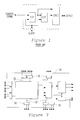
- Figure 1 is a schematic circuit diagram of a prior art glitch suppression circuit.
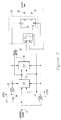
- Figure 2 is a schematic circuit diagram of the selectively bypassable glitch suppression circuit.
- Figure 3 is a functional block diagram of the bypassable glitch suppression circuit of the present invention integrated into a semiconductor chip.
- Figure 1 shows the prior art glitch suppression circuits which typically contain two bistable devices or flip-flops which sample and store the state of a control signal at two different clock intervals.
- a logic circuit provides an output signal to the operating circuit.
- Figure 2 shows a glitch suppression circuit of the present invention which includes an input terminal 10 which receives a control signal and is connected to an input terminal of a first bistable device 12 which is sampled a time T1 by the application of a clock signal from an input terminal 14.
- the bistable device 12 When toggled by the clock signal at time T2, the bistable device 12 provides an output signal which reflects the state of the control signal at time T1. This signal is applied to an input terminal of a second bistable device 16. At time T3, the clock signal causes the output state of the control signal at time T2 to be reflected as the output signal of the bistable device 12 and the output signal from the bistable device 16 to reflect the state of the control signal at time T1.
- a logic circuit responsive to the output signals from the two flip-flops provides the output signal of the glitch suppressor circuit.
- the glitch suppressor circuit provides an output signal only when the state of the control signal has remained unchanged for two successive clock cycles.
- Figure 2 shows the output signals from the bistable devices 12 and 16 are applied to the two input terminals of an Exclusive OR (“XOR") gate 18 which provides a signal to the "Clear" input terminal CL of a third flip-flop 20.
- XOR Exclusive OR
- the third flip-flop 20 is connected to function as a multiplexer for (a) the negative output signal from the bistable device 16 and (b) the output signal from the negative Q terminal of the flip-flop (through an inverter 26), and to treat the multiplexed signal as the input signal to terminal D of the flipflop 20.
- the output signal from the OR gate 22 is applied to the CL input terminal and the output signal from the OR gate 24 is applied to the "Preset" input terminal PR of the flip-flop 20. Note in Figure 2 that the terminals CL and PR have been reversed for convenience in drafting.
- the output signal from the positive Q output terminal is applied through an inverter 28 as the output signal of the glitch suppressor circuit.
- the glitch suppressor circuit of the present invention provides an output signal only when the state of the control signal has remained unchanged for two successive clock cycles.
- the circuit of the present invention provides for a selective bypass.
- Figure 2 shows a reset signal may selectively be applied by way of an input terminal 19 to one input terminal of two, two input terminal, OR gates 22 and 24.
- the control signal is applied to the other input terminal of the two OR gates 22 and 24, through an inverter 26 in the case of the OR gate 22.
- OR gate 22 provides an output signal in response to either a binary low control signal or a binary high reset signal
- OR gate 24 provides an output signal in response to either a binary high control signal or a binary high reset signal.
- an output signal from one of the two OR gates 22 and 24 will be provided for each transition of the control signal as well as a result of the application of a reset signal to the input terminal 19.
- the output signals from the OR gates 22 and 24 are applied to complementary reset terminals (i.e., CL and PR) of both of the bistable devices 12 and 16 and the flip-flop 20 so that all three will be reset.
- the glitch suppressor circuit thus becomes transparent to the control signal when a reset signal is present on the input terminal 19, and that the control signal as sampled during successive clock cycles will be propagated therethrough without the requirement that the state of the control signal remain the same for two clock cycles.
- the number of bistable devices may be increased for any given clock signal to enlarge the time period over which the state of the control signal must remain constant to be recognized as such.
- bistable devices and gates referenced herein may be any suitable conventional circuits capable of performing the functions indicated.
- other functionally equivalent circuits may be employed. Even where the same circuit elements are used, the connections may be varied, with the addition or deletion of inverters, to balance the use of positive and negative gong output signals, etc.
- the present invention permits the integration of the glitch suppressor circuit 30 of the present invention into each control line 32 of an integrated circuit 34 without regard for such considerations, with knowledge that the decision as to whether and when to include may be later resolved by the selective application of a simple reset signal.
- the glitch suppressor circuits By designing the glitch suppressor circuits into each control line 32 of the IC 34, the cost of the glitch suppressor circuit is significantly reduced.
- each of the glitch suppressor circuits i.e., one each for the control signal, clock and reset signal.
- the clock signal may be provided from one or more sources internal of the IC 34 and the necessity for the third external connection thus obviated.
- the glitch suppressor circuit of the present invention may be used as a filter, to reduce the noise sensitivity of a circuit, to debounce switch contacts thus permitting direct connection to the IC, and to suppress the effects of sampling during transition of the control signal due to a lock of synchronism between the clock and control signals.
- the integration of the glitch suppression circuit into the IC subjects it to the same process parameters during manufacturing and subjects it to the same temperature conditions during operation.
- the glitch suppression circuit imposes no constraints on the IC.
- a resettable glitch suppression circuit integrated into each input control line of a semiconductor chip to provide flexibility for each control line as to whether or not, and if so when, the glitch suppression circuit is operable.
Landscapes
- Physics & Mathematics (AREA)
- Nonlinear Science (AREA)
- Manipulation Of Pulses (AREA)
- Semiconductor Integrated Circuits (AREA)
- Electronic Switches (AREA)
- Credit Cards Or The Like (AREA)
Applications Claiming Priority (2)
| Application Number | Priority Date | Filing Date | Title |
|---|---|---|---|
| US83517 | 1993-06-30 | ||
| US08/083,517 US5386159A (en) | 1993-06-30 | 1993-06-30 | Glitch suppressor circuit and method |
Publications (2)
| Publication Number | Publication Date |
|---|---|
| EP0632590A1 EP0632590A1 (en) | 1995-01-04 |
| EP0632590B1 true EP0632590B1 (en) | 1999-03-24 |
Family
ID=22178842
Family Applications (1)
| Application Number | Title | Priority Date | Filing Date |
|---|---|---|---|
| EP94304699A Expired - Lifetime EP0632590B1 (en) | 1993-06-30 | 1994-06-28 | Glitch suppressor circuit and method |
Country Status (8)
| Country | Link |
|---|---|
| US (1) | US5386159A (OSRAM) |
| EP (1) | EP0632590B1 (OSRAM) |
| JP (1) | JPH0758609A (OSRAM) |
| CN (1) | CN1091552C (OSRAM) |
| CA (1) | CA2126615C (OSRAM) |
| DE (1) | DE69417297T2 (OSRAM) |
| MY (1) | MY111002A (OSRAM) |
| NO (1) | NO942407L (OSRAM) |
Families Citing this family (16)
| Publication number | Priority date | Publication date | Assignee | Title |
|---|---|---|---|---|
| DE19812420A1 (de) * | 1998-03-20 | 1999-09-23 | Moeller Gmbh | Umstellbare Entprellung |
| CN1077453C (zh) * | 1998-12-25 | 2002-01-09 | 华南理工大学 | 碱木素羟甲基化多相反应催化剂及其制备方法 |
| KR100343139B1 (ko) * | 1999-11-22 | 2002-07-05 | 윤종용 | 데이터 동기화 회로 |
| DE19960785A1 (de) * | 1999-12-16 | 2001-06-21 | Thomson Brandt Gmbh | Eingangsfilterstufe für einen Datenstrom und Verfahren zum Filtern eines Datenstroms |
| US6914951B2 (en) * | 2001-07-24 | 2005-07-05 | Hewlett-Packard Development Company, L.P. | Method and apparatus for a digital logic input signal noise filter |
| US20030163627A1 (en) * | 2002-02-28 | 2003-08-28 | Deng Brian Tse | Enhanced universal serial bus (USB) bus monitor controller |
| US6891415B2 (en) * | 2002-06-11 | 2005-05-10 | Micron Technology, Inc. | Method and apparatus for enabling a timing synchronization circuit |
| JP2004139438A (ja) * | 2002-10-18 | 2004-05-13 | Matsushita Electric Ind Co Ltd | 押下判定システム |
| US7426960B2 (en) * | 2005-05-03 | 2008-09-23 | Luca Technologies, Inc. | Biogenic fuel gas generation in geologic hydrocarbon deposits |
| CN100419623C (zh) * | 2005-08-24 | 2008-09-17 | 纬创资通股份有限公司 | 抗杂讯干扰的系统及其方法 |
| US7667500B1 (en) * | 2006-11-14 | 2010-02-23 | Xilinx, Inc. | Glitch-suppressor circuits and methods |
| ITTO20090334A1 (it) * | 2009-04-28 | 2010-10-29 | St Microelectronics Srl | Dispositivo e metodo di protezione da disturbi per un segnale digitale |
| US10277213B1 (en) * | 2017-10-26 | 2019-04-30 | Nxp Usa, Inc. | Glitch detection in input/output bus |
| CN108365841A (zh) * | 2018-01-11 | 2018-08-03 | 北京国睿中数科技股份有限公司 | 门控时钟的控制系统和控制方法 |
| US11177799B2 (en) | 2019-10-18 | 2021-11-16 | Stmicroelectronics International N.V. | Debounce circuit with noise immunity and glitch event tracking |
| CN112688670B (zh) * | 2019-10-18 | 2024-12-13 | 意法半导体国际有限公司 | 具有抗噪性和毛刺事件跟踪的去抖动电路 |
Family Cites Families (9)
| Publication number | Priority date | Publication date | Assignee | Title |
|---|---|---|---|---|
| US3886543A (en) * | 1973-11-29 | 1975-05-27 | Teletype Corp | Debounce logic for keyboard |
| US4353032A (en) * | 1980-06-02 | 1982-10-05 | Tektronix, Inc. | Glitch detector |
| US4427948A (en) * | 1981-12-21 | 1984-01-24 | Gte Automatic Electric Labs Inc. | Pulse toggle monitor circuit |
| US4525635A (en) * | 1982-12-15 | 1985-06-25 | Rca Corporation | Transient signal suppression circuit |
| JPS62151053A (ja) * | 1985-12-25 | 1987-07-06 | Iwatsu Electric Co Ltd | ノイズ除去回路 |
| DE3913395A1 (de) * | 1989-04-24 | 1990-10-25 | Grundig Emv | Digitale filterlogik |
| JPH02283120A (ja) * | 1989-04-25 | 1990-11-20 | Toshiba Corp | 雑音除去装置 |
| US5001374A (en) * | 1989-09-08 | 1991-03-19 | Amp Incorporated | Digital filter for removing short duration noise |
| IT1243301B (it) * | 1990-05-25 | 1994-05-26 | Sgs Thomson Microelectronics | Circuito di filtraggio di un segnale logico affetto da spikes di commutazione |
-
1993
- 1993-06-30 US US08/083,517 patent/US5386159A/en not_active Expired - Lifetime
-
1994
- 1994-06-22 MY MYPI94001616A patent/MY111002A/en unknown
- 1994-06-23 CA CA002126615A patent/CA2126615C/en not_active Expired - Fee Related
- 1994-06-24 NO NO942407A patent/NO942407L/no not_active Application Discontinuation
- 1994-06-28 EP EP94304699A patent/EP0632590B1/en not_active Expired - Lifetime
- 1994-06-28 DE DE69417297T patent/DE69417297T2/de not_active Expired - Fee Related
- 1994-06-28 JP JP6146769A patent/JPH0758609A/ja active Pending
- 1994-06-29 CN CN94107836A patent/CN1091552C/zh not_active Expired - Fee Related
Also Published As
| Publication number | Publication date |
|---|---|
| US5386159A (en) | 1995-01-31 |
| JPH0758609A (ja) | 1995-03-03 |
| CN1139315A (zh) | 1997-01-01 |
| EP0632590A1 (en) | 1995-01-04 |
| NO942407L (no) | 1995-01-02 |
| NO942407D0 (OSRAM) | 1994-06-24 |
| CN1091552C (zh) | 2002-09-25 |
| CA2126615C (en) | 2003-11-04 |
| MY111002A (en) | 1999-07-31 |
| DE69417297T2 (de) | 1999-11-04 |
| CA2126615A1 (en) | 1994-12-31 |
| DE69417297D1 (de) | 1999-04-29 |
Similar Documents
| Publication | Publication Date | Title |
|---|---|---|
| EP0632590B1 (en) | Glitch suppressor circuit and method | |
| US6163166A (en) | Programmable logic device with selectable schmitt-triggered and threshold-triggered buffers | |
| US4929850A (en) | Metastable resistant flip-flop | |
| US5489865A (en) | Circuit for filtering asynchronous metastability of cross-coupled logic gates | |
| JP3057814B2 (ja) | 半導体集積回路 | |
| US5319646A (en) | Boundary-scan output cell with non-critical enable path | |
| US5148052A (en) | Recirculating transparent latch employing a multiplexing circuit | |
| US5625309A (en) | Bistable sequential logic network that is sensitive to the edges of input signals | |
| US5388225A (en) | Time-domain boundary bridge method and apparatus for asynchronous sequential machines | |
| US6348828B1 (en) | Clock enable circuit for use in a high speed reprogrammable delay line incorporating glitchless enable/disable functionality | |
| CN114189323B (zh) | 通讯时钟复位信号处理电路及方法 | |
| US20070240094A1 (en) | Partially gated mux-latch keeper | |
| JP2644111B2 (ja) | 入出力回路 | |
| JP2003163583A (ja) | 非同期型ノイズフィルタ回路 | |
| JP3168089B2 (ja) | チャタリング除去回路 | |
| JP2504190B2 (ja) | チャタリング防止回路 | |
| JPH04101535A (ja) | インタフェース回路 | |
| JPH0529892A (ja) | 論理回路 | |
| KR0177756B1 (ko) | 노이즈제거회로 | |
| KR0172414B1 (ko) | 글리치 제거 회로 | |
| SU1218455A1 (ru) | Формирователь импульсов | |
| SU1193608A1 (ru) | Устройство контрол больших интегральных схем | |
| SU1205274A1 (ru) | Формирователь одиночных импульсов | |
| JPH0713655A (ja) | 半導体集積回路 | |
| JPS5922975B2 (ja) | 信号優先順位決定回路 |
Legal Events
| Date | Code | Title | Description |
|---|---|---|---|
| PUAI | Public reference made under article 153(3) epc to a published international application that has entered the european phase |
Free format text: ORIGINAL CODE: 0009012 |
|
| AK | Designated contracting states |
Kind code of ref document: A1 Designated state(s): DE FR GB IT SE |
|
| 17P | Request for examination filed |
Effective date: 19950628 |
|
| 17Q | First examination report despatched |
Effective date: 19960809 |
|
| GRAG | Despatch of communication of intention to grant |
Free format text: ORIGINAL CODE: EPIDOS AGRA |
|
| GRAG | Despatch of communication of intention to grant |
Free format text: ORIGINAL CODE: EPIDOS AGRA |
|
| GRAH | Despatch of communication of intention to grant a patent |
Free format text: ORIGINAL CODE: EPIDOS IGRA |
|
| GRAH | Despatch of communication of intention to grant a patent |
Free format text: ORIGINAL CODE: EPIDOS IGRA |
|
| GRAA | (expected) grant |
Free format text: ORIGINAL CODE: 0009210 |
|
| AK | Designated contracting states |
Kind code of ref document: B1 Designated state(s): DE FR GB IT SE |
|
| REF | Corresponds to: |
Ref document number: 69417297 Country of ref document: DE Date of ref document: 19990429 |
|
| ET | Fr: translation filed | ||
| PLBE | No opposition filed within time limit |
Free format text: ORIGINAL CODE: 0009261 |
|
| STAA | Information on the status of an ep patent application or granted ep patent |
Free format text: STATUS: NO OPPOSITION FILED WITHIN TIME LIMIT |
|
| 26N | No opposition filed | ||
| REG | Reference to a national code |
Ref country code: GB Ref legal event code: IF02 |
|
| PGFP | Annual fee paid to national office [announced via postgrant information from national office to epo] |
Ref country code: FR Payment date: 20050617 Year of fee payment: 12 |
|
| PGFP | Annual fee paid to national office [announced via postgrant information from national office to epo] |
Ref country code: SE Payment date: 20050621 Year of fee payment: 12 |
|
| PGFP | Annual fee paid to national office [announced via postgrant information from national office to epo] |
Ref country code: GB Payment date: 20050622 Year of fee payment: 12 |
|
| PGFP | Annual fee paid to national office [announced via postgrant information from national office to epo] |
Ref country code: DE Payment date: 20050801 Year of fee payment: 12 |
|
| PG25 | Lapsed in a contracting state [announced via postgrant information from national office to epo] |
Ref country code: GB Free format text: LAPSE BECAUSE OF NON-PAYMENT OF DUE FEES Effective date: 20060628 |
|
| PG25 | Lapsed in a contracting state [announced via postgrant information from national office to epo] |
Ref country code: SE Free format text: LAPSE BECAUSE OF NON-PAYMENT OF DUE FEES Effective date: 20060629 |
|
| PGFP | Annual fee paid to national office [announced via postgrant information from national office to epo] |
Ref country code: IT Payment date: 20060630 Year of fee payment: 13 |
|
| PG25 | Lapsed in a contracting state [announced via postgrant information from national office to epo] |
Ref country code: DE Free format text: LAPSE BECAUSE OF NON-PAYMENT OF DUE FEES Effective date: 20070103 |
|
| EUG | Se: european patent has lapsed | ||
| GBPC | Gb: european patent ceased through non-payment of renewal fee |
Effective date: 20060628 |
|
| REG | Reference to a national code |
Ref country code: FR Ref legal event code: ST Effective date: 20070228 |
|
| PG25 | Lapsed in a contracting state [announced via postgrant information from national office to epo] |
Ref country code: FR Free format text: LAPSE BECAUSE OF NON-PAYMENT OF DUE FEES Effective date: 20060630 |
|
| PG25 | Lapsed in a contracting state [announced via postgrant information from national office to epo] |
Ref country code: IT Free format text: LAPSE BECAUSE OF NON-PAYMENT OF DUE FEES Effective date: 20070628 |