EP0631446B1 - Signal processor for video tape recorder - Google Patents
Signal processor for video tape recorder Download PDFInfo
- Publication number
- EP0631446B1 EP0631446B1 EP94304485A EP94304485A EP0631446B1 EP 0631446 B1 EP0631446 B1 EP 0631446B1 EP 94304485 A EP94304485 A EP 94304485A EP 94304485 A EP94304485 A EP 94304485A EP 0631446 B1 EP0631446 B1 EP 0631446B1
- Authority
- EP
- European Patent Office
- Prior art keywords
- frequency
- signal
- signals
- color
- carrier
- Prior art date
- Legal status (The legal status is an assumption and is not a legal conclusion. Google has not performed a legal analysis and makes no representation as to the accuracy of the status listed.)
- Expired - Lifetime
Links
- 230000003111 delayed effect Effects 0.000 claims description 31
- 238000006243 chemical reaction Methods 0.000 claims description 22
- 239000000969 carrier Substances 0.000 claims description 20
- 230000000694 effects Effects 0.000 claims description 12
- 238000010586 diagram Methods 0.000 description 22
- 230000004044 response Effects 0.000 description 15
- 239000006185 dispersion Substances 0.000 description 11
- 238000000034 method Methods 0.000 description 11
- 230000003534 oscillatory effect Effects 0.000 description 9
- 238000010276 construction Methods 0.000 description 8
- 230000001360 synchronised effect Effects 0.000 description 8
- 230000010363 phase shift Effects 0.000 description 7
- 238000007792 addition Methods 0.000 description 5
- 239000011521 glass Substances 0.000 description 5
- 239000004065 semiconductor Substances 0.000 description 4
- 239000010453 quartz Substances 0.000 description 3
- VYPSYNLAJGMNEJ-UHFFFAOYSA-N silicon dioxide Inorganic materials O=[Si]=O VYPSYNLAJGMNEJ-UHFFFAOYSA-N 0.000 description 3
- 230000002238 attenuated effect Effects 0.000 description 2
- 229910021419 crystalline silicon Inorganic materials 0.000 description 1
- 230000002950 deficient Effects 0.000 description 1
- 239000000284 extract Substances 0.000 description 1
- 230000006870 function Effects 0.000 description 1
- 238000011835 investigation Methods 0.000 description 1
- 238000004519 manufacturing process Methods 0.000 description 1
- 238000004806 packaging method and process Methods 0.000 description 1
- 230000000630 rising effect Effects 0.000 description 1
- 239000007787 solid Substances 0.000 description 1
- 239000000758 substrate Substances 0.000 description 1
Images


Classifications
-
- H—ELECTRICITY
- H04—ELECTRIC COMMUNICATION TECHNIQUE
- H04N—PICTORIAL COMMUNICATION, e.g. TELEVISION
- H04N9/00—Details of colour television systems
- H04N9/79—Processing of colour television signals in connection with recording
- H04N9/80—Transformation of the television signal for recording, e.g. modulation, frequency changing; Inverse transformation for playback
- H04N9/82—Transformation of the television signal for recording, e.g. modulation, frequency changing; Inverse transformation for playback the individual colour picture signal components being recorded simultaneously only
- H04N9/83—Transformation of the television signal for recording, e.g. modulation, frequency changing; Inverse transformation for playback the individual colour picture signal components being recorded simultaneously only the recorded chrominance signal occupying a frequency band under the frequency band of the recorded brightness signal
-
- G—PHYSICS
- G11—INFORMATION STORAGE
- G11B—INFORMATION STORAGE BASED ON RELATIVE MOVEMENT BETWEEN RECORD CARRIER AND TRANSDUCER
- G11B20/00—Signal processing not specific to the method of recording or reproducing; Circuits therefor
-
- H—ELECTRICITY
- H04—ELECTRIC COMMUNICATION TECHNIQUE
- H04N—PICTORIAL COMMUNICATION, e.g. TELEVISION
- H04N9/00—Details of colour television systems
- H04N9/79—Processing of colour television signals in connection with recording
- H04N9/793—Processing of colour television signals in connection with recording for controlling the level of the chrominance signal, e.g. by means of automatic chroma control circuits
-
- H—ELECTRICITY
- H04—ELECTRIC COMMUNICATION TECHNIQUE
- H04N—PICTORIAL COMMUNICATION, e.g. TELEVISION
- H04N9/00—Details of colour television systems
- H04N9/79—Processing of colour television signals in connection with recording
- H04N9/80—Transformation of the television signal for recording, e.g. modulation, frequency changing; Inverse transformation for playback
- H04N9/82—Transformation of the television signal for recording, e.g. modulation, frequency changing; Inverse transformation for playback the individual colour picture signal components being recorded simultaneously only
- H04N9/83—Transformation of the television signal for recording, e.g. modulation, frequency changing; Inverse transformation for playback the individual colour picture signal components being recorded simultaneously only the recorded chrominance signal occupying a frequency band under the frequency band of the recorded brightness signal
- H04N9/84—Transformation of the television signal for recording, e.g. modulation, frequency changing; Inverse transformation for playback the individual colour picture signal components being recorded simultaneously only the recorded chrominance signal occupying a frequency band under the frequency band of the recorded brightness signal the recorded signal showing a feature, which is different in adjacent track parts, e.g. different phase or frequency
Definitions
- the present invention relates to a signal processor for a VTR (which is abbreviated from Video Tape Recorder as in the following) and, more particularly, to a technique which is effective if applied to a frequency converter for converting the reproduced video signals of a color under system such as the VHS, S-VHS or 8 mm video system into standard color signals.
- VTR Video Tape Recorder
- color video signals are recorded by the color under system.
- the luminance signals are frequency-modulated, and the color signals are frequency-converted to a lower frequency band than that of the frequency-modulated luminance signals and are recorded on the inclined track of a magnetic tape by a rotary video head.
- the VTR of recent years uses the guard bandless system for a higher density and is essentially required to clear a noise (as will be called the "crosstalk component") caused by a crosstalk.
- the clearance of this crosstalk component is effected by giving an azimuth angle to the video head, and this azimuth angle is effective highly for high-frequency signals but lowly for low-frequency signals. In other words, the clearance of the crosstalk component is little effective for the color signals, and the phase shift system (i.e., the PS system) or the phase invert system (i.e., the PI system) is adopted for the effect.
- a method of clearing the crosstalk component in the color under system will be described by using the NTSC format of the VHS system.
- the video recording track is recorded by alternating two tracks, i.e., Channel 1 and Channel 2.
- the standard color signals are recorded by converting their sub-carrier frequency of 3.579545 MHz into 40 f H , i.e., about 629 KHz.
- the phases are advanced for one horizontal period (1 H) by 90 degrees in Channel 1 and delayed by 90 degrees in Channel 2.
- the reproduced color under signals delayed by one horizontal period (1 H) can be added to clear the crosstalk components by using a delay element of one horizontal period (1 H) and by using the reproduced color under signals before delayed and the delay element.
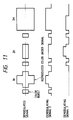
- Fig. 12 and 13 The frequency conversion technique we have investigated before our invention is shown in Fig. 12, Fig. 13 and Fig. 14.
- the crosstalk component is cleared by converting the reproduced color under signals into the standard color signals of 3.579545 MHz with a main converter and then by delaying the standard color signals by one horizontal period (1 H) with a glass delay line or a CCD (i.e., Charge Coupled Device as in the following).
- the phase adjustment is omitted by delaying the low-pass reproduced color under signals by one horizontal period (1 H) or two horizontal periods (2 H) in the low frequency with the CCD and by adding it to or subtracting it from the reproduced color under signals before delayed.
- the aforementioned frequency conversion technique is exemplified by Japanese Patent Laid-Open No. 257394 /1988 or 51489/1990.
- the aforementioned method using the glass delay line is defective in that the glass delay line is a part relatively large to be packaged and expensive in price.
- the method using the CCD has to operate at a clock three or four times as high as 3.579545 MHz of the sub-carriers, and a phase adjustment is required for adjusting the total delay of the CCD and a low-pass filter or a band-pass filter necessary downstream of the CCD accurately to one horizontal period (1 H).
- This phase adjustment has to be several degrees or less with respect to the accuracy of the sub-carrier frequency of 3.579545 MHz.
- the method of Fig. 14 can be practised by an inexpensive CCD having a low clock frequency.
- EP 0476922A and US 4991026 disclose video signal processing using four signals with frequency related to a carrier frequency and a mutual phase difference of 90°.
- An aim of the present invention is to permit a signal processor a signal processor for a VTR to be produced, which can convert a reproduced frequency while clearing a crosstalk component by a simple construction.
- Another preferred aim of the present invention is to provide a VTR signal processor which can have a simple construction and automatically eliminate the amplitude level difference (or gain dispersion) between the reproduced color under signal produced due to the element dispersion of the aforementioned delay circuit or the like and the delayed reproduced color under signal.
- the present invention provides a signal processor for a video tape recorder comprising:
- the clock frequency of the delay circuit of the CCD or the like for delaying the reproduced color under signals can be lowered and simplified, and it is possible to automatically eliminate the amplitude level difference (or gain dispersion) between the reproduced color under signal produced due to the element dispersion of the aforementioned delay circuit or the like and the delayed reproduced color under signal.
- the output signals of two frequency converters 3 and 4 can have their phases adjusted by feeding the four signals selectively to the frequency converters 3 and 4 in response to the reproduced color under signals inputted, so that the crosstalk component can be eliminated by making an addition or subtraction by an arithmetic circuit.
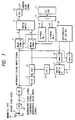
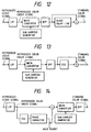
- Fig. 1 is a block diagram showing one embodiment of a frequency conversion unit to be incorporated into a VTR signal processor according to the present invention.
- the circuit block of Fig. 1 is formed together with other circuit blocks composing the VTR signal processor over a single semiconductor substrate of single-crystalline silicon by the well-known technique of manufacturing a semiconductor integrated circuit.
- reference numeral 22 designates a preamplifier (PA) for amplifying the signals which are read out of a magnetic tape 20 by a rotary video head 21.
- the signals thus amplified by the aforementioned preamplifier are fed as reproduced video signals through a terminal T1 to a low-pass filter (LPF) 1.
- This low-pass filter (LPF) 1 extracts a color signal from the reproduced video signals outputted from the aforementioned preamplifier (PA) 22.
- Numeral 2 designates a delay signal for one horizontal period (1 H) or two horizontal periods (2 H).
- This delay circuit 2 may be composed of not only a CCD but also an input portion for analog/digital conversion, a shift register for the delay, and a digital/analog converter for returning the shifted digital signal to an analog signal.
- Numeral 3 designates a first frequency converter for converting the reproduced color under signal before delayed into the frequency of a standard color signal.
- Numeral 4 designates a second frequency converter, i.e., the so-called "main converter” for converting the reproduced color under signal delayed by the aforementioned delay circuit 2 into the frequency of a standard color signal.
- Numeral 5 designates an arithmetic circuit (for Arithmetic 1) for clearing a crosstalk component from the output signals of the frequency converters 3 and 4.
- the aforementioned reproduced video signal is fed to the low-pass filter 1 for separating it from a luminance signal.
- the low-pass filter 1 outputs the reproduced color under signal.
- This reproduced color under signal is delayed on one hand by one horizontal period (1 H) and is guided through a gain controller (i.e., GCA) 6 to the second frequency converter (Main Conv2) 4.
- GCA gain controller
- Mainn Conv2 the second frequency converter
- the color signals thus having their frequencies converted by the aforementioned first and second frequency converters 3 and 4 are fed to the arithmetic circuit 5 for clearing the crosstalk component.
- a band-pass filter i.e., BPF 16
- the unnecessary frequency components produced by the first and second frequency converters 3 and 4 can be cleared to produce clear standard color signals.
- 2fL VCO an oscillator
- the reproduced color under signal inputted to the first frequency converter 3 and the reproduced color under signal inputted to the second frequency converter 4 and delayed by one horizontal period (1 H) are inputted to demodulators (Demol and Demo2) 7 and 8, respectively, so that their amplitude levels may be equalized.
- demodulators 7 and 8 demodulated signals of base band are produced by using the sub-carrier which has its frequency synchronized with the burst signal of the reproduced color under signal fed from a sub-carrier generator 15.
- the demodulated signals are fed through an arithmetic circuit (Arithmetic 2) 9 for establishing the amplitude difference of the demodulated base bands and are converted into DC voltages by a low-pass filter (LPF2) 10, and the reproduced color under signal inputted to the first frequency converter 3 and the reproduced color under signal inputted to the second frequency converter 4 and delayed by one horizontal period (1 H) have their amplitude levels equalized by controlling the aforementioned gain controller (GCA) 6.
- Arithmetic 2 arithmetic circuit for establishing the amplitude difference of the demodulated base bands and are converted into DC voltages by a low-pass filter (LPF2) 10, and the reproduced color under signal inputted to the first frequency converter 3 and the reproduced color under signal inputted to the second frequency converter 4 and delayed by one horizontal period (1 H) have their amplitude levels equalized by controlling the aforementioned gain controller (GCA) 6.
- Arithmetic 2 arithmetic circuit for establishing the amplitude difference of the demodulated base bands and are converted
- the oscillator 11 oscillates at a frequency of 2n x fL (fL: the sub-carrier frequency) for producing a sub-carrier for frequency conversion, and the frequency divider 12 divides the frequency of the frequency of the oscillator 11 into the frequency of the sub-carriers, although not especially limited thereto, and produces of sub-carriers of four phases of 0, 90, 180 and 270 degrees.
- the aforementioned 4-phase sub-carriers are individually fed to the aforementioned 4-phase switches 13 and 14.
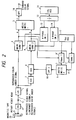
- Fig. 2 is a block diagram showing another embodiment of the frequency conversion unit to be incorporated into a VTR signal processor according to the present invention.
- the color signal having its frequency converted by the first frequency converter 3 and the color signal having its frequency converted by the second frequency converter 4 are inputted to demodulators (Demol and Demo2) 7' and 8' so that their amplitude levels may be equalized.
- demodulators 7' and 8' perform the demodulations to produce color signals with the frequency-converted color signals and the color carrier (fsc) produced by the oscillator 17.
- Figs. 3A and 3B are schematic diagrams showing one embodiment of the arithmetic circuit for clearing the aforementioned crosstalk component.
- Figs. 3A and 3B shows the case, in which A signal and B signal are in phase if the aforementioned color signal outputted from the aforementioned first frequency converter 3 is called the A signal whereas the aforementioned color signal outputted from the aforementioned second second frequency converter 4 is called the B signal.
- the crosstalk component is cleared from the A signal by subtracting the B signal from the A signal to extract a double crosstalk component, by attenuating it by -6 dB, i.e., by halving its level to return it to the crosstalk component, and by subtracting it from the A signal.
- Figs. 4A and 4B are schematic diagrams showing another embodiment of the arithmetic circuit for clearing the aforementioned crosstalk component.
- Figs. 4A and 4B show the case, in which A signal and B signal are in opposite phases if the aforementioned color signal outputted from the aforementioned first frequency converter 3 is called the A signal whereas the aforementioned color signal outputted from the aforementioned second second frequency converter 4 is called the B signal.
- the crosstalk component is cleared from the A signal by adding the A signal and the B signal to extract a double crosstalk component, by attenuating it by -6 dB, i.e., by halving its level to return it to the crosstalk component, and by subtracting it from the A signal.
- the crosstalk components in phase are offset by subtracting the B signal from the A signal. By this subtraction, the signal component in opposite phase is doubled so that the initial signal level is restored even by the attenuation of -6 dB.
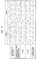
- Fig. 9 is a phase shift diagram enumerates reproduced color under signals in the NTSC format of the VHS system, that is, the color signals (i.e., the A signal and the B signal) having their frequencies converted by the aforementioned two frequency converters 3 and 4 and the aforementioned standard color signals.
- Fig. 9 (a) enumerates the phase of the reproduced color under signal of Channel 1; (b) the phase of the reproduced color under signal of Channel 2; (c) the phase of the reproduced color under signal of (a) of Channel 1 after delay of one horizontal period (1 H); and (d) the phase of the reproduced color under signal of (b) of Channel 2 after delay of one horizontal period (1 H).
- Solid lines indicate signal components, and broken lines indicate crosstalk components.
- These sub-carriers of four phases are fed to the first and second frequency converters by the switches 13 and 14.
- the phases of the sub-carriers fed at this time to the switches 13 and 14 are set to return the phase shifts at the recording time. Specifically, the phase is advanced in Channel 1 by 90 degrees for each horizontal period (1 H) and is delayed in Channel 2 by 90 degrees for each horizontal period (1 H).
- the phase of the sub-carrier of the second frequency converter 4 is delayed by 90 degrees in Channel 1 and advanced by 90 degrees in Channel 2 from the sub-carrier phase of the first frequency converter 3.
- the phases of 3.579545 MHz converted by those first and second frequency converters 3 and 4 are enumerated in (e), (f), (g) and (h).
- the phase (i) is obtained in Channel 1 by adding the phases (e) and (g) by the adder of the arithmetic circuit 5, and the phase (j) is obtained in Channel 2 by adding the phases (f) and (h).
- the crosstalk components as indicated by broken lines, can be cleared to produce the standard color signals having their frequencies converted. Incidentally, the mere addition would double the signal level, and the added output has to be attenuated by -6 dB, as shown in Figs. 3A and 3B.
- the crosstalk components can also be cleared, as described above, by using a subtracter.
- the frequency conversion may be started from any of the four phases, as shown at (a).
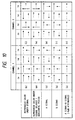
- Fig. 10 is a phase shift diagram enumerates reproduced color under signals in the PAL format of the VHS system, that is, the color signals (i.e., the A signal and the B signal) having their frequencies converted by the aforementioned two frequency converters 3 and 4 and the aforementioned standard color signals.
- solid lines indicate signal components, and broken lines indicate crosstalk components.
- (k) enumerates the phase of the reproduced color under signal of Channel 1;
- the phase of the sub-carrier of the second frequency converter 4 is set in Channel 1 to the same phase as that of the frequency converter 3 and is advanced by 180 degrees in Channel 2 from the same.
- the phases of 4.433618 MHz converted by those first and second frequency converters 3 and 4 are enumerated in (o), (p), (q) and (r).
- the phase (s) is obtained in Channel 1 by adding the output signals (o) and (q)
- the phase (t) is obtained in Channel 2 by adding the output signals (p) and (r).
- the crosstalk components can be eliminated to produce the frequency-converted standard color signals.
- the frequency conversion may be started from any of the four phases, as indicated at (k). This discussion likewise applies to Channel 2.
- the carrier phase of the frequency conversion may be set to clear the crosstalk component. If the sub-carrier of the second frequency converter 4 is different by 180 degrees from the a-forementioned value, the crosstalk component can be cleared by exemplifying the arithmetic circuit 5 by a subtracter to produce the standard color signal having a converted frequency. In short, the crosstalk components can be cleared by the aforementioned arithmetic operation shown in Figs. 4A and 4B.
- the present invention can be applied all the color under recording/playing systems by subjecting the sub-carriers of the first and second frequency converters 3 and 4 to different phase controls.
- the gain controller 6 and the circuit group (including the demodulators 7 and 8, the arithmetic circuit 9, the low-pass filter 10 and the sub-carrier generator 15) for producing control signals for the former are those for correcting the gain dispersion of the delay circuit 2 automatically.
- the demodulators 7 and 8 demodulate the reproduced color under signals before and after the delay, and have the same demodulation gains as those of multiplication of the sub-carriers which have their frequencies synchronized with the reproduced color under signals and which are fed from the aforementioned sub-carrier generator 15.
- a demodulated signal as indicated at E in Fig.
- the demodulated signal can be produced in the NTSC format of the VHS system, for example, if the phase of the sub-carrier is advanced in Channel 1 by 90 degrees for each horizontal period (1 H) and is delayed in Channel 2 by 90 degrees for each horizontal period (1 H).
- the demodulated signal is produced, as indicated at F, if the phase of the sub-carrier of the demodulator 8 is delayed in Channel 1 by 90 degrees from the sub-carrier phase of the demodulator 7.
- the difference between the demodulated signals E and F resides in that the signal F is delayed by one horizontal period (1 H) from the signal E and that the amplitude level depends upon the amplitude level of the demodulated signal inputted to the demodulator.
- demodulated signals E and F are inputted to the arithmetic circuit (e.g., a subtracter) 9 so that its difference signal is extracted.
- This difference signal is inputted to the low-pass filter 10.
- the aforementioned differential component is detected as the DC signal.
- the level of this DC signal is proportional for a long time period, e.g., one field to the amplitude level difference of the demodulated signals inputted to the individual demodulators.
- the demodulated signals inputted to the two demodulators 7 and 8 can have their amplitude levels equalized by feeding back that DC signal to the gain controller 6.
- the phases of the sub-carriers may be set to equalize the amplitude levels of the demodulated signals inputted to the two demodulators 7 and 8. If the sub-carrier of the demodulator 8 is different by 180 degrees from the aforementioned value, an identical result can be obtained by exemplifying the arithmetic circuit 9 by an adder. In short, the present invention can be applied to all the color under recording/ playing systems by controlling the phases of the sub-carriers of the two demodulators 7 and 8.
- the gain controller 6 and the circuit group (including the demodulators 7' and 8', the arithmetic circuit 9, the low-pass filter 10 and the oscillator 17) for producing the control signals for the former are circuits for automatically correcting the gain dispersion in the delay circuit 2 and the frequency converter.
- the demodulators 7' and 8' demodulate the signals of the reproduced color under signals before and after the delay into the standard color signals and the frequency-converted signals into the demodulated signals, and have equal demodulation gains with the carriers which have their frequencies and phases synchronized with those of the burst signals of the standard color signals.
- the demodulated signal as indicated at E in Fig. 11, is obtained as that of the demodulator 7'.
- the demodulated signal, as indicated at F, is obtained as that of the demodulator 8'.
- the signal F is delayed by one horizontal period (1 H) from the signal E and that the amplitude level depends upon the amplitude level of the demodulated signals inputted to the demodulators.
- the phases of the demodulated carriers may be set to equalize the amplitude levels of the demodulated signals inputted to the two demodulators 7' and 8'. If the sub-carrier of the demodulator 8' is different by 180 degrees from the aforementioned value, an identical result can be obtained by exemplifying the arithmetic circuit 9 by an adder. In short, the present invention can be applied to all the color under recording/playing systems by controlling the phases of the sub-carriers of the two demodulators 7' and 8'.
- a frequency converter capable of clearing the crosstalk components by the CCD or line memory having a low clock frequency can be provided in the color under type VTR without using either any large part having a large packaging area such as the glass delay line or the CCD having a high clock frequency and without adding any phase corrector to the color signal route or the sub-carrier route.
- the frequency conversion unit as shown in Fig. 1, can be constructed and automatically adjusted even with an element dispersion in the delay circuit of one horizontal periods (1H) or two horizontal periods (2H).
- Fig. 5 is a block diagram for explaining the frequency converting system premising the present invention.
- a frequency which is N times as high as that of the signal f c , is produced by the voltage-control type oscillator (as will be shortly referred to as the "VCO") and is synchronized with a horizontal synchronizing signal by a PLL (i.e., Phase Locked Loop).
- VCO voltage-control type oscillator
- PLL Phase Locked Loop
- the VCO is given a free-running frequency corresponding substantially to a frequency of 535 f H which is two times as high as that of the carrier signal f c , although not especially limited thereto.
- the output signal of that VCO has its frequency halved to produce the carrier signal f c of the aforementioned frequency 535 f H /2.
- the frequency divider used is exemplified by a through latch circuit having the ECL construction, as will be described hereinafter, to effect the aforementioned frequency division and to produce 4-phase signals having a phase difference of 90 degrees from each other.
- the following loop is provided for synchronizing that carrier signal accurately with the horizontal synchronizing signal contained in the recorded signals.
- DFF D-type flip-flop circuit
- This DFF has its data terminal D fed with a frequency corresponding to the color sub-carrier of about 3.58 MHz produced by a quartz oscillator.
- This DFF is enabled, by fetching the signal of a lower frequency of 3.58 MHz in synchronism with the rising edge of the higher frequency 4.21 MHz, as illustrated in the waveform diagram of Fig. 8, to produce a phase difference inbetween, i.e., an output signal corresponding to the frequency difference, from an output terminal Q.
- the aforementioned carrier signal having the frequency of 535 f H / 2 may be divided into 2/535 by the frequency divider. In this case, however, the frequency division of a fraction of 2/535 is required to complicate the circuit and enlarge the circuit scale.
- the frequency divider in the PLL can be drastically simplified.
- the frequency divider disposed in the aforementioned PLL performs a frequency division of 1/40 to produce a frequency signal corresponding to the horizontal synchronizing signal f H .
- This frequency-divided output signal is fed together with the horizontal synchronizing signal f H contained in the recording signal fed from a record terminal R so that they are compared in phase.
- the aforementioned horizontal synchronizing signal f H is produced through the not-shown synchronous separator.
- the detected signal corresponding to the phase difference (i.e., frequency difference) is converted into a DC signal by the low-pass filter (as will be shortly referred to as the "LPF") and is fed to the control terminal of the aforementioned VCO through the switch SW2 which is connected to the recording side REC when in the recording mode.
- the low-pass filter as will be shortly referred to as the "LPF”
- the switch SW2 which is connected to the recording side REC when in the recording mode.
- the color sub-carrier in the video signal fed from the aforementioned record terminal R is inputted in the recording mode through the switch SW1 connected with the recording side REC to the frequency converter, in which it is synchronized with the aforementioned carry signal so that it is converted to have a frequency of about 629KHz corresponding to the difference.
- the color signal thus having its band converted is transmitted through the LPF to an input terminal RA of the recording amplifier.
- Fig. 5 also presents a reproducing signal processor.
- a play mode the frequency conversion opposed to the aforementioned one is carried out.
- the switch SW1 is connected with a play terminal PB.
- the frequency converter synthesizes the aforementioned carrier signal of 4.21 MHz and the band-converted color signal of about 629 KHz to convert the frequency to about 3.58 MHz corresponding to the difference.
- the color signal thus having the converted band has its color sub-carrier component extracted through a band-pass filter (as will be shortly referred to as the "BPF") until it is inputted to the phase detector 2.
- BPF band-pass filter
- This phase detector 2 performs a comparison of the phase with the reference frequency signal of 3.58 MHz produced by the aforementioned quartz oscillator.
- the detected signal corresponding to the phase difference i.e., frequency difference
- the LPF Low-power filter
- the switch SW2 connected in the play mode with the play side PB.
- Fig. 6 is a specific circuit diagram showing one embodiment of the frequency divider for producing the aforementioned 1/2 frequency division and 4-phase signals.
- two through latch circuits FF1 and FF2 having the ECL construction are used to perform the 1/2 frequency division and produce the 4-phase output signals.
- Transistors Q6 and Q7 having their collector terminals and base terminals cross-connected.
- the collector terminals of these first differential transistors Q6 and Q7 are individually connected commonly with the collector terminals of first input differential transistors Q5 and Q8.
- These common collector terminals are individually equipped with load resistor elements R1 and R2.
- the aforementioned latch-shaped first differential transistors Q6 and Q7 and the aforementioned first input differential transistors Q5 and Q8 have their individual common emitter terminals equipped with a constant current source Io1 through second differential transistors Q1 and Q2. By these components, the first through latch circuit FF1 is constructed.
- the second through latch circuit FF2 is composed, like the aforementioned first through latch circuit FF1, of latch-shaped third differential transistors Q10 and Q11, second input differential transistors Q9 and Q12, load resistor elements R3 and R4, a constant current source Io2, and fourth differential transistors Q3 and Q4.
- the aforementioned first and second input differential transistors Q5 and Q8, and Q9 and Q12 of those two through latch circuits FF1 and FF2 have their base terminals fed cross with the output signals of the other through latch circuits FF2 and FF1.
- the base terminals of the aforementioned first and second differential transistors Q1 and Q2, and Q3 and Q4 for the current switching operations are fed in opposite phases with input signals to have their frequencies divided.
- an input terminal IN1 is connected with the base terminal of the transistor Q1, which effects a through inputting operation for the first through latch circuit FF1, and the base terminal of the transistor Q3 which latches the second through latch circuit FF2.
- An input terminal IN2 is connected with the base terminal of the transistor Q2, which latches the first through latch circuit FF1, and the base terminal of the transistor Q4 which effects a through inputting operation for the second through latch circuit FF2.
- These input terminals IN1 and IN2 are fed with the aforementioned input signals to have their frequencies divided.
- the input terminals IN1 and IN2 are fed with input signals in opposite phases.
- the input terminal IN1 (or IN2) is fed with the oscillating output whereas the input terminal IN2 (or IN1) is fed with an intermediate potential of the oscillating output signal.
- the four signals which are produced by the load resistors R1, R2, R3 and R4 disposed in the aforementioned two through latch circuits FF1 and FF2, are outputted as the 4-phase signals having different phases by 90 degrees through an emitter-follower circuit composed of transistors Q13, Q14, Q15 and Q16 and the constant current sources Io3, Io4, Io5 and Io6.
- the circuit symbol Io1 to Io6 of the constant current source appearing in Fig. 6 indicates not a limited supply of the same constant current but generally a constant current source.
- the input terminal IN1 is fed with the single-end oscillatory signal, and the input terminal IN2 is fed with the intermediate potential as the reference voltage. While the oscillatory signal fed to the input terminal IN1 is at a lower level than that of the reference intermediate potential, the transistors Q2 and Q4 are ON. With the transistor Q2 being ON, in the first through latch circuit FF1, the constant current of the constant current source Iol is fed to the aforementioned first differential transistors Q6 and Q7 in the latch shape to latch the input signal which has been fetched before.
- the transistor Q6 is ON, for example, the constant current flows to the load resistor element R1 so that a corresponding output terminal OUT4 takes a low level.
- the transistor Q7 is OFF, a corresponding output terminal OUT1 takes a high level.
- the second through latch circuit FF2 has its aforementioned second input differential transistors Q9 and Q12 turned ON. Specifically, the input transistor Q9 is turned ON in response to the output signal at the high level corresponding to the OFF state of the transistor Q7 of the first through latch circuit FF1, and the input transistor Q12 is turned OFF in response to the output signal at the low level corresponding to the ON state of the transistor Q6.
- the constant current flows to the load resistor element R3 to produce an output signal at the low level, but the constant current does not flow to the load resistor element R4 to produce a signal at the high level such as the power voltage Vcc.
- an output terminal OUT2 has an output signal at the low level, but an output terminal OUT3 takes an output signal at the high level.
- the transistors Q2 and Q4 are turned OFF whereas the transistors Q1 and Q3 are turned ON.
- the transistor Q3 being ON, in the second through latch circuit FF2, the constant current of the constant current source Io2 is fed to the aforementioned third differential transistors Q10 and Q11 in the latch shape to latch the input signal which has been fetched before. That is, the transistor Q10 is latched in the ON state in response to the ON state of the aforementioned input transistor Q9, but the transistor Q11 is latched in the OFF state in response to the OFF state of the input transistor Q12. As a result, the output terminal OUT2 is held in the low level whereas the output terminal OUT3 is held in the high level.
- the first through latch circuit FF1 In response to the ON state of the aforementioned transistor Q1, the first through latch circuit FF1 has its aforementioned first input differential transistors Q5 and Q8 turned ON.
- the input transistor Q8 is turned ON in response to the output signal at the high level corresponding to the OFF state of the transistor Q11, and the input transistor Q7 is turned OFF in response to the output signal at the low level corresponding to the ON state of the transistor Q10.
- the constant current flows not to the load resistor element R1 but the load resistor element R2 so that the aforementioned latched signals are inverted.
- the output terminal OUT4 has its output signal switched from the low to high levels, but the output terminal OUT1 has its output signal switched from the high to low levels.
- the transistors Q1 and Q3 are turned OFF whereas the transistors Q2 and Q4 are turned ON.
- the transistor Q2 being ON, in the first through latch circuit FF1, the constant current of the constant current source Io1 is fed to the aforementioned first differential transistors Q6 and Q7 to latch the input signal which has been fetched before. That is, the transistor Q7 is latched in the ON state in response to the ON state of the aforementioned input transistor Q8, but the transistor Q6 is latched in the OFF state in response to the OFF state of the input transistor Q5.
- the output terminal OUT4 is held in the high level whereas the output terminal OUT1 is held in the low level.
- the second through latch circuit FF2 In response to the ON state of the aforementioned transistor Q4, the second through latch circuit FF2 has its input differential transistors Q9 and Q12 turned ON.
- the input transistor Q12 is turned ON in response to the output signal at the high level corresponding to the OFF state of the transistor Q6, and the input transistor Q9 is turned OFF in response to the output signal at the low level corresponding to the ON state of the transistor Q7.
- the constant current flows not to the load resistor element R3 but the load resistor element R4 so that the aforementioned latched signals are inverted.
- the output terminal OUT2 has its output signal switched from the low to high levels, but the output terminal OUT3 has its output signal switched from the high to low levels.
- the output signals OUT1 to OUT4 which have a frequency two times as high as the oscillatory frequency of the input signal IN1, i.e., a halved frequency.
- the four output signal s produced by the two through latch circuits FF1 and FF2 have such rises that the output signal OUT2 has its phase delayed by 90 degrees from the output signal OUT4, that the output signal OUT1 has its phase delayed by 90 degrees from the output signal OUT2, and that the output signal OUT3 has its phase delayed by 90 degrees from the output signal OUT1.
- the frequency divider constructed of the through latch circuits having such ECL construction it is possible to realize a complex function circuit which has the frequency dividing operation and the phase shifting operation with the simple construction.
- the four signals having their phases delayed by 90 degrees can be produced by the aforementioned frequency divider, they are selectively fed to the two frequency converters 3 and 4 in response to the reproduced color under signals inputted, so that the output signals, i.e., the A signal and the B signal can be their phases adjusted to clear the crosstalk components by the arithmetic circuit 5.
- the semiconductor integrated circuit device constituting the signal processor for the VTR includes a circuit for processing a luminance signal.
- This luminance circuit will be summarized in the following.
- the luminance signal component is extracted by a high-pass filter and is subjected to an FM demodulation through an equalizer, a drop-out compensator, a limiter or the like to produce the luminance signal.
- This FM demodulated output has its signal component extracted through a low-pass filter and its band corrected by a de-emphasis, and is added to the aforementioned color signal through a noise reduction circuit until it is outputted as a video signal.
- the color signal processor is wholly constructed of the internal circuit so that the number of external terminals is reduced while eliminating the large-sized and expensive external parts more than the case of using a glass comb filter, to reduce the size and weight of the camera-integrated VTR.
- the color signal processing route can be constructed in the semiconductor integrated circuit so that a high-quality signal processing can be accomplished.
- the present invention can be widely used as the color under type VTR signal processor.
Landscapes
- Engineering & Computer Science (AREA)
- Signal Processing (AREA)
- Multimedia (AREA)
- Processing Of Color Television Signals (AREA)
Applications Claiming Priority (4)
| Application Number | Priority Date | Filing Date | Title |
|---|---|---|---|
| JP155862/93 | 1993-06-25 | ||
| JP15586293 | 1993-06-25 | ||
| JP31898693A JP3323611B2 (ja) | 1993-06-25 | 1993-11-24 | Vtr用周波数変換装置 |
| JP318986/93 | 1993-11-24 |
Publications (2)
| Publication Number | Publication Date |
|---|---|
| EP0631446A1 EP0631446A1 (en) | 1994-12-28 |
| EP0631446B1 true EP0631446B1 (en) | 1998-12-23 |
Family
ID=26483770
Family Applications (1)
| Application Number | Title | Priority Date | Filing Date |
|---|---|---|---|
| EP94304485A Expired - Lifetime EP0631446B1 (en) | 1993-06-25 | 1994-06-20 | Signal processor for video tape recorder |
Country Status (5)
| Country | Link |
|---|---|
| US (1) | US5526126A (ja) |
| EP (1) | EP0631446B1 (ja) |
| JP (1) | JP3323611B2 (ja) |
| KR (1) | KR100330423B1 (ja) |
| DE (1) | DE69415412T2 (ja) |
Families Citing this family (7)
| Publication number | Priority date | Publication date | Assignee | Title |
|---|---|---|---|---|
| DE19524794A1 (de) * | 1995-07-07 | 1997-01-09 | Philips Patentverwaltung | Schaltungsanordnung zur Farbsignal-Verarbeitung |
| KR0166745B1 (ko) * | 1995-07-10 | 1999-03-20 | 김광호 | 누출성분을 제거하는 색신호 처리장치 |
| WO1998019464A1 (fr) * | 1996-10-28 | 1998-05-07 | Hitachi, Ltd. | Systeme utilisant un processeur de signaux pour magnetoscope video a bande |
| JP3323773B2 (ja) * | 1997-03-10 | 2002-09-09 | 株式会社日立製作所 | Vtr用信号処理回路 |
| DE10253212A1 (de) | 2001-11-27 | 2003-06-05 | Bayer Ag | Verfahren zur Herstellung von Triethylphosphat |
| TWI459017B (zh) * | 2007-12-26 | 2014-11-01 | Altek Corp | GPS receiver signal acquisition method and its digital camera |
| US7541956B1 (en) * | 2008-01-31 | 2009-06-02 | Delta Electronics, Inc. | Inverter system with variable input gain apparatus and method for the same |
Family Cites Families (15)
| Publication number | Priority date | Publication date | Assignee | Title |
|---|---|---|---|---|
| JPS57129086A (en) * | 1981-02-04 | 1982-08-10 | Hitachi Ltd | Signal processing circuit of video tape recorder |
| JPS6339297A (ja) * | 1986-08-05 | 1988-02-19 | Hitachi Ltd | 映像信号処理回路 |
| JPS63226192A (ja) * | 1986-12-15 | 1988-09-20 | Matsushita Electric Ind Co Ltd | 色信号処理装置 |
| NL8700244A (nl) * | 1987-02-02 | 1988-09-01 | Philips Nv | Modulator met een kamfilter. |
| DE3710420A1 (de) * | 1987-03-28 | 1988-10-06 | Grundig Emv | Kammfilter fuer videorecorder |
| JPS6460183A (en) * | 1987-08-31 | 1989-03-07 | Matsushita Electric Ind Co Ltd | Chrominance signal processing device |
| JPH0748873B2 (ja) * | 1987-09-21 | 1995-05-24 | 株式会社日立製作所 | 磁気記録再生装置 |
| JPH01132292A (ja) * | 1987-11-18 | 1989-05-24 | Matsushita Electric Ind Co Ltd | 色信号処理装置 |
| US4930005A (en) * | 1987-12-18 | 1990-05-29 | Victor Company Of Japan, Ltd. | Circuit for removing crosstalk components in a carrier chrominance signal |
| JPH0233293A (ja) * | 1988-07-22 | 1990-02-02 | Matsushita Electric Ind Co Ltd | 色信号処理回路 |
| JPH0251489A (ja) * | 1988-08-12 | 1990-02-21 | Sumitomo Electric Ind Ltd | 分子線結晶成長装置 |
| JPH0720264B2 (ja) * | 1988-09-19 | 1995-03-06 | 三洋電機株式会社 | ビデオテープレコーダ |
| JPH0251489U (ja) * | 1988-10-06 | 1990-04-11 | ||
| JPH03226094A (ja) * | 1990-01-30 | 1991-10-07 | Victor Co Of Japan Ltd | クロストークキャンセル回路 |
| JPH04124990A (ja) * | 1990-09-15 | 1992-04-24 | Hitachi Ltd | 周波数信号処理回路 |
-
1993
- 1993-11-24 JP JP31898693A patent/JP3323611B2/ja not_active Expired - Lifetime
-
1994
- 1994-06-13 US US08/258,953 patent/US5526126A/en not_active Expired - Fee Related
- 1994-06-16 KR KR1019940013590A patent/KR100330423B1/ko not_active IP Right Cessation
- 1994-06-20 EP EP94304485A patent/EP0631446B1/en not_active Expired - Lifetime
- 1994-06-20 DE DE69415412T patent/DE69415412T2/de not_active Expired - Fee Related
Also Published As
| Publication number | Publication date |
|---|---|
| JP3323611B2 (ja) | 2002-09-09 |
| KR950001703A (ko) | 1995-01-03 |
| EP0631446A1 (en) | 1994-12-28 |
| DE69415412T2 (de) | 1999-08-19 |
| DE69415412D1 (de) | 1999-02-04 |
| KR100330423B1 (ko) | 2002-08-27 |
| US5526126A (en) | 1996-06-11 |
| JPH0799671A (ja) | 1995-04-11 |
Similar Documents
| Publication | Publication Date | Title |
|---|---|---|
| JPH0347036B2 (ja) | ||
| EP0631446B1 (en) | Signal processor for video tape recorder | |
| EP0178868A2 (en) | Chrominance signal processing apparatus | |
| US5003403A (en) | Recording apparatus | |
| US4825300A (en) | Magnetic video recording system and method with horizontal synchronization interval alignment | |
| US4991026A (en) | Chrominance signal reproducing apparatus for video tape recorder | |
| JPS62635B2 (ja) | ||
| US4786978A (en) | Reproduction apparatus | |
| US6330391B1 (en) | VTR signal processing circuit | |
| JP3435446B2 (ja) | Vtr用信号処理回路 | |
| GB2099658A (en) | Video signal processing circuit for a PAL VTR system | |
| KR100236878B1 (ko) | 주파수신호처리회로 | |
| US5151792A (en) | Video signal reproducing apparatus with means for producing a crosstalk eliminated luminance output signal | |
| KR0171821B1 (ko) | 비디오 녹화기의 너버스 클럭 신호 발생기 | |
| JPS5849073B2 (ja) | 時間軸変動補正装置 | |
| JPS6218881A (ja) | フイ−ルド/フレ−ム変換方式 | |
| CA1212464A (en) | Television sound detection system using a frequency translation phase-locked loop | |
| JPS63308492A (ja) | 記録再生装置の信号処理回路 | |
| WO1998019464A1 (fr) | Systeme utilisant un processeur de signaux pour magnetoscope video a bande | |
| JPS62249593A (ja) | 時間軸補正装置 | |
| JPH0227875B2 (ja) | ||
| JPH05268633A (ja) | ビデオテープレコーダーの色信号処理回路 | |
| JPH09187034A (ja) | クシ形フィルタ | |
| JPS60253394A (ja) | 映像信号記録再生装置の信号処理回路 | |
| JPH05284531A (ja) | 波形等化システム |
Legal Events
| Date | Code | Title | Description |
|---|---|---|---|
| PUAI | Public reference made under article 153(3) epc to a published international application that has entered the european phase |
Free format text: ORIGINAL CODE: 0009012 |
|
| AK | Designated contracting states |
Kind code of ref document: A1 Designated state(s): DE FR GB IT |
|
| 17P | Request for examination filed |
Effective date: 19950620 |
|
| 17Q | First examination report despatched |
Effective date: 19970714 |
|
| GRAG | Despatch of communication of intention to grant |
Free format text: ORIGINAL CODE: EPIDOS AGRA |
|
| GRAG | Despatch of communication of intention to grant |
Free format text: ORIGINAL CODE: EPIDOS AGRA |
|
| GRAH | Despatch of communication of intention to grant a patent |
Free format text: ORIGINAL CODE: EPIDOS IGRA |
|
| GRAH | Despatch of communication of intention to grant a patent |
Free format text: ORIGINAL CODE: EPIDOS IGRA |
|
| GRAA | (expected) grant |
Free format text: ORIGINAL CODE: 0009210 |
|
| STAA | Information on the status of an ep patent application or granted ep patent |
Free format text: STATUS: THE PATENT HAS BEEN GRANTED |
|
| AK | Designated contracting states |
Kind code of ref document: B1 Designated state(s): DE FR GB IT |
|
| REF | Corresponds to: |
Ref document number: 69415412 Country of ref document: DE Date of ref document: 19990204 |
|
| ET | Fr: translation filed | ||
| ITF | It: translation for a ep patent filed | ||
| PLBE | No opposition filed within time limit |
Free format text: ORIGINAL CODE: 0009261 |
|
| 26N | No opposition filed | ||
| REG | Reference to a national code |
Ref country code: GB Ref legal event code: IF02 |
|
| PGFP | Annual fee paid to national office [announced via postgrant information from national office to epo] |
Ref country code: FR Payment date: 20030518 Year of fee payment: 10 |
|
| PGFP | Annual fee paid to national office [announced via postgrant information from national office to epo] |
Ref country code: GB Payment date: 20030529 Year of fee payment: 10 |
|
| PGFP | Annual fee paid to national office [announced via postgrant information from national office to epo] |
Ref country code: DE Payment date: 20030605 Year of fee payment: 10 |
|
| PG25 | Lapsed in a contracting state [announced via postgrant information from national office to epo] |
Ref country code: GB Free format text: LAPSE BECAUSE OF NON-PAYMENT OF DUE FEES Effective date: 20040620 |
|
| PG25 | Lapsed in a contracting state [announced via postgrant information from national office to epo] |
Ref country code: DE Free format text: LAPSE BECAUSE OF NON-PAYMENT OF DUE FEES Effective date: 20050101 |
|
| GBPC | Gb: european patent ceased through non-payment of renewal fee |
Effective date: 20040620 |
|
| PG25 | Lapsed in a contracting state [announced via postgrant information from national office to epo] |
Ref country code: FR Free format text: LAPSE BECAUSE OF NON-PAYMENT OF DUE FEES Effective date: 20050228 |
|
| REG | Reference to a national code |
Ref country code: FR Ref legal event code: ST |
|
| PG25 | Lapsed in a contracting state [announced via postgrant information from national office to epo] |
Ref country code: IT Free format text: LAPSE BECAUSE OF NON-PAYMENT OF DUE FEES;WARNING: LAPSES OF ITALIAN PATENTS WITH EFFECTIVE DATE BEFORE 2007 MAY HAVE OCCURRED AT ANY TIME BEFORE 2007. THE CORRECT EFFECTIVE DATE MAY BE DIFFERENT FROM THE ONE RECORDED. Effective date: 20050620 |