EP0615282A2 - Verfahren zur Herstellung von MOSFET's mit von der Wanne gescheidenem Kanal - Google Patents
Verfahren zur Herstellung von MOSFET's mit von der Wanne gescheidenem Kanal Download PDFInfo
- Publication number
- EP0615282A2 EP0615282A2 EP94103605A EP94103605A EP0615282A2 EP 0615282 A2 EP0615282 A2 EP 0615282A2 EP 94103605 A EP94103605 A EP 94103605A EP 94103605 A EP94103605 A EP 94103605A EP 0615282 A2 EP0615282 A2 EP 0615282A2
- Authority
- EP
- European Patent Office
- Prior art keywords
- layer
- region
- forming
- channel
- oxidation
- Prior art date
- Legal status (The legal status is an assumption and is not a legal conclusion. Google has not performed a legal analysis and makes no representation as to the accuracy of the status listed.)
- Withdrawn
Links
Images


Classifications
-
- H—ELECTRICITY
- H10—SEMICONDUCTOR DEVICES; ELECTRIC SOLID-STATE DEVICES NOT OTHERWISE PROVIDED FOR
- H10D—INORGANIC ELECTRIC SEMICONDUCTOR DEVICES
- H10D30/00—Field-effect transistors [FET]
- H10D30/60—Insulated-gate field-effect transistors [IGFET]
-
- H—ELECTRICITY
- H10—SEMICONDUCTOR DEVICES; ELECTRIC SOLID-STATE DEVICES NOT OTHERWISE PROVIDED FOR
- H10D—INORGANIC ELECTRIC SEMICONDUCTOR DEVICES
- H10D62/00—Semiconductor bodies, or regions thereof, of devices having potential barriers
- H10D62/10—Shapes, relative sizes or dispositions of the regions of the semiconductor bodies; Shapes of the semiconductor bodies
- H10D62/17—Semiconductor regions connected to electrodes not carrying current to be rectified, amplified or switched, e.g. channel regions
- H10D62/213—Channel regions of field-effect devices
- H10D62/221—Channel regions of field-effect devices of FETs
- H10D62/235—Channel regions of field-effect devices of FETs of IGFETs
- H10D62/292—Non-planar channels of IGFETs
-
- H—ELECTRICITY
- H10—SEMICONDUCTOR DEVICES; ELECTRIC SOLID-STATE DEVICES NOT OTHERWISE PROVIDED FOR
- H10D—INORGANIC ELECTRIC SEMICONDUCTOR DEVICES
- H10D64/00—Electrodes of devices having potential barriers
- H10D64/01—Manufacture or treatment
- H10D64/025—Manufacture or treatment forming recessed gates, e.g. by using local oxidation
-
- H—ELECTRICITY
- H10—SEMICONDUCTOR DEVICES; ELECTRIC SOLID-STATE DEVICES NOT OTHERWISE PROVIDED FOR
- H10D—INORGANIC ELECTRIC SEMICONDUCTOR DEVICES
- H10D84/00—Integrated devices formed in or on semiconductor substrates that comprise only semiconducting layers, e.g. on Si wafers or on GaAs-on-Si wafers
- H10D84/01—Manufacture or treatment
- H10D84/0123—Integrating together multiple components covered by H10D12/00 or H10D30/00, e.g. integrating multiple IGBTs
- H10D84/0126—Integrating together multiple components covered by H10D12/00 or H10D30/00, e.g. integrating multiple IGBTs the components including insulated gates, e.g. IGFETs
- H10D84/0128—Manufacturing their channels
-
- H—ELECTRICITY
- H10—SEMICONDUCTOR DEVICES; ELECTRIC SOLID-STATE DEVICES NOT OTHERWISE PROVIDED FOR
- H10D—INORGANIC ELECTRIC SEMICONDUCTOR DEVICES
- H10D84/00—Integrated devices formed in or on semiconductor substrates that comprise only semiconducting layers, e.g. on Si wafers or on GaAs-on-Si wafers
- H10D84/01—Manufacture or treatment
- H10D84/0123—Integrating together multiple components covered by H10D12/00 or H10D30/00, e.g. integrating multiple IGBTs
- H10D84/0126—Integrating together multiple components covered by H10D12/00 or H10D30/00, e.g. integrating multiple IGBTs the components including insulated gates, e.g. IGFETs
- H10D84/0151—Manufacturing their isolation regions
Definitions
- the present invention relates to a method for making a metal oxide semiconductor field effect transistor. More particularly, it relates to a method for making a metal oxide semiconductor field effect transistor having a recessed gate structure that may reduce short-channel effects without trench- etching and/or etching processes.
- MOSFETs metal oxide semiconductor field effect transistors
- the speed of device performance has been improved but problems of device reliability are caused.
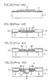
- FIGS. 3A to 3G show the steps in the manufacture of MOSFET with DSC.
- a pad oxide layer 2 and a nitride layer 3 are formed on a first conductivity type silicon substrate 1.
- the nitride layer 3 is patterned to define an active region and a first conductivity type impurity is ion-implanted to define an impurity region for channel stopper (FIG. 3A).
- LOCS local oxidation of silicon
- the silicon substrate 1 is etched to form a groove by using a photoresist film 50 and the pad oxide layer 2 as a mask. And, a first conductivity type impurity is ion-implanted to form a structure in which a channel region 5 is formed below the source/drain region 7, as shown in FIG. 3D.
- a contact hole is formed in the source/drain regions 7 by means of the mask.
- Polysilicon layers 6 are deposited, and an interlayer insulating layer 31 is formed.
- the drain region 7 is provided with a conductive layer 9 and used as a wiring electrode to obtain a complete DSC-MOSFET, as shown in FIG. 3G.
- the DSC-MOSFET made through the above- mentioned processes has remarkably excellent characteristics in short-channel effects by deeply trenching the channel region 5 compared to the source/drain regions 7 to dispose source/drain junctions on the higher position than that of the gate.
- the DSC-MOSFET made in a prior art technology has a technical difficulty of dry-etching the silicon substrate and a problem of deterioration to device performance characteristics caused by the reduction of transconductance because of damage of the substrate surface.
- the present invention seeks to solve the above problems.
- the present invention provides a method for making a metal oxide semiconductor field effect transistor, comprising the steps of:
- a method for making a metal oxide semiconductor field effect transistor comprises the steps of:
- FIGS. 1A to 1H are the steps in the manufacture of a metal oxide semiconductor field effect transistor with a channel separated from source/drain regions in accordance with the preferred embodiments of this invention.
- a first step is to define simultaneously a channel area a and field areas c.
- a pad oxide layer 2, buffer layer, and nitride layers 3, anti-oxidation layer are formed on a semiconductor substrate 1 of a predetermined conductivity type.
- the channel area a and field areas c are simultaneously defined and a high dose impurity of the same conductivity type as that of the substrate 1 is ion-implanted.
- a second step is to form impurity regions 4 for channel stopper and field oxide layers 10 by performing a local oxidation of silicon (LOCOS) process on the channel area and the field areas defined through the first step (FIG. 1 B).
- LOCS local oxidation of silicon
- a third step is to form a channel region 5.
- a gate oxide layer 20 is formed all over the substrate, and a high dose impurity of the same conductivity type as that of the substrate is ion-implanted to control a threshold voltage.
- a channel region 5 of concave shape (M) is formed, as shown in FIG. 1 C.
- the above process of the present invention does not include an additional process for defining the conventional channel regions (FIGS. 3A to 3G) and surface damage caused by dry-etching the substrate. Moreover, the impurity for controlling a threshold voltage is ion-implanted all over the substrate in the present invention, and there is no reduction of the mobility of carrier and transconductance generated in the separated region (the region "d" in FIG. 3D) between the channel and source/drain regions.
- a fourth step is to form a polysilicon gate 6 over the channel region 5 of concave shape (M) ( FIG. 1 D).
- a fifth step is to form a chemical vapor deposition (CVD) oxide layer 30 to insulate the polysilicon gate layer 6 from a metal layer that is formed through the post process.
- CVD chemical vapor deposition
- a photoresist film (not illustrated) is deposited for planarization of device, and an etch-back process is then performed to form the CVD oxide layer 30 having good step coverage, as shown in FIG. 1 E.
- This process may be deleted, if necessary.
- a sixth step is to form the source/drain regions 7 and a high dose impurity region 8 having the same conductivity type as that of the substrate 1, referring to FIGS. 1 and 1 G.
- the source/drain regions 7 are formed by implanting a high dose impurity of the different conductivity type from that of the substrate 1, after the CVD oxide layer 30 is etched by using a pattern of a photoresist film 51 as a mask.
- the above impurity region 8 is formed by using the pattern of the photoresist film 52, and the implanted impurity has the same conductivity as that of the substrate 1.
- a region of a field oxide layer indicated by letter "e" is defined simultaneously with the etch-back process and the formation of source/drain and impurity regions 7 and 8, and may be regulated and controlled in size.
- the narrow field region e may isolate electrical elements from each other.
- interlayer insulating layers 31 are opened and conductive layers 9 are provided by burying a metal on a contact hole such that a MOSFET with a drain separated from the channel region (DSC) is completely formed as shown in FIG. 1 H.
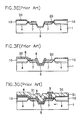
- FIGS. 2A to 2F A second embodiment of a method for making a MOSFET with a drain separated from a channel region is now described with reference to FIGS. 2A to 2F that correspond to each of FIGS. 1A to 1H, and the same description will be deleted.
- This second embodiment may reduce remarkably a bird's beak configuration of the field oxide layer compared to that of the first preferred embodiment and maintain the initial planarization of device.
- first nitride layers 3 are patterned on a first pad oxide layer 2 to define an active area a and field areas c (FIG. 2A).
- First field oxide layers 10 are formed by performing a local oxidation (LOCOS) without ion- implantation (FIG. 2B).
- LOCS local oxidation
- nitride layers 3 and field oxide layers 10 are removed, second nitride layers 3' are formed on an active region over the second pad oxide layer 2', and impurity for channel stopper is ion-implanted to form a structure of FIG. 2C.
- a second LOCOS process is carried out on the field regions defined through the above process to form impurity regions for channel stopper 4 having the same conductivity type as that of the substrate 1 and second field oxide layers 10' without the bird's beak configuration (FIG. 2D).
- a gate oxide layer 20 is formed after removal of the second nitride layers 3' and pad oxide layers 2'. Impurity of the same conductivity type as that of the substrate is ion-implanted all over the substrate 1 for controlling a threshold voltage.
- the sixth step of the first preferred embodiment and wiring process are carried out on the above structure to form a MOSFET with source/drain regions 7 separated from the concave-shaped channel regions 5, as shown in FIG. 2F.
- channel regions and field areas are defined simultaneously and a MOSFET with concave-shaped channel regions separated from a drain region is formed by using LOCOS, such that surface damage produced by etching the silicon substrate may be prevented.
- the impurity for controlling a threshold voltage is implanted all over the channel regions to prevent reduction of the mobility of carrier and transconductance that may be generated in the region where the channel regions are separated from the drain region.
- the present invention facilitates planarization of device and controls the size of each region. Accordingly, the present invention may enhance the reliability and performance of device, a basic object of MOSFET according to the scale-down.
Landscapes
- Insulated Gate Type Field-Effect Transistor (AREA)
- Element Separation (AREA)
Applications Claiming Priority (2)
| Application Number | Priority Date | Filing Date | Title |
|---|---|---|---|
| KR1019930003575A KR940022917A (ko) | 1993-03-10 | 1993-03-10 | 채널로부터 분리된 드레인을 구비한 모스에프이티(mosfet) 소자의 제조 방법 |
| KR9303575 | 1993-03-10 |
Publications (2)
| Publication Number | Publication Date |
|---|---|
| EP0615282A2 true EP0615282A2 (de) | 1994-09-14 |
| EP0615282A3 EP0615282A3 (de) | 1996-12-11 |
Family
ID=19351909
Family Applications (1)
| Application Number | Title | Priority Date | Filing Date |
|---|---|---|---|
| EP94103605A Withdrawn EP0615282A3 (de) | 1993-03-10 | 1994-03-09 | Verfahren zur Herstellung von MOSFET's mit von der Wanne gescheidenem Kanal. |
Country Status (5)
| Country | Link |
|---|---|
| EP (1) | EP0615282A3 (de) |
| JP (1) | JPH06310718A (de) |
| KR (1) | KR940022917A (de) |
| CN (1) | CN1101457A (de) |
| TW (1) | TW232087B (de) |
Cited By (4)
| Publication number | Priority date | Publication date | Assignee | Title |
|---|---|---|---|---|
| GB2354880A (en) * | 1999-09-30 | 2001-04-04 | Mitel Semiconductor Ltd | Metal oxide semiconductor field effect transistors |
| CN1103117C (zh) * | 1997-02-06 | 2003-03-12 | 日本电气株式会社 | 可用氢离子改变其阈值电压的场效应晶体管的制造工艺 |
| EP1528599A3 (de) * | 2003-10-28 | 2007-09-05 | Dongbu Electronics Co., Ltd. | Verfahren zur Herstellung einer Halbleiter-Transistoranordnung |
| JP2014175373A (ja) * | 2013-03-06 | 2014-09-22 | Ricoh Co Ltd | 半導体装置及びその製造方法 |
Families Citing this family (3)
| Publication number | Priority date | Publication date | Assignee | Title |
|---|---|---|---|---|
| JP4950648B2 (ja) * | 2006-12-15 | 2012-06-13 | セイコーインスツル株式会社 | 半導体装置およびその製造方法 |
| CN102054699B (zh) * | 2009-11-05 | 2012-07-25 | 中芯国际集成电路制造(上海)有限公司 | 改善半导体器件结深特性的方法 |
| CN112151616B (zh) * | 2020-08-20 | 2022-12-16 | 中国科学院微电子研究所 | 一种堆叠mos器件及其制备方法 |
Family Cites Families (5)
| Publication number | Priority date | Publication date | Assignee | Title |
|---|---|---|---|---|
| JPS54146584A (en) * | 1978-05-09 | 1979-11-15 | Mitsubishi Electric Corp | Manufacture of semiconductor device |
| US4903107A (en) * | 1986-12-29 | 1990-02-20 | General Electric Company | Buried oxide field isolation structure with composite dielectric |
| US5116771A (en) * | 1989-03-20 | 1992-05-26 | Massachusetts Institute Of Technology | Thick contacts for ultra-thin silicon on insulator films |
| US5108937A (en) * | 1991-02-01 | 1992-04-28 | Taiwan Semiconductor Manufacturing Company | Method of making a recessed gate MOSFET device structure |
| JPH05109762A (ja) * | 1991-05-16 | 1993-04-30 | Internatl Business Mach Corp <Ibm> | 半導体装置及びその製造方法 |
-
1993
- 1993-03-10 KR KR1019930003575A patent/KR940022917A/ko not_active Ceased
-
1994
- 1994-03-09 EP EP94103605A patent/EP0615282A3/de not_active Withdrawn
- 1994-03-09 JP JP6038385A patent/JPH06310718A/ja not_active Withdrawn
- 1994-03-10 CN CN94104276A patent/CN1101457A/zh active Pending
- 1994-03-26 TW TW083102655A patent/TW232087B/zh active
Cited By (5)
| Publication number | Priority date | Publication date | Assignee | Title |
|---|---|---|---|---|
| CN1103117C (zh) * | 1997-02-06 | 2003-03-12 | 日本电气株式会社 | 可用氢离子改变其阈值电压的场效应晶体管的制造工艺 |
| GB2354880A (en) * | 1999-09-30 | 2001-04-04 | Mitel Semiconductor Ltd | Metal oxide semiconductor field effect transistors |
| US6579765B1 (en) | 1999-09-30 | 2003-06-17 | Zarlink Semiconductor Limited | Metal oxide semiconductor field effect transistors |
| EP1528599A3 (de) * | 2003-10-28 | 2007-09-05 | Dongbu Electronics Co., Ltd. | Verfahren zur Herstellung einer Halbleiter-Transistoranordnung |
| JP2014175373A (ja) * | 2013-03-06 | 2014-09-22 | Ricoh Co Ltd | 半導体装置及びその製造方法 |
Also Published As
| Publication number | Publication date |
|---|---|
| KR940022917A (ko) | 1994-10-22 |
| CN1101457A (zh) | 1995-04-12 |
| JPH06310718A (ja) | 1994-11-04 |
| TW232087B (de) | 1994-10-11 |
| EP0615282A3 (de) | 1996-12-11 |
Similar Documents
| Publication | Publication Date | Title |
|---|---|---|
| US5510281A (en) | Method of fabricating a self-aligned DMOS transistor device using SiC and spacers | |
| US5391907A (en) | Semiconductor device with buried inverse T-type field region | |
| US5132238A (en) | Method of manufacturing semiconductor device utilizing an accumulation layer | |
| US6300207B1 (en) | Depleted sidewall-poly LDD transistor | |
| US6033959A (en) | Method of fabricating a multiple T-gate MOSFET device | |
| KR100272051B1 (ko) | 접점윈도우를통해베이스주입한p-채널mos게이트소자제조공정 | |
| US5073506A (en) | Method for making a self-aligned lateral bipolar SOI transistor | |
| JPS63281465A (ja) | 電界効果トランジスタ及びその中間体の製造方法 | |
| JPH08264789A (ja) | 絶縁ゲート半導体装置および製造方法 | |
| EP0615282A2 (de) | Verfahren zur Herstellung von MOSFET's mit von der Wanne gescheidenem Kanal | |
| JP3106757B2 (ja) | Mos電界効果半導体装置の製造方法 | |
| JPH06177377A (ja) | 絶縁ゲート電界効果トランジスタ | |
| JP2548832B2 (ja) | 半導体装置およびその製造方法 | |
| EP0081999A2 (de) | Verfahren zur Herstellung eines MOS Transistors auf einem Substrat | |
| JPS63155768A (ja) | 半導体デバイスの製造方法 | |
| US5620911A (en) | Method for fabricating a metal field effect transistor having a recessed gate | |
| KR0147428B1 (ko) | 고집적 반도체 소자 및 그 제조방법 | |
| US7015103B2 (en) | Method for fabricating vertical transistor | |
| JP3148227B2 (ja) | 半導体装置の製造方法 | |
| JP3061157B2 (ja) | 半導体素子の形成方法 | |
| JPH05129335A (ja) | 縦型トランジスタの製造方法 | |
| KR0144882B1 (ko) | 이중-확산 모스 전계 트랜지스터의 제조방법 | |
| JPH0290567A (ja) | 半導体装置とその製造方法 | |
| JPH0786586A (ja) | 半導体装置及びその製造方法 | |
| JP2531688B2 (ja) | 半導体装置の製造方法 |
Legal Events
| Date | Code | Title | Description |
|---|---|---|---|
| PUAI | Public reference made under article 153(3) epc to a published international application that has entered the european phase |
Free format text: ORIGINAL CODE: 0009012 |
|
| AK | Designated contracting states |
Kind code of ref document: A2 Designated state(s): DE FR |
|
| PUAL | Search report despatched |
Free format text: ORIGINAL CODE: 0009013 |
|
| AK | Designated contracting states |
Kind code of ref document: A3 Designated state(s): DE FR |
|
| STAA | Information on the status of an ep patent application or granted ep patent |
Free format text: STATUS: THE APPLICATION IS DEEMED TO BE WITHDRAWN |
|
| 18D | Application deemed to be withdrawn |
Effective date: 19961001 |