EP0615282A2 - Methods for making MOSFET's with drain separated from channel - Google Patents
Methods for making MOSFET's with drain separated from channel Download PDFInfo
- Publication number
- EP0615282A2 EP0615282A2 EP94103605A EP94103605A EP0615282A2 EP 0615282 A2 EP0615282 A2 EP 0615282A2 EP 94103605 A EP94103605 A EP 94103605A EP 94103605 A EP94103605 A EP 94103605A EP 0615282 A2 EP0615282 A2 EP 0615282A2
- Authority
- EP
- European Patent Office
- Prior art keywords
- layer
- region
- forming
- channel
- oxidation
- Prior art date
- Legal status (The legal status is an assumption and is not a legal conclusion. Google has not performed a legal analysis and makes no representation as to the accuracy of the status listed.)
- Withdrawn
Links
- 238000000034 method Methods 0.000 title claims abstract description 33
- 239000000758 substrate Substances 0.000 claims abstract description 23
- 239000004065 semiconductor Substances 0.000 claims abstract description 14
- 230000005669 field effect Effects 0.000 claims abstract description 13
- 229910044991 metal oxide Inorganic materials 0.000 claims abstract description 13
- 150000004706 metal oxides Chemical class 0.000 claims abstract description 13
- XUIMIQQOPSSXEZ-UHFFFAOYSA-N Silicon Chemical compound [Si] XUIMIQQOPSSXEZ-UHFFFAOYSA-N 0.000 claims abstract description 11
- 229910052710 silicon Inorganic materials 0.000 claims abstract description 11
- 239000010703 silicon Substances 0.000 claims abstract description 11
- 230000003064 anti-oxidating effect Effects 0.000 claims description 13
- 230000003647 oxidation Effects 0.000 claims description 9
- 238000007254 oxidation reaction Methods 0.000 claims description 9
- 239000000463 material Substances 0.000 claims description 8
- 238000000059 patterning Methods 0.000 claims description 4
- 239000012535 impurity Substances 0.000 abstract description 19
- 238000005530 etching Methods 0.000 abstract description 4
- 239000010410 layer Substances 0.000 description 63
- 150000004767 nitrides Chemical class 0.000 description 9
- 230000000694 effects Effects 0.000 description 7
- 238000004519 manufacturing process Methods 0.000 description 6
- 229920002120 photoresistant polymer Polymers 0.000 description 5
- 238000005229 chemical vapour deposition Methods 0.000 description 4
- 230000001276 controlling effect Effects 0.000 description 3
- 238000001312 dry etching Methods 0.000 description 3
- 229910021420 polycrystalline silicon Inorganic materials 0.000 description 3
- 229920005591 polysilicon Polymers 0.000 description 3
- 241000293849 Cordylanthus Species 0.000 description 2
- 230000005684 electric field Effects 0.000 description 2
- 239000011229 interlayer Substances 0.000 description 2
- 239000002184 metal Substances 0.000 description 2
- 230000015572 biosynthetic process Effects 0.000 description 1
- 230000006866 deterioration Effects 0.000 description 1
- 230000002708 enhancing effect Effects 0.000 description 1
- 238000005468 ion implantation Methods 0.000 description 1
- 230000001105 regulatory effect Effects 0.000 description 1
- 238000004335 scaling law Methods 0.000 description 1
Images


Classifications
-
- H—ELECTRICITY
- H01—ELECTRIC ELEMENTS
- H01L—SEMICONDUCTOR DEVICES NOT COVERED BY CLASS H10
- H01L29/00—Semiconductor devices specially adapted for rectifying, amplifying, oscillating or switching and having potential barriers; Capacitors or resistors having potential barriers, e.g. a PN-junction depletion layer or carrier concentration layer; Details of semiconductor bodies or of electrodes thereof ; Multistep manufacturing processes therefor
- H01L29/02—Semiconductor bodies ; Multistep manufacturing processes therefor
- H01L29/06—Semiconductor bodies ; Multistep manufacturing processes therefor characterised by their shape; characterised by the shapes, relative sizes, or dispositions of the semiconductor regions ; characterised by the concentration or distribution of impurities within semiconductor regions
- H01L29/10—Semiconductor bodies ; Multistep manufacturing processes therefor characterised by their shape; characterised by the shapes, relative sizes, or dispositions of the semiconductor regions ; characterised by the concentration or distribution of impurities within semiconductor regions with semiconductor regions connected to an electrode not carrying current to be rectified, amplified or switched and such electrode being part of a semiconductor device which comprises three or more electrodes
- H01L29/1025—Channel region of field-effect devices
- H01L29/1029—Channel region of field-effect devices of field-effect transistors
- H01L29/1033—Channel region of field-effect devices of field-effect transistors with insulated gate, e.g. characterised by the length, the width, the geometric contour or the doping structure
- H01L29/1037—Channel region of field-effect devices of field-effect transistors with insulated gate, e.g. characterised by the length, the width, the geometric contour or the doping structure and non-planar channel
-
- H—ELECTRICITY
- H01—ELECTRIC ELEMENTS
- H01L—SEMICONDUCTOR DEVICES NOT COVERED BY CLASS H10
- H01L29/00—Semiconductor devices specially adapted for rectifying, amplifying, oscillating or switching and having potential barriers; Capacitors or resistors having potential barriers, e.g. a PN-junction depletion layer or carrier concentration layer; Details of semiconductor bodies or of electrodes thereof ; Multistep manufacturing processes therefor
- H01L29/66—Types of semiconductor device ; Multistep manufacturing processes therefor
- H01L29/68—Types of semiconductor device ; Multistep manufacturing processes therefor controllable by only the electric current supplied, or only the electric potential applied, to an electrode which does not carry the current to be rectified, amplified or switched
- H01L29/76—Unipolar devices, e.g. field effect transistors
- H01L29/772—Field effect transistors
- H01L29/78—Field effect transistors with field effect produced by an insulated gate
-
- H—ELECTRICITY
- H01—ELECTRIC ELEMENTS
- H01L—SEMICONDUCTOR DEVICES NOT COVERED BY CLASS H10
- H01L21/00—Processes or apparatus adapted for the manufacture or treatment of semiconductor or solid state devices or of parts thereof
- H01L21/70—Manufacture or treatment of devices consisting of a plurality of solid state components formed in or on a common substrate or of parts thereof; Manufacture of integrated circuit devices or of parts thereof
- H01L21/77—Manufacture or treatment of devices consisting of a plurality of solid state components or integrated circuits formed in, or on, a common substrate
- H01L21/78—Manufacture or treatment of devices consisting of a plurality of solid state components or integrated circuits formed in, or on, a common substrate with subsequent division of the substrate into plural individual devices
- H01L21/82—Manufacture or treatment of devices consisting of a plurality of solid state components or integrated circuits formed in, or on, a common substrate with subsequent division of the substrate into plural individual devices to produce devices, e.g. integrated circuits, each consisting of a plurality of components
- H01L21/822—Manufacture or treatment of devices consisting of a plurality of solid state components or integrated circuits formed in, or on, a common substrate with subsequent division of the substrate into plural individual devices to produce devices, e.g. integrated circuits, each consisting of a plurality of components the substrate being a semiconductor, using silicon technology
- H01L21/8232—Field-effect technology
- H01L21/8234—MIS technology, i.e. integration processes of field effect transistors of the conductor-insulator-semiconductor type
- H01L21/823412—MIS technology, i.e. integration processes of field effect transistors of the conductor-insulator-semiconductor type with a particular manufacturing method of the channel structures, e.g. channel implants, halo or pocket implants, or channel materials
-
- H—ELECTRICITY
- H01—ELECTRIC ELEMENTS
- H01L—SEMICONDUCTOR DEVICES NOT COVERED BY CLASS H10
- H01L21/00—Processes or apparatus adapted for the manufacture or treatment of semiconductor or solid state devices or of parts thereof
- H01L21/70—Manufacture or treatment of devices consisting of a plurality of solid state components formed in or on a common substrate or of parts thereof; Manufacture of integrated circuit devices or of parts thereof
- H01L21/77—Manufacture or treatment of devices consisting of a plurality of solid state components or integrated circuits formed in, or on, a common substrate
- H01L21/78—Manufacture or treatment of devices consisting of a plurality of solid state components or integrated circuits formed in, or on, a common substrate with subsequent division of the substrate into plural individual devices
- H01L21/82—Manufacture or treatment of devices consisting of a plurality of solid state components or integrated circuits formed in, or on, a common substrate with subsequent division of the substrate into plural individual devices to produce devices, e.g. integrated circuits, each consisting of a plurality of components
- H01L21/822—Manufacture or treatment of devices consisting of a plurality of solid state components or integrated circuits formed in, or on, a common substrate with subsequent division of the substrate into plural individual devices to produce devices, e.g. integrated circuits, each consisting of a plurality of components the substrate being a semiconductor, using silicon technology
- H01L21/8232—Field-effect technology
- H01L21/8234—MIS technology, i.e. integration processes of field effect transistors of the conductor-insulator-semiconductor type
- H01L21/823481—MIS technology, i.e. integration processes of field effect transistors of the conductor-insulator-semiconductor type isolation region manufacturing related aspects, e.g. to avoid interaction of isolation region with adjacent structure
-
- H—ELECTRICITY
- H01—ELECTRIC ELEMENTS
- H01L—SEMICONDUCTOR DEVICES NOT COVERED BY CLASS H10
- H01L29/00—Semiconductor devices specially adapted for rectifying, amplifying, oscillating or switching and having potential barriers; Capacitors or resistors having potential barriers, e.g. a PN-junction depletion layer or carrier concentration layer; Details of semiconductor bodies or of electrodes thereof ; Multistep manufacturing processes therefor
- H01L29/66—Types of semiconductor device ; Multistep manufacturing processes therefor
- H01L29/66007—Multistep manufacturing processes
- H01L29/66075—Multistep manufacturing processes of devices having semiconductor bodies comprising group 14 or group 13/15 materials
- H01L29/66227—Multistep manufacturing processes of devices having semiconductor bodies comprising group 14 or group 13/15 materials the devices being controllable only by the electric current supplied or the electric potential applied, to an electrode which does not carry the current to be rectified, amplified or switched, e.g. three-terminal devices
- H01L29/66409—Unipolar field-effect transistors
- H01L29/66477—Unipolar field-effect transistors with an insulated gate, i.e. MISFET
- H01L29/66568—Lateral single gate silicon transistors
- H01L29/66613—Lateral single gate silicon transistors with a gate recessing step, e.g. using local oxidation
Definitions
- the present invention relates to a method for making a metal oxide semiconductor field effect transistor. More particularly, it relates to a method for making a metal oxide semiconductor field effect transistor having a recessed gate structure that may reduce short-channel effects without trench- etching and/or etching processes.
- MOSFETs metal oxide semiconductor field effect transistors
- the speed of device performance has been improved but problems of device reliability are caused.
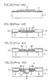
- FIGS. 3A to 3G show the steps in the manufacture of MOSFET with DSC.
- a pad oxide layer 2 and a nitride layer 3 are formed on a first conductivity type silicon substrate 1.
- the nitride layer 3 is patterned to define an active region and a first conductivity type impurity is ion-implanted to define an impurity region for channel stopper (FIG. 3A).
- LOCS local oxidation of silicon
- the silicon substrate 1 is etched to form a groove by using a photoresist film 50 and the pad oxide layer 2 as a mask. And, a first conductivity type impurity is ion-implanted to form a structure in which a channel region 5 is formed below the source/drain region 7, as shown in FIG. 3D.
- a contact hole is formed in the source/drain regions 7 by means of the mask.
- Polysilicon layers 6 are deposited, and an interlayer insulating layer 31 is formed.
- the drain region 7 is provided with a conductive layer 9 and used as a wiring electrode to obtain a complete DSC-MOSFET, as shown in FIG. 3G.
- the DSC-MOSFET made through the above- mentioned processes has remarkably excellent characteristics in short-channel effects by deeply trenching the channel region 5 compared to the source/drain regions 7 to dispose source/drain junctions on the higher position than that of the gate.
- the DSC-MOSFET made in a prior art technology has a technical difficulty of dry-etching the silicon substrate and a problem of deterioration to device performance characteristics caused by the reduction of transconductance because of damage of the substrate surface.
- the present invention seeks to solve the above problems.
- the present invention provides a method for making a metal oxide semiconductor field effect transistor, comprising the steps of:
- a method for making a metal oxide semiconductor field effect transistor comprises the steps of:
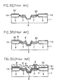
- FIGS. 1A to 1H are the steps in the manufacture of a metal oxide semiconductor field effect transistor with a channel separated from source/drain regions in accordance with the preferred embodiments of this invention.
- a first step is to define simultaneously a channel area a and field areas c.
- a pad oxide layer 2, buffer layer, and nitride layers 3, anti-oxidation layer are formed on a semiconductor substrate 1 of a predetermined conductivity type.
- the channel area a and field areas c are simultaneously defined and a high dose impurity of the same conductivity type as that of the substrate 1 is ion-implanted.
- a second step is to form impurity regions 4 for channel stopper and field oxide layers 10 by performing a local oxidation of silicon (LOCOS) process on the channel area and the field areas defined through the first step (FIG. 1 B).
- LOCS local oxidation of silicon
- a third step is to form a channel region 5.
- a gate oxide layer 20 is formed all over the substrate, and a high dose impurity of the same conductivity type as that of the substrate is ion-implanted to control a threshold voltage.
- a channel region 5 of concave shape (M) is formed, as shown in FIG. 1 C.
- the above process of the present invention does not include an additional process for defining the conventional channel regions (FIGS. 3A to 3G) and surface damage caused by dry-etching the substrate. Moreover, the impurity for controlling a threshold voltage is ion-implanted all over the substrate in the present invention, and there is no reduction of the mobility of carrier and transconductance generated in the separated region (the region "d" in FIG. 3D) between the channel and source/drain regions.
- a fourth step is to form a polysilicon gate 6 over the channel region 5 of concave shape (M) ( FIG. 1 D).
- a fifth step is to form a chemical vapor deposition (CVD) oxide layer 30 to insulate the polysilicon gate layer 6 from a metal layer that is formed through the post process.
- CVD chemical vapor deposition
- a photoresist film (not illustrated) is deposited for planarization of device, and an etch-back process is then performed to form the CVD oxide layer 30 having good step coverage, as shown in FIG. 1 E.
- This process may be deleted, if necessary.
- a sixth step is to form the source/drain regions 7 and a high dose impurity region 8 having the same conductivity type as that of the substrate 1, referring to FIGS. 1 and 1 G.
- the source/drain regions 7 are formed by implanting a high dose impurity of the different conductivity type from that of the substrate 1, after the CVD oxide layer 30 is etched by using a pattern of a photoresist film 51 as a mask.
- the above impurity region 8 is formed by using the pattern of the photoresist film 52, and the implanted impurity has the same conductivity as that of the substrate 1.
- a region of a field oxide layer indicated by letter "e" is defined simultaneously with the etch-back process and the formation of source/drain and impurity regions 7 and 8, and may be regulated and controlled in size.
- the narrow field region e may isolate electrical elements from each other.
- interlayer insulating layers 31 are opened and conductive layers 9 are provided by burying a metal on a contact hole such that a MOSFET with a drain separated from the channel region (DSC) is completely formed as shown in FIG. 1 H.
- FIGS. 2A to 2F A second embodiment of a method for making a MOSFET with a drain separated from a channel region is now described with reference to FIGS. 2A to 2F that correspond to each of FIGS. 1A to 1H, and the same description will be deleted.
- This second embodiment may reduce remarkably a bird's beak configuration of the field oxide layer compared to that of the first preferred embodiment and maintain the initial planarization of device.
- first nitride layers 3 are patterned on a first pad oxide layer 2 to define an active area a and field areas c (FIG. 2A).
- First field oxide layers 10 are formed by performing a local oxidation (LOCOS) without ion- implantation (FIG. 2B).
- LOCS local oxidation
- nitride layers 3 and field oxide layers 10 are removed, second nitride layers 3' are formed on an active region over the second pad oxide layer 2', and impurity for channel stopper is ion-implanted to form a structure of FIG. 2C.
- a second LOCOS process is carried out on the field regions defined through the above process to form impurity regions for channel stopper 4 having the same conductivity type as that of the substrate 1 and second field oxide layers 10' without the bird's beak configuration (FIG. 2D).
- a gate oxide layer 20 is formed after removal of the second nitride layers 3' and pad oxide layers 2'. Impurity of the same conductivity type as that of the substrate is ion-implanted all over the substrate 1 for controlling a threshold voltage.
- the sixth step of the first preferred embodiment and wiring process are carried out on the above structure to form a MOSFET with source/drain regions 7 separated from the concave-shaped channel regions 5, as shown in FIG. 2F.
- channel regions and field areas are defined simultaneously and a MOSFET with concave-shaped channel regions separated from a drain region is formed by using LOCOS, such that surface damage produced by etching the silicon substrate may be prevented.
- the impurity for controlling a threshold voltage is implanted all over the channel regions to prevent reduction of the mobility of carrier and transconductance that may be generated in the region where the channel regions are separated from the drain region.
- the present invention facilitates planarization of device and controls the size of each region. Accordingly, the present invention may enhance the reliability and performance of device, a basic object of MOSFET according to the scale-down.
Landscapes
- Engineering & Computer Science (AREA)
- Microelectronics & Electronic Packaging (AREA)
- Power Engineering (AREA)
- Physics & Mathematics (AREA)
- Condensed Matter Physics & Semiconductors (AREA)
- General Physics & Mathematics (AREA)
- Computer Hardware Design (AREA)
- Manufacturing & Machinery (AREA)
- Ceramic Engineering (AREA)
- Insulated Gate Type Field-Effect Transistor (AREA)
- Element Separation (AREA)
Abstract
A method for making a gooved-gate metal oxide semiconductor field effect transistor (MOSFET) with its drain separated from channel regions (DSC structure) is proposed for the purpose of meeting all the requirements of device reliability and performance that are introduced in the deep submicron technique.
According to the present invention, channel regions and field areas are defined simultaneously and a MOSFET with concave-shaped channel regions separated from a drain region is formed by using LOCOS, such that surface damage produced by etching the silicon substrate may be prevented. The impurity for controlling a threshold voltage is implanted all over the channel regions to prevent reduction of the mobility of carrier and transconductance that may be generated in the region where the channel regions are separated from the drain region.
Description
- The present invention relates to a method for making a metal oxide semiconductor field effect transistor. More particularly, it relates to a method for making a metal oxide semiconductor field effect transistor having a recessed gate structure that may reduce short-channel effects without trench- etching and/or etching processes.
- For past years, manufacturing techniques of metal oxide semiconductor field effect transistors (MOSFETs) have been rapidly developed, reducing the minimum size of structural elements of integrated circuits by the ratio of about 10%. This trend is expected to continue in 1990's. Thus, the size of a MOSFET (gate length Lg orchannel length) has been reduced to a deep submicron region (Lg<0.35um) from a submicron region (Lg<1I.Lm) for the increase of device performance and integrity. However, as the size of a MOSFET is reduced to the submicron region, it is difficult to suit best short-channel effects, hot carrier effects, and device characteristics altogether, according to the reduction of electric field.
- According to the scaling law, the speed of device performance has been improved but problems of device reliability are caused. The limit to the size of voltages placed is resulted not from short-channel effects such as simple punchthrough voltages but from the reduction of device reliability by the increase of energy carrier (or increase of temperatures, E = 3/2kT) due to the increase of electric fields inside the channel.
- From the late in the 1980's, the study on MOSFETs has been focused on the limit of device by scaling and the scaling limit by device reliability. Besides, there has been studied a structure that may moderate the scaling limit, by enhancing the device reliability. According to KITE REVIEW, Vol. 19 No. 5 pp 402 - 413, the device cannot be totally turned off at gate voltages Vg = OV by short-channel effects.
- In such a technological background, there is a structure in which channel regions are not formed on the same plane as that of source/drain regions in order to overcome the limit of short-channel effects. EIJI TAKEDA et al referred to such a structure "MOSFET with Drain Separated from Channel Implanted Region (DSC)" in IEEE Ttans. Electron Devices, Vol. 30, No. 6, 1983.
- FIGS. 3A to 3G show the steps in the manufacture of MOSFET with DSC.
- First, a
pad oxide layer 2 and anitride layer 3 are formed on a first conductivitytype silicon substrate 1. Thenitride layer 3 is patterned to define an active region and a first conductivity type impurity is ion-implanted to define an impurity region for channel stopper (FIG. 3A). - After that, a local oxidation of silicon (LOCOS) process is performed to form a
field oxide layer 10, and thenitride layer 3 is then removed. A source/drain region 7 is formed by ion-implanting second conductivity type impurity with high dosage, as shown in FIG. 3B. - Referring now to FIG. 3C, the
silicon substrate 1 is etched to form a groove by using aphotoresist film 50 and thepad oxide layer 2 as a mask. And, a first conductivity type impurity is ion-implanted to form a structure in which achannel region 5 is formed below the source/drain region 7, as shown in FIG. 3D. - As shown in FIGS. 3E to 3G, after the
photoresist film 50 andpad oxide layer 2 are removed, andgate oxide layers 20 are formed, a contact hole is formed in the source/drain regions 7 by means of the mask.Polysilicon layers 6 are deposited, and aninterlayer insulating layer 31 is formed. Thedrain region 7 is provided with aconductive layer 9 and used as a wiring electrode to obtain a complete DSC-MOSFET, as shown in FIG. 3G. - The DSC-MOSFET made through the above- mentioned processes, has remarkably excellent characteristics in short-channel effects by deeply trenching the
channel region 5 compared to the source/drain regions 7 to dispose source/drain junctions on the higher position than that of the gate. However, the DSC-MOSFET made in a prior art technology has a technical difficulty of dry-etching the silicon substrate and a problem of deterioration to device performance characteristics caused by the reduction of transconductance because of damage of the substrate surface. - Besides, since the impurity is not fully implanted to a region "d", a separated region between the
channel region 5 and source/drain regions 7, the mobility of carrier is reduced, which deteriorates current driving capability at last. - The present invention seeks to solve the above problems.
- It is an object of this invention to provide a method for making a metal oxide semiconductor field effect transistor that can meet all the requirements of reliability and performance as well, by solving a difficulty of dry-etching a substrate and forming channel regions to be separated from source/drain regions.
- The present invention provides a method for making a metal oxide semiconductor field effect transistor, comprising the steps of:
- forming a buffer layer and an anti-oxidation layer on a silicon substrate to define simultaneously channel and field areas;
- forming field oxide layers through an oxidation process;
- removing the buffer layer, anti-oxidation layer and field oxide layer to form a concave-shaped channel region;
- forming a gate insulating layer and a gate material layer and patterning the gate material layer; and
- forming source/drain regions and a region of field oxide layer.
- According to another aspect of the present invention, a method for making a metal oxide semiconductor field effect transistor, comprises the steps of:
- forming a first buffer layer and a first anti-oxidation layer on a silicon substrate to define simultaneously channel and field areas;
- forming first field oxide layers through a first oxidation process;
- removing the first buffer layer, first anti-oxidation layer and first field oxide layer to form a concave-shaped channel region;
- forming a second buffer and a second anti-oxidation layer, and removing the second anti-oxidation layer in the field region;
- forming second field oxide layers through a second oxidation process;
- forming a gate insulating layer and a gate material layer, and patterning the gate material layer; and
- forming source/drain regions.
-
- FIGS. 1A to 1H depict the steps in the manufacture of a metal oxide semiconductor field effect transistor in accordance with a first preferred embodiment of this invention;
- FIGS. 2A to 2F depict the steps in the manufacture of a metal oxide semiconductor field effect transistor in accordance with a second preferred embodiment of this invention; and
- FIGS. 3A to 3G depict the steps in the manufacture of a metal oxide semiconductor field effect transistor in a conventional way.
- Preferred embodiments of the present invention are now fully described with reference to the attached drawings.
- FIGS. 1A to 1H are the steps in the manufacture of a metal oxide semiconductor field effect transistor with a channel separated from source/drain regions in accordance with the preferred embodiments of this invention.
- Referring now to FIG. 1A, a first step is to define simultaneously a channel area a and field areas c. First, a
pad oxide layer 2, buffer layer, andnitride layers 3, anti-oxidation layer are formed on asemiconductor substrate 1 of a predetermined conductivity type. The channel area a and field areas c are simultaneously defined and a high dose impurity of the same conductivity type as that of thesubstrate 1 is ion-implanted. - At this point, source/drain regions will be formed in an area "b". A second step is to form
impurity regions 4 for channel stopper and field oxide layers 10 by performing a local oxidation of silicon (LOCOS) process on the channel area and the field areas defined through the first step (FIG. 1 B). - A third step is to form a
channel region 5. After thepad oxide layers 2,nitride layers 3 and field oxide layers 10 are completely removed, agate oxide layer 20 is formed all over the substrate, and a high dose impurity of the same conductivity type as that of the substrate is ion-implanted to control a threshold voltage. Achannel region 5 of concave shape (M) is formed, as shown in FIG. 1 C. - The above process of the present invention does not include an additional process for defining the conventional channel regions (FIGS. 3A to 3G) and surface damage caused by dry-etching the substrate. Moreover, the impurity for controlling a threshold voltage is ion-implanted all over the substrate in the present invention, and there is no reduction of the mobility of carrier and transconductance generated in the separated region (the region "d" in FIG. 3D) between the channel and source/drain regions.
- A fourth step is to form a
polysilicon gate 6 over thechannel region 5 of concave shape (M) ( FIG. 1 D). - A fifth step is to form a chemical vapor deposition (CVD)
oxide layer 30 to insulate thepolysilicon gate layer 6 from a metal layer that is formed through the post process. In the present invention, a photoresist film (not illustrated) is deposited for planarization of device, and an etch-back process is then performed to form theCVD oxide layer 30 having good step coverage, as shown in FIG. 1 E. - This process may be deleted, if necessary.
- A sixth step is to form the source/
drain regions 7 and a highdose impurity region 8 having the same conductivity type as that of thesubstrate 1, referring to FIGS. 1 and 1 G. The source/drain regions 7 are formed by implanting a high dose impurity of the different conductivity type from that of thesubstrate 1, after theCVD oxide layer 30 is etched by using a pattern of aphotoresist film 51 as a mask. Theabove impurity region 8 is formed by using the pattern of thephotoresist film 52, and the implanted impurity has the same conductivity as that of thesubstrate 1. A region of a field oxide layer indicated by letter "e" is defined simultaneously with the etch-back process and the formation of source/drain andimpurity regions - The narrow field region e may isolate electrical elements from each other. Finally,
interlayer insulating layers 31 are opened andconductive layers 9 are provided by burying a metal on a contact hole such that a MOSFET with a drain separated from the channel region (DSC) is completely formed as shown in FIG. 1 H. - A second embodiment of a method for making a MOSFET with a drain separated from a channel region is now described with reference to FIGS. 2A to 2F that correspond to each of FIGS. 1A to 1H, and the same description will be deleted. This second embodiment may reduce remarkably a bird's beak configuration of the field oxide layer compared to that of the first preferred embodiment and maintain the initial planarization of device.
- Like the first preferred embodiment,
first nitride layers 3 are patterned on a firstpad oxide layer 2 to define an active area a and field areas c (FIG. 2A). First field oxide layers 10 are formed by performing a local oxidation (LOCOS) without ion- implantation (FIG. 2B). - Subsequently, after the first
pad oxide layers 2,nitride layers 3 and field oxide layers 10 are removed, second nitride layers 3' are formed on an active region over the second pad oxide layer 2', and impurity for channel stopper is ion-implanted to form a structure of FIG. 2C. - A second LOCOS process is carried out on the field regions defined through the above process to form impurity regions for
channel stopper 4 having the same conductivity type as that of thesubstrate 1 and second field oxide layers 10' without the bird's beak configuration (FIG. 2D). - Referring now to FIG. 2E, a
gate oxide layer 20 is formed after removal of the second nitride layers 3' and pad oxide layers 2'. Impurity of the same conductivity type as that of the substrate is ion-implanted all over thesubstrate 1 for controlling a threshold voltage. - The sixth step of the first preferred embodiment and wiring process are carried out on the above structure to form a MOSFET with source/
drain regions 7 separated from the concave-shapedchannel regions 5, as shown in FIG. 2F. - As described above, according to the present invention, channel regions and field areas are defined simultaneously and a MOSFET with concave-shaped channel regions separated from a drain region is formed by using LOCOS, such that surface damage produced by etching the silicon substrate may be prevented. The impurity for controlling a threshold voltage is implanted all over the channel regions to prevent reduction of the mobility of carrier and transconductance that may be generated in the region where the channel regions are separated from the drain region.
- Besides, the present invention facilitates planarization of device and controls the size of each region. Accordingly, the present invention may enhance the reliability and performance of device, a basic object of MOSFET according to the scale-down.
Claims (3)
1. A method for making a metal oxide semiconductor field effect transistor, comprising the steps of:
forming a buffer layer and an anti-oxidation layer on a silicon substrate to define simultaneously channel and field areas;
forming field oxide layers through an oxidation process;
removing said buffer layer, anti-oxidation layer and field oxide layer to form a concave-shaped channel region;
forming a gate insulating layer and a gate material layer and patterning said gate material layer; and
forming source/drain regions and a region of field oxide layer.
2. A method according to claim 1, wherein said step for forming said region of field oxide layer further includes an etch-back process for planarization of a device.
3. A method for making a metal oxide semiconductor field effect transistor, comprising the steps of:
forming a first buffer layer and a first anti-oxidation layer on a silicon substrate to define simultaneously channel and field areas;
forming first field oxide layers through a first oxidation process;
removing said first buffer layer, first anti-oxidation layer and first field oxide layer to form a concave-shaped channel region;
forming a second buffer and a second anti-oxidation layer, and removing the second anti-oxidation layer in the field region;
forming second field oxide layers through a second oxidation process;
forming a gate insulating layer and a gate material layer, and patterning said gate material layer; and
forming source/drain regions.
Applications Claiming Priority (2)
| Application Number | Priority Date | Filing Date | Title |
|---|---|---|---|
| KR1019930003575A KR940022917A (en) | 1993-03-10 | 1993-03-10 | Method for manufacturing MOSFET having a drain separated from the channel |
| KR9303575 | 1993-03-10 |
Publications (2)
| Publication Number | Publication Date |
|---|---|
| EP0615282A2 true EP0615282A2 (en) | 1994-09-14 |
| EP0615282A3 EP0615282A3 (en) | 1996-12-11 |
Family
ID=19351909
Family Applications (1)
| Application Number | Title | Priority Date | Filing Date |
|---|---|---|---|
| EP94103605A Withdrawn EP0615282A3 (en) | 1993-03-10 | 1994-03-09 | Methods for making MOSFET's with drain separated from channel. |
Country Status (5)
| Country | Link |
|---|---|
| EP (1) | EP0615282A3 (en) |
| JP (1) | JPH06310718A (en) |
| KR (1) | KR940022917A (en) |
| CN (1) | CN1101457A (en) |
| TW (1) | TW232087B (en) |
Cited By (4)
| Publication number | Priority date | Publication date | Assignee | Title |
|---|---|---|---|---|
| GB2354880A (en) * | 1999-09-30 | 2001-04-04 | Mitel Semiconductor Ltd | Metal oxide semiconductor field effect transistors |
| CN1103117C (en) * | 1997-02-06 | 2003-03-12 | 日本电气株式会社 | Manufacturing engineering for field effect transistor capable of changing its threshold voltage by hydrion |
| EP1528599A2 (en) * | 2003-10-28 | 2005-05-04 | Dongbu Electronics Co., Ltd. | Method for fabricating a semiconductor transistor device |
| JP2014175373A (en) * | 2013-03-06 | 2014-09-22 | Ricoh Co Ltd | Semiconductor device and manufacturing method of the same |
Families Citing this family (3)
| Publication number | Priority date | Publication date | Assignee | Title |
|---|---|---|---|---|
| JP4950648B2 (en) * | 2006-12-15 | 2012-06-13 | セイコーインスツル株式会社 | Semiconductor device and manufacturing method thereof |
| CN102054699B (en) * | 2009-11-05 | 2012-07-25 | 中芯国际集成电路制造(上海)有限公司 | Method for improving junction depth property of semiconductor device |
| CN112151616B (en) * | 2020-08-20 | 2022-12-16 | 中国科学院微电子研究所 | Stacked MOS device and preparation method thereof |
Citations (5)
| Publication number | Priority date | Publication date | Assignee | Title |
|---|---|---|---|---|
| JPS54146584A (en) * | 1978-05-09 | 1979-11-15 | Mitsubishi Electric Corp | Manufacture of semiconductor device |
| US4903107A (en) * | 1986-12-29 | 1990-02-20 | General Electric Company | Buried oxide field isolation structure with composite dielectric |
| US5108937A (en) * | 1991-02-01 | 1992-04-28 | Taiwan Semiconductor Manufacturing Company | Method of making a recessed gate MOSFET device structure |
| US5116771A (en) * | 1989-03-20 | 1992-05-26 | Massachusetts Institute Of Technology | Thick contacts for ultra-thin silicon on insulator films |
| EP0513639A2 (en) * | 1991-05-16 | 1992-11-19 | International Business Machines Corporation | Semiconductor field effect transistor device and fabrication thereof |
-
1993
- 1993-03-10 KR KR1019930003575A patent/KR940022917A/en not_active Application Discontinuation
-
1994
- 1994-03-09 JP JP6038385A patent/JPH06310718A/en not_active Withdrawn
- 1994-03-09 EP EP94103605A patent/EP0615282A3/en not_active Withdrawn
- 1994-03-10 CN CN94104276A patent/CN1101457A/en active Pending
- 1994-03-26 TW TW083102655A patent/TW232087B/zh active
Patent Citations (5)
| Publication number | Priority date | Publication date | Assignee | Title |
|---|---|---|---|---|
| JPS54146584A (en) * | 1978-05-09 | 1979-11-15 | Mitsubishi Electric Corp | Manufacture of semiconductor device |
| US4903107A (en) * | 1986-12-29 | 1990-02-20 | General Electric Company | Buried oxide field isolation structure with composite dielectric |
| US5116771A (en) * | 1989-03-20 | 1992-05-26 | Massachusetts Institute Of Technology | Thick contacts for ultra-thin silicon on insulator films |
| US5108937A (en) * | 1991-02-01 | 1992-04-28 | Taiwan Semiconductor Manufacturing Company | Method of making a recessed gate MOSFET device structure |
| EP0513639A2 (en) * | 1991-05-16 | 1992-11-19 | International Business Machines Corporation | Semiconductor field effect transistor device and fabrication thereof |
Non-Patent Citations (1)
| Title |
|---|
| PATENT ABSTRACTS OF JAPAN vol. 004, no. 005 (E-165), 16 January 1980 & JP 54 146584 A (MITSUBISHI ELECTRIC CORP), 15 November 1979, * |
Cited By (6)
| Publication number | Priority date | Publication date | Assignee | Title |
|---|---|---|---|---|
| CN1103117C (en) * | 1997-02-06 | 2003-03-12 | 日本电气株式会社 | Manufacturing engineering for field effect transistor capable of changing its threshold voltage by hydrion |
| GB2354880A (en) * | 1999-09-30 | 2001-04-04 | Mitel Semiconductor Ltd | Metal oxide semiconductor field effect transistors |
| US6579765B1 (en) | 1999-09-30 | 2003-06-17 | Zarlink Semiconductor Limited | Metal oxide semiconductor field effect transistors |
| EP1528599A2 (en) * | 2003-10-28 | 2005-05-04 | Dongbu Electronics Co., Ltd. | Method for fabricating a semiconductor transistor device |
| EP1528599A3 (en) * | 2003-10-28 | 2007-09-05 | Dongbu Electronics Co., Ltd. | Method for fabricating a semiconductor transistor device |
| JP2014175373A (en) * | 2013-03-06 | 2014-09-22 | Ricoh Co Ltd | Semiconductor device and manufacturing method of the same |
Also Published As
| Publication number | Publication date |
|---|---|
| EP0615282A3 (en) | 1996-12-11 |
| TW232087B (en) | 1994-10-11 |
| CN1101457A (en) | 1995-04-12 |
| KR940022917A (en) | 1994-10-22 |
| JPH06310718A (en) | 1994-11-04 |
Similar Documents
| Publication | Publication Date | Title |
|---|---|---|
| US5510281A (en) | Method of fabricating a self-aligned DMOS transistor device using SiC and spacers | |
| US5391907A (en) | Semiconductor device with buried inverse T-type field region | |
| US5132238A (en) | Method of manufacturing semiconductor device utilizing an accumulation layer | |
| US6300207B1 (en) | Depleted sidewall-poly LDD transistor | |
| US6033959A (en) | Method of fabricating a multiple T-gate MOSFET device | |
| KR100272051B1 (en) | Process for manufacture of a p-channel mos gated device with base implant through the contact window | |
| US5073506A (en) | Method for making a self-aligned lateral bipolar SOI transistor | |
| JPS63281465A (en) | Manufacture of field effect transistor and its intermediate product | |
| JPH08264789A (en) | Insulated gate semiconductor device and manufacture | |
| EP0615282A2 (en) | Methods for making MOSFET's with drain separated from channel | |
| KR19980020943A (en) | Insulation tunneling transistor and manufacturing method thereof | |
| JP3106757B2 (en) | Method for manufacturing MOS field effect semiconductor device | |
| JPH06177377A (en) | Insulated-gate field-effect transistor | |
| JP2548832B2 (en) | Semiconductor device and manufacturing method thereof | |
| EP0081999A2 (en) | A method of fabricating a MOS transistor on a substrate | |
| JPS63155768A (en) | Manufacture of semiconductor device | |
| US5620911A (en) | Method for fabricating a metal field effect transistor having a recessed gate | |
| KR0147428B1 (en) | High integrated semiconductor device and the manufacturing method thereof | |
| US7015103B2 (en) | Method for fabricating vertical transistor | |
| JP3148227B2 (en) | Method for manufacturing semiconductor device | |
| JP3061157B2 (en) | Method for forming semiconductor device | |
| KR0144882B1 (en) | Method of manufacturing double-diffusion MOS field transistor | |
| JP2531688B2 (en) | Method for manufacturing semiconductor device | |
| JPH0290567A (en) | Semiconductor device and manufacture thereof | |
| KR100257709B1 (en) | Method for manufacturing transistor soi device |
Legal Events
| Date | Code | Title | Description |
|---|---|---|---|
| PUAI | Public reference made under article 153(3) epc to a published international application that has entered the european phase |
Free format text: ORIGINAL CODE: 0009012 |
|
| AK | Designated contracting states |
Kind code of ref document: A2 Designated state(s): DE FR |
|
| PUAL | Search report despatched |
Free format text: ORIGINAL CODE: 0009013 |
|
| AK | Designated contracting states |
Kind code of ref document: A3 Designated state(s): DE FR |
|
| STAA | Information on the status of an ep patent application or granted ep patent |
Free format text: STATUS: THE APPLICATION IS DEEMED TO BE WITHDRAWN |
|
| 18D | Application deemed to be withdrawn |
Effective date: 19961001 |