EP0612074B1 - Spalten-Redundanz-Schaltungsanordnung für einen Speicher - Google Patents
Spalten-Redundanz-Schaltungsanordnung für einen Speicher Download PDFInfo
- Publication number
- EP0612074B1 EP0612074B1 EP93102667A EP93102667A EP0612074B1 EP 0612074 B1 EP0612074 B1 EP 0612074B1 EP 93102667 A EP93102667 A EP 93102667A EP 93102667 A EP93102667 A EP 93102667A EP 0612074 B1 EP0612074 B1 EP 0612074B1
- Authority
- EP
- European Patent Office
- Prior art keywords
- column
- memory
- redundant
- address
- log
- Prior art date
- Legal status (The legal status is an assumption and is not a legal conclusion. Google has not performed a legal analysis and makes no representation as to the accuracy of the status listed.)
- Expired - Lifetime
Links
Images


Classifications
-
- G—PHYSICS
- G11—INFORMATION STORAGE
- G11C—STATIC STORES
- G11C29/00—Checking stores for correct operation ; Subsequent repair; Testing stores during standby or offline operation
- G11C29/70—Masking faults in memories by using spares or by reconfiguring
- G11C29/78—Masking faults in memories by using spares or by reconfiguring using programmable devices
- G11C29/83—Masking faults in memories by using spares or by reconfiguring using programmable devices with reduced power consumption
-
- G—PHYSICS
- G11—INFORMATION STORAGE
- G11C—STATIC STORES
- G11C29/00—Checking stores for correct operation ; Subsequent repair; Testing stores during standby or offline operation
- G11C29/70—Masking faults in memories by using spares or by reconfiguring
- G11C29/78—Masking faults in memories by using spares or by reconfiguring using programmable devices
- G11C29/781—Masking faults in memories by using spares or by reconfiguring using programmable devices combined in a redundant decoder
Definitions
- the invention relates to a column redundancy circuit arrangement for a memory according to the preamble of the claim 1.
- the memory cells When storing larger capacity, the memory cells divided into several blocks. Because of the matrix-like arrangement of the memory cells, the additional cells must also arranged in rows and columns. This redundant Lines are generally on the edge of the cell fields educated. They are each programmable Element related to the created Addresses selected.
- programmable elements can e.g. laser separable Be fuselocks.
- every fuseblock becomes one or several redundant lines. Should the number of repairs must be increased of the redundant lines and thus also the number the fuselocks are enlarged.
- the space requirement of one such redundancy increase is essential and can lead to a reduction in the number of pieces per disc.
- the one needed Area for the fuse blocks together with their control circuits about the size of the area that the use redundant memory cells.
- a statistic of the redundancy utilization e.g. at a 4 mega memory that on average only half of the Fuse blocks can be used for repair.
- a Doubling the redundancy allows up to 20% more yield. This shows that the previous interpretation of the Redundancy architecture, an essential part of storage cannot be repaired, although in principle enough programmable coding elements are available.
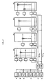
- FIG. 1 A simplified block diagram of a memory with Column redundancy, according to the prior art, is in Figure 1 shown.
- the coding units are for the redundant ones Columns assigned non-blocking.
- Figure 1 shows one Control unit CTRL which controls the external control clock RAS (Row-Address-Strobe), CAS (Column-Address-Strobe), WE (Write Enable) and possibly OE (Output Enable) processed.
- RAS Row-Address-Strobe
- CAS Columnumn-Address-Strobe
- WE Write Enable
- OE Output Enable
- a row address buffer unit is RABF shown, which from the external addresses EXAO ... q internal Row addresses RAB under the control of control lines derived from the unit CTRL.
- one Column address buffer unit CABF represented that the external addresses EXAO ... q together with control lines internal column addresses from the control unit CTRL CAB generated.
- An input-output unit IOB is provided those for data transfer to and from memory worries.
- External data lines EXDO ... p are connected to it.
- a memory block BK n consists of a cell array with a known matrix-type arrangement of memory cells, word lines WL 1, n ... WL x, n and bit line pairs BLG 1, n ... BLG y, n , where, for example, a "folded bitline" Arrangement BL, / BL is shown, from a block decoder BKDEC and a word decoder / driver RDEC 1 ... n , further from bit amplifiers / switches BS 1, n BS y, n and finally from data bit amplifiers / switches DSW 1 ... n (1 ⁇ n ⁇ N).
- a single memory block is activated by its associated block decoder BKDEC n .
- a first part of the row addresses RAB is supplied to the block decoders BKDEC n .
- These addresses are so numerous that a 1 out of N selection can be made.
- the block selection line BKS n of a selected block decoder BKDEC n activates the associated word decoder / driver RDEC n and the data bit amplifier / switch DSW n .
- the word lines of a memory block BK n are selected by the active word decoder / driver RDEC n , to which the second part of the row addresses is supplied for this purpose. Redundant word lines are not shown here.
- the signals of the bit line pairs BLG y, n are amplified by the activated bit amplifier DSW n and switched in groups by means of bit switches BS y, n to the block data bus BKDB n of the corresponding width. These bit switches are each operated by an active bit group selection line CSL 1 ... Y from the common column decoder CDEC.
- the column decoder CDEC also has a control input CFR. If this signal is inactive, ie if it is, for example, logic "0" with positive logic, all selection lines are deactivated.
- the data on the block data bus BKDB n are amplified during a read cycle and switched to the input-output bus IOBS via the data bit switches from DSW n .
- This bus 10BS connects the data bit switch DSW n to the input-output buffer 10B.
- the data from the input-output bus are written IOBS this switch on the Block Scheme BKDB n and the selected bit switches BS y, n stored in the respective cells in a write cycle.
- two redundant bit line groups RBLG 1.1 ... 2.2 with their associated bit amplifiers / switches RBS 1.1 ... 2.2 are also shown. These bit switch groups are each activated by a redundant selection line RCSL 1 or RCSL 2 from the redundant drivers RCD 1 or RCD 2 common to all memory blocks BK n .
- the function of a redundant unit is identical to that of a normal unit.
- FIG. 1 also shows two groups of N coding elements CF 1 ... N, 1 ... 2 each, ie one element per memory block BK nT and per redundant selection line RCSL 1 or RCSL 2 .
- These coding elements CF n, 1 ... 2 receive as input the first part of the row addresses RAB, which is responsible for block decoding 1 from N, and the same column addresses CAB as the column decoder CDEC. Their outputs are connected on two separate lines; CF 1 ... N, 1 on RD 1 or CF 1 ... N, 2 on RD 2 . These lines are fed to the inputs of the redundant drivers RCD 1 or RCD 2 and a NOR gate. The output of the NOR gate forms the input CFR of the column decoder.
- a memory block BK n is activated by the corresponding block decoder BKDEC n.
- the two associated coding elements CF n, 1 and CF n, 2 are also selected with the same row-address combination.
- the lines RD 1 and RD 2 are normally inactive, for example logical "0". Accordingly, the redundant failure lines RCSL 1 and RCSL 2 are also inactive, and the control signal CFR, here logical "1", enables the column decoder CDEC.
- a failure line CSLi corresponding to the column addresses CAB is therefore selected and switches a normal bit line group BLG y, n on the block data bus BKDB n of the active memory block BK n .
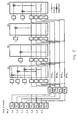
- the faulty units are marked with the letters AG.
- In the first block three errors occur A, B, C, in the second and third errors D and E respectively and in the last block two F and G.
- On the left side of FIG. 2 is the utilization of the coding elements CF1,1. .CF4.2 shown. Since only two defective units can be repaired per memory block BK1 ... 4, it is clear that in this example the memory cannot be repaired, although two unused decoding elements remain, since only six of the eight coding elements CF 1, CF 1, 1 ... 4.2 can be used. Faulty places in the memory blocks BK1 ... 4 are marked with a cross. The defective units replaced by redundant bit line groups are marked with a circle.
- FIG. 3 shows a conventional circuit according to the prior art for coding the column addresses in the case of non-blocking column redundancy in the event that laser-separable fuse blocks are used as coding elements in the circuit arrangement according to FIG.
- the two groups of coding elements mentioned above have an identical structure and are represented as units E 1 and E 2 , only one being shown in detail.
- Such a unit E 1 consists of N identical circuits CF 1 ... N, 1 for E 1 or CF 1 ... N, 2 for E 2 and a NAND gate NGN with N inputs RDN 1 ... N and an output RD 1 at E 1 or RD 2 at E 2 .
- the two output signals RD 1 and RD 2 are each fed to a redundant driver RCD 1 or RCD 2 with the outputs RCSL 1 or RCSL 2 and the gate NOR already shown in FIG.
- the output of this gate NOR is connected to a driver CFRD, the output of which is the signal CFR.
- These three drivers consist of a NAND gate and a downstream inverter.
- the second input of these NAND gates is connected to an enable signal FR which, in the case of a logic "0" state, keeps both the normal and the redundant selection lines at logic "0" at a low potential. This release signal FR is usually used for synchronization purposes.
- Such a circuit CF i, j consists of a NAND gate NGN with M inputs, a downstream inverter P1, N1, and 2 x K N-channel transistors in series, each with a fuse element, which are connected to the output A of the inverter P1, N1 connected in parallel and from an output inverter IV.
- the block selection takes place via the input NAND gate NGN, which, for example, is one of all possible combinations of M lines from the M block address lines X 1 ... M and their complementary lines / X 1 ... M is supplied.
- a circuit CF i, j is activated when all inputs of this NAND gate are logic "1".
- EP 0 492 099 also represents such a circuit.
- a disadvantage of the solution described is that when a non-programmed column address is created, ie in Y-1 cases of Y, a cross current flows across the transistor P1 of the selected circuit CF i, j after the low potential in the entire active cycle. This cross current may occur twice in each memory block group E 1 , E 2 and takes on an impermissibly high value in the case of concrete solutions with several such groups.
- Another disadvantage is, also in specific cases, the excessive number of lines RDN 1 ... N and the resulting disadvantageously large output gate NGN.
- the object of the present invention is an improved Utilization of the existing fuselocks in the enlargement of column redundancy and a reduction in To allow electricity consumption.
- FIG. 4 shows, as an example of an implementation of the block-free column redundancy according to the invention, the simplified block diagram of a memory with the same basic organization as in FIG. 1.
- each memory block BK N contains, for example, twice the number of redundant bit line groups RBL-G 1, n .. .4, n and bit amplifiers / switches RBS 1, n ... 4, n .
- the four redundant selection lines RCSL 1 ... 4 are operated by four redundant drivers RCD 1 ... 4 common to all memory blocks.
- a memory block BK n is activated with a specific row-address combination.
- Lines RD 1 ... 4 are normally inactive and, accordingly, the redundant failure lines RCSL 1 ... 4 .
- the control signal CFR is therefore logic "1" and activates the column decoder CDEC. If a addressed memory cell of the bit line group BLGy, n is defective in the memory block BK n , a coding element CF i, j is programmed for the corresponding block and column addresses. When this block address occurs, the coding element CF i, j programmed for this is selected and the line RD j is activated when the corresponding column address is created.
- the thereby inactive control signal CFR blocks the column decoder CDEC and the redundant line RCSL j is operated instead of the selection line CSL y .
- the total number of possible repairs remains 2 x N as in the first solution.
- this new solution up to four such elements CF i, 1 ... 4 are available for repair purposes per memory block.
- the space requirement for the redundant bit line groups BLG y, n is the same as when the column redundancy of the first solution is doubled.
- the number of memory blocks BK n is generally much smaller than the number of selection lines CSL y , only a few additional addresses need to be programmable for the modified coding elements CF i, j .
- FIG. 5 shows a repair example with block-free column redundancy for the same arrangement as in FIG. 2. In this case, the memory can obviously be repaired.
- the same elements in FIG. 2 and FIG. 5 have the same designation. 5, in contrast to FIG. 2, block-independent coding elements CF 1.1 ... CF 2.4 and here four redundant drivers RCD 1 ... RCD 4 are provided, in contrast to FIG. Defective storage cells are again symbolically marked with a cross and those that have been repaired are outlined with a circle.
- FIG. 1 and FIG. 4 each show a redundancy arrangement in which n coding elements CF i, j can be assigned to each active memory block BK.
- the same block address bus CAB, RAB, CTB, which is responsible for the memory block decoding, is fed to these coding elements CF i, j .
- the coding elements CF i, j are assigned to a plurality of memory blocks simultaneously. Only a subset of the block addresses is then supplied to these coding elements. A defective bit line group is replaced in all of these memory blocks simultaneously and regardless of the memory block in which a defect is actually located.
- a memory block BK n can be understood as a group of Q individual memory blocks BK n, 1... Q in the sense of the invention without any restriction.
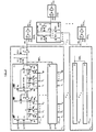
- FIG. 6 shows a circuit according to the invention for coding the column addresses in the case of block-free column redundancy with fuse blocks as coding elements.
- the input of the inverter IE is a line RDNj common to all P circuits.
- the transistors PE1 and PE2 are connected between the high potential (VDD) and this line.
- the structure and function of these drivers are the same as in FIG. 3.
- the circuit DNOR consists of two P-channel transistors PD1 and PD2 connected in parallel between the high potential VDD and a node D, and four N-channel transistors ND 1..4 connected in parallel between the node D and the low potential VSS. and from an inverter ID with input signal D.
- the gate of PD1 is connected to the signal ATDN.
- the output of ID is connected to the gate of PD2 in a retention configuration.
- the gates of the transistors ND 1..4 are connected to the lines RD 1..4 .
- Such a circuit consists of two P-channel transistors P1 and P2 connected in series, and of an N-channel transistor N1.
- the enable signal EN is connected to the gates of P1 and N1 and the set signal SP is connected to the gate of P2.
- the common connection A between P2 and N1 is the input of an inverter IV with a P-channel transistor P3 in a retention configuration.
- 2xM N-channel transistors TX 1 ... M , TNX 1 ... M are also connected in series with one fuse element FX 1 ...
- the gates of these transistors are connected to the row addresses X 1..M and / X 1..M .
- the output B of the inverter IV is connected to the gates of the P-channel transistor P4 and the N-channel transistor N2.
- a further P-channel transistor P5 with a gate signal ATDN is located between these transistors.
- the common terminal C between N2 and P5 is the input of a pull-down N-channel transistor N3, the drain output of which is connected to the common line RDN j .
- a last P-channel transistor P6 is connected at the common connection between P4 and P5 and at connection C. Its gate is connected to the output line RDN j in a restraint configuration.
- 2xK N-channel transistors TY 1 ... K , TNY 1 ... K are connected in series with a fuse element FY 1 ... K , FNY 1 ... K in parallel at connection C.
- the gates of these transistors are connected to the column addresses Y 1..K and / Y 1..K .
- the function of the circuit described is based on the Time diagram of Figure 7 explained, only the necessary Memory signals are shown.
- the first part shows a cycle without using column redundancy while the second part represents the activation of this redundancy.
- a write or read cycle is initiated by the falling edge of the / RAS signal, the externally applied row addresses being saved. Shortly afterwards, a certain combination of M lines from the 2xM block address lines X i and / X i is actively log. "1".
- the enable signal EN which is also used elsewhere on the memory, is logged. "0".
- the transistor P1 becomes conductive.
- the transistor N1 is blocked. With a small delay T1 after all active block address lines have assumed a stable logic state, the set signal SP becomes log for the duration T2 (a few nanoseconds). "0". During this time T2, both transistors P1 and P2 are conductive.
- This current which occurs with completely fault-free memories in all circuits CF i, j , can, however, be kept extremely small by dimensioning the transistors P1 and P2 and by a minimal time period T2.
- the fact that a relatively long period of time for the block decoding of the column redundancy is available for DRAM memories is exploited here in particular.
- the input part of the circuit CF i, j which is responsible for this block decoding, therefore does not have to have a high speed.
- the first write or read cycle of FIG. 7 is ended by the rising / RAS edge, which resets the signal EN at high potential and the signal FR at low potential.
- all circuits CF i, j and the redundant selection lines RCSL 1..4 are inactive by EN or FR.
- the bit decoder is log with CFR. "0" locked.
- a redundancy case is shown in the second part of the time diagram in FIG.
- the beginning of a write or read cycle is like the first part. If for a circuit CF i, j in any unit E j all fuse elements are separated in which the associated block addresses have the value log. Assuming "1", node A rises to high potential because of the switched-on P-channel transistors P1 and P2.
- the output B of the inverter IV is log. "0" and turns on the retention transistor P3.
- the state log. "1" of A is therefore retained after T2 (SP again log. "1").
- the circuit CF i, j is selected. Of course, only one such circuit may be active in each unit E j .
- the transistors P4 and P5 are switched on by B and ATDN (both log. "0"), the transistor N2, however, is switched off. As a result, a charging current can flow from the high potential VDD to the node C. If for this circuit CF i, j all fuse elements are separated in which the associated column addresses log. Are "1", node C rises to high potential. This turns on the N-channel transistor N3.
- This transistor is dimensioned such that the line RDN j of the relevant unit E j is discharged to a low potential near VSS, although the P-channel transistors PE1 and PE2 are initially still conductive. With a low potential on this line, the transistor P6 of the circuit CF i, j is switched on and the output of the inverter IE in the state log. "1" switched. The retention transistor PE2 does not become conductive as a result. The potential of RDN j can decrease further. With a certain delay after the column addresses have become stable or after the enable signal FR has risen to high potential, the control signal ATDN becomes log. "1". Now the transistor PE1 is also switched off and the line RDN j drops to the low potential VSS (log. "0"). Although P5 is now also switched off, node C remains log through the switched on transistors P4 and P6. "1". In contrast to the solution from FIG. 5, no cross current flows in the circuit CF i, j in this state.
- the main advantage of the solution shown in FIG. 4 and FIG. 6 is the better utilization of the coding elements with a small space requirement.
- An advantage of the circuit shown in FIG. 6 is the reduction in power consumption by approximately 70% compared to a conventional solution by using the clock ATDN. The generation of this signal, which is coupled to the enable signal FR and plays a role in the so-called "fast page mode" when changing the column addresses, is not discussed in detail, however, because this is not part of the invention.
- Another advantage of this circuit in concrete implementations is the use of only one line RDN j with pull-down transistors N3 in the units E j .
- a variant of the block coding is shown for the circuit CF in FIG.
- This coding circuit has the advantage that no cross current flows during the selection. An additional NAND gate is required for this.
- the circuit consists of two P-channel transistors P1 and P2, an inverter IN, a NAND gate NG and the same N-channel transistors TX 1 ... TX M with fuse elements TX 1 ... FNX M as in Figure 6.
- the transistors P1 and P2 are connected between the high potential VDD and the node A.
- the signal PRCH and the output of the inverter IN are carried at the gate of P1 and P2, respectively.
- the input from the inverter IN, a first input of the NAND gate NG and the coding elements connected in parallel are connected to the node A.
- the XVLD signal is carried at the second input of NG, the output of which is the aforementioned signal B.
- FIG. 9 shows a time diagram of the signals used to explain the function of this circuit.
- the signals PRCH, XVLD and the block addresses X i , / X i , i 1..M log. "0".
- all N-channel transistors are blocked and the P-channel transistor P1 is conductive.
- the node A is therefore log. "1” and the inverter output log. "0".
- the transistor P2 is also conductive.
- the output B of the NAND gate NG is log. “1” because XVLD log the status. Shows "0". As already explained, this deactivates the column coding part.
- the state log. "1" of node A remains due to the transistor being switched on P2 received.
- the node A remains log. "1” in the case of a Block selection because the fuse elements with block addresses in the State log. "1" are separated. Otherwise he will discharged through a conductive connection to VSS and the Inverter turns off P-channel transistor P2.
- T1 time after the block addresses become stable the level of the XVLD signal increases. Thereby the output B log. "0" and the subsequent circuit is switched on as in FIG. 6. If the block addresses present are not programmed the signal B remains log. "1".
- XVLD falls with the rising / RAS edge to low potential.
- Signal B becomes log. "1” and the column coding of the circuit CF is turned off.
- the block addresses are then followed by the signal PRCH, reset (log. "0"). This causes node A to rise back to high potential.
- Advantage of the circuit is that no cross current flows through transistor Pl, if the pending block addresses have not been programmed are.
- FIG. 10 shows a circuit for generating the set pulse SP from FIG. 6 and an additional circuit for forming the signal XVLD from FIG. 8.
- the first circuit consists of two P-channel transistors P1 and P2, an inverter I1 and an inverting one Delay element VG, from a NAND gate NG1 and in this example from three pairs of N-channel transistors 1 ... 6.
- Transistors P1 and P2 are connected in parallel between VDD and node A.
- the PRCH signal is connected to the gate of P1.
- the node A is the input of the inverter I1.
- the output B of this inverter I1 is connected to the gate of P2, to a first input of the NAND gate NG1 and to the input of the delay element VG.
- the output C of this element is the second input of NG1 with the output signal SP.
- the delay element VG consists of an odd number of inverters I2, I3, I4 connected in series with delay capacitors C1, C2 in a known manner. In this example three inverters and two capacitors are shown.
- NG1 and VG In the circuit for generating XVLD become NG1 and VG by a NAND gate NG2 and one downstream inverter 15 replaced with output signal XVLD.
- the inputs of NG2 are the signals RINT and B.
- the RINT signal which is otherwise used in the memory, is a clock inverted with respect to the external / RAS signal.
- the N-channel transistors between node A and VSS are all blocked in this state, but P1 is conductive. This means that A is high and B is low.
- the transistor P2 is switched on.
- With the signal B in the state log. "0" are the outputs SP and C of NG1 and VG log. "1”.
- the XVLD signal is log. "0". With the falling / RAS edge, PRCH rises to high potential.
- the RINT, X i , / X i and PRCH signals are logged successively with the rising / RAS edge. "0".
- the output C of VG is logged with a delay. "1”. Since after the setting pulse SP either C or B log. Are “0", SP log also remains. "1".
Landscapes
- For Increasing The Reliability Of Semiconductor Memories (AREA)
- Dram (AREA)
- Techniques For Improving Reliability Of Storages (AREA)
- Static Random-Access Memory (AREA)
Priority Applications (8)
| Application Number | Priority Date | Filing Date | Title |
|---|---|---|---|
| DE59310168T DE59310168D1 (de) | 1993-02-19 | 1993-02-19 | Spalten-Redundanz-Schaltungsanordnung für einen Speicher |
| AT93102667T ATE200939T1 (de) | 1993-02-19 | 1993-02-19 | Spalten-redundanz-schaltungsanordnung für einen speicher |
| EP93102667A EP0612074B1 (de) | 1993-02-19 | 1993-02-19 | Spalten-Redundanz-Schaltungsanordnung für einen Speicher |
| TW083100277A TW323368B (zh) | 1993-02-19 | 1994-01-14 | |
| US08/198,502 US5457655A (en) | 1993-02-19 | 1994-02-17 | Column redundance circuit configuration for a memory |
| JP04483594A JP3605135B2 (ja) | 1993-02-19 | 1994-02-18 | メモリ用の列冗長回路装置 |
| KR1019940003027A KR100286789B1 (ko) | 1993-02-19 | 1994-02-19 | 메모리용 컬럼 여유도 회로 |
| HK98104392A HK1005300A1 (en) | 1993-02-19 | 1998-05-21 | Column redundancy device for a memory |
Applications Claiming Priority (1)
| Application Number | Priority Date | Filing Date | Title |
|---|---|---|---|
| EP93102667A EP0612074B1 (de) | 1993-02-19 | 1993-02-19 | Spalten-Redundanz-Schaltungsanordnung für einen Speicher |
Publications (2)
| Publication Number | Publication Date |
|---|---|
| EP0612074A1 EP0612074A1 (de) | 1994-08-24 |
| EP0612074B1 true EP0612074B1 (de) | 2001-05-02 |
Family
ID=8212617
Family Applications (1)
| Application Number | Title | Priority Date | Filing Date |
|---|---|---|---|
| EP93102667A Expired - Lifetime EP0612074B1 (de) | 1993-02-19 | 1993-02-19 | Spalten-Redundanz-Schaltungsanordnung für einen Speicher |
Country Status (8)
| Country | Link |
|---|---|
| US (1) | US5457655A (zh) |
| EP (1) | EP0612074B1 (zh) |
| JP (1) | JP3605135B2 (zh) |
| KR (1) | KR100286789B1 (zh) |
| AT (1) | ATE200939T1 (zh) |
| DE (1) | DE59310168D1 (zh) |
| HK (1) | HK1005300A1 (zh) |
| TW (1) | TW323368B (zh) |
Families Citing this family (17)
| Publication number | Priority date | Publication date | Assignee | Title |
|---|---|---|---|---|
| KR0158484B1 (ko) * | 1995-01-28 | 1999-02-01 | 김광호 | 불휘발성 반도체 메모리의 행리던던씨 |
| DE19507312C1 (de) * | 1995-03-02 | 1996-07-25 | Siemens Ag | Halbleiterspeicher, dessen Speicherzellen zu einzeln adressierbaren Einheiten zusammengefaßt sind und Verfahren zum Betrieb solcher Speicher |
| KR0145223B1 (ko) * | 1995-04-24 | 1998-08-17 | 김광호 | 리던던시 기능을 가지는 반도체 메모리 장치 |
| US6184928B1 (en) | 1997-04-30 | 2001-02-06 | Eastman Kodak Company | Method and apparatus for split shift register addressing |
| US5970000A (en) * | 1998-02-02 | 1999-10-19 | International Business Machines Corporation | Repairable semiconductor integrated circuit memory by selective assignment of groups of redundancy elements to domains |
| WO1999054819A1 (de) | 1998-04-17 | 1999-10-28 | Infineon Technologies Ag | Speicheranordnung mit redundanten speicherzellen und verfahren zum zugriff auf redundante speicherzellen |
| JP4693197B2 (ja) * | 1998-04-23 | 2011-06-01 | 株式会社東芝 | 半導体記憶装置 |
| KR100305648B1 (ko) * | 1998-05-27 | 2001-11-30 | 박종섭 | 고속동작용디램 |
| DE19922920C1 (de) * | 1999-05-19 | 2000-11-16 | Siemens Ag | Integrierter Speicher mit Redundanzfunktion |
| US6314030B1 (en) * | 2000-06-14 | 2001-11-06 | Micron Technology, Inc. | Semiconductor memory having segmented row repair |
| JP2002050191A (ja) * | 2000-08-02 | 2002-02-15 | Fujitsu Ltd | 半導体記憶装置 |
| US6552937B2 (en) | 2001-03-28 | 2003-04-22 | Micron Technology, Inc. | Memory device having programmable column segmentation to increase flexibility in bit repair |
| JP4299984B2 (ja) * | 2001-08-29 | 2009-07-22 | 株式会社東芝 | 半導体記憶装置 |
| DE10155449A1 (de) * | 2001-11-12 | 2003-05-28 | Infineon Technologies Ag | Verfahren zur Rekonfiguration eines Speichers |
| JP2005092963A (ja) * | 2003-09-16 | 2005-04-07 | Renesas Technology Corp | 不揮発性記憶装置 |
| DE102005015319B4 (de) * | 2005-04-01 | 2008-04-10 | Infineon Technologies Ag | Elektrisches System mit fehlerhaften Speicherbereichen und Verfahren zum Testen von Speicherbereichen |
| US7924638B2 (en) * | 2007-04-18 | 2011-04-12 | Arm Limited | Redundancy architecture for an integrated circuit memory |
Family Cites Families (4)
| Publication number | Priority date | Publication date | Assignee | Title |
|---|---|---|---|---|
| JP2632089B2 (ja) * | 1990-06-07 | 1997-07-16 | 三菱電機株式会社 | 半導体回路装置 |
| JPH04103099A (ja) * | 1990-08-23 | 1992-04-06 | Toshiba Corp | 半導体記憶装置 |
| JPH0831279B2 (ja) * | 1990-12-20 | 1996-03-27 | インターナショナル・ビジネス・マシーンズ・コーポレイション | 冗長システム |
| EP0529330A3 (en) * | 1991-07-31 | 1993-09-29 | Texas Instruments Incorporated | System with laser link decoder for dram redundancy scheme |
-
1993
- 1993-02-19 AT AT93102667T patent/ATE200939T1/de active
- 1993-02-19 EP EP93102667A patent/EP0612074B1/de not_active Expired - Lifetime
- 1993-02-19 DE DE59310168T patent/DE59310168D1/de not_active Expired - Lifetime
-
1994
- 1994-01-14 TW TW083100277A patent/TW323368B/zh not_active IP Right Cessation
- 1994-02-17 US US08/198,502 patent/US5457655A/en not_active Expired - Lifetime
- 1994-02-18 JP JP04483594A patent/JP3605135B2/ja not_active Expired - Fee Related
- 1994-02-19 KR KR1019940003027A patent/KR100286789B1/ko not_active IP Right Cessation
-
1998
- 1998-05-21 HK HK98104392A patent/HK1005300A1/xx not_active IP Right Cessation
Also Published As
| Publication number | Publication date |
|---|---|
| KR940020415A (ko) | 1994-09-16 |
| TW323368B (zh) | 1997-12-21 |
| EP0612074A1 (de) | 1994-08-24 |
| KR100286789B1 (ko) | 2001-04-16 |
| HK1005300A1 (en) | 1998-12-31 |
| ATE200939T1 (de) | 2001-05-15 |
| US5457655A (en) | 1995-10-10 |
| JPH06259991A (ja) | 1994-09-16 |
| DE59310168D1 (de) | 2001-06-07 |
| JP3605135B2 (ja) | 2004-12-22 |
Similar Documents
| Publication | Publication Date | Title |
|---|---|---|
| EP0612074B1 (de) | Spalten-Redundanz-Schaltungsanordnung für einen Speicher | |
| DE3638632C2 (zh) | ||
| EP0636258B1 (de) | Integrierter halbleiterspeicher mit redundanzeinrichtung | |
| DE3724509A1 (de) | Dynamischer ram | |
| DE4236099A1 (de) | Spaltenredundanter Schaltkreis für eine Halbleiter-Speichervorrichtung | |
| DE3534356C2 (de) | Halbleiter-Speichervorrichtung | |
| DE69907997T2 (de) | Halbleiterspeicherschaltung mit Redundanz | |
| DE4341692A1 (de) | Halbleiter-Speichervorrichtung mit verbesserter Redundanz Effizienz | |
| DE4132831C2 (de) | Halbleiterspeichervorrichtung | |
| DE4018296C2 (zh) | ||
| EP0758112B1 (de) | Integrierte Halbleiter-Speichervorrichtung mit Redundanzschaltungsanordnung | |
| EP0282976B1 (de) | Verfahren und Schaltungsanordnung zum parallelen Einschreiben von Daten in einen Halbleiterspeicher | |
| DE3441473A1 (de) | Halbleiterspeicher | |
| DE3939849A1 (de) | Halbleiterspeichereinrichtung mit einem geteilten leseverstaerker und verfahren zu deren betrieb | |
| EP0170727B1 (de) | Integrierter Schreib-Lesespeicher | |
| DE60115745T2 (de) | Halbleiterspeicheranordnung | |
| EP0224887A1 (de) | Gate Array Anordnung in CMOS-Technik | |
| DE69920735T2 (de) | Spaltenredundanzschaltung mit reduzierter signalwegverzögerung | |
| DE19537310C2 (de) | Halbleiterspeichereinrichtung | |
| EP0697659B1 (de) | Redundanz-Schaltungsanordnung für einen integrierten Halbleiterspeicher | |
| DE4105104C3 (de) | Halbleiterspeichereinrichtung und Verfahren zur Fehlerkorrektur | |
| DE19924153B4 (de) | Schaltungsanordnung zur Reparatur eines Halbleiterspeichers | |
| DE102004010838B4 (de) | Verfahren zum Bereitstellen von Adressinformation über ausgefallene Feldelemente und das Verfahren verwendende Schaltung | |
| EP1102168B1 (de) | Integrierter Speicher mit Speicherzellen und Referenzzellen | |
| DE19740933C2 (de) | Dynamischer Speicher mit zwei Betriebsarten |
Legal Events
| Date | Code | Title | Description |
|---|---|---|---|
| PUAI | Public reference made under article 153(3) epc to a published international application that has entered the european phase |
Free format text: ORIGINAL CODE: 0009012 |
|
| AK | Designated contracting states |
Kind code of ref document: A1 Designated state(s): AT DE FR GB IE IT NL |
|
| 17P | Request for examination filed |
Effective date: 19950207 |
|
| 17Q | First examination report despatched |
Effective date: 19970122 |
|
| GRAG | Despatch of communication of intention to grant |
Free format text: ORIGINAL CODE: EPIDOS AGRA |
|
| GRAG | Despatch of communication of intention to grant |
Free format text: ORIGINAL CODE: EPIDOS AGRA |
|
| GRAH | Despatch of communication of intention to grant a patent |
Free format text: ORIGINAL CODE: EPIDOS IGRA |
|
| RAP1 | Party data changed (applicant data changed or rights of an application transferred) |
Owner name: INFINEON TECHNOLOGIES AG |
|
| GRAH | Despatch of communication of intention to grant a patent |
Free format text: ORIGINAL CODE: EPIDOS IGRA |
|
| GRAH | Despatch of communication of intention to grant a patent |
Free format text: ORIGINAL CODE: EPIDOS IGRA |
|
| GRAA | (expected) grant |
Free format text: ORIGINAL CODE: 0009210 |
|
| AK | Designated contracting states |
Kind code of ref document: B1 Designated state(s): AT DE FR GB IE IT NL |
|
| REF | Corresponds to: |
Ref document number: 200939 Country of ref document: AT Date of ref document: 20010515 Kind code of ref document: T |
|
| RIN1 | Information on inventor provided before grant (corrected) |
Inventor name: WEIDENHOEFER, JUERGEN, DIPL.-ING. Inventor name: SOMMER, DIETHER, DIPL.-PHYS. Inventor name: SAVIGNAC, DOMINIQUE DR. |
|
| REF | Corresponds to: |
Ref document number: 59310168 Country of ref document: DE Date of ref document: 20010607 |
|
| REG | Reference to a national code |
Ref country code: IE Ref legal event code: FG4D Free format text: GERMAN |
|
| ITF | It: translation for a ep patent filed |
Owner name: STUDIO JAUMANN P. & C. S.N.C. |
|
| GBT | Gb: translation of ep patent filed (gb section 77(6)(a)/1977) |
Effective date: 20010724 |
|
| ET | Fr: translation filed | ||
| REG | Reference to a national code |
Ref country code: GB Ref legal event code: IF02 |
|
| PG25 | Lapsed in a contracting state [announced via postgrant information from national office to epo] |
Ref country code: AT Free format text: LAPSE BECAUSE OF NON-PAYMENT OF DUE FEES Effective date: 20020219 |
|
| PLBE | No opposition filed within time limit |
Free format text: ORIGINAL CODE: 0009261 |
|
| STAA | Information on the status of an ep patent application or granted ep patent |
Free format text: STATUS: NO OPPOSITION FILED WITHIN TIME LIMIT |
|
| 26N | No opposition filed | ||
| PG25 | Lapsed in a contracting state [announced via postgrant information from national office to epo] |
Ref country code: IT Free format text: LAPSE BECAUSE OF NON-PAYMENT OF DUE FEES Effective date: 20050219 |
|
| PGFP | Annual fee paid to national office [announced via postgrant information from national office to epo] |
Ref country code: NL Payment date: 20060215 Year of fee payment: 14 |
|
| PGFP | Annual fee paid to national office [announced via postgrant information from national office to epo] |
Ref country code: GB Payment date: 20070216 Year of fee payment: 15 |
|
| NLV4 | Nl: lapsed or anulled due to non-payment of the annual fee |
Effective date: 20070901 |
|
| PG25 | Lapsed in a contracting state [announced via postgrant information from national office to epo] |
Ref country code: NL Free format text: LAPSE BECAUSE OF NON-PAYMENT OF DUE FEES Effective date: 20070901 |
|
| PGRI | Patent reinstated in contracting state [announced from national office to epo] |
Ref country code: IT Effective date: 20080301 |
|
| GBPC | Gb: european patent ceased through non-payment of renewal fee |
Effective date: 20080219 |
|
| PG25 | Lapsed in a contracting state [announced via postgrant information from national office to epo] |
Ref country code: GB Free format text: LAPSE BECAUSE OF NON-PAYMENT OF DUE FEES Effective date: 20080219 |
|
| PGFP | Annual fee paid to national office [announced via postgrant information from national office to epo] |
Ref country code: IE Payment date: 20110216 Year of fee payment: 19 |
|
| PGFP | Annual fee paid to national office [announced via postgrant information from national office to epo] |
Ref country code: DE Payment date: 20110328 Year of fee payment: 19 |
|
| REG | Reference to a national code |
Ref country code: FR Ref legal event code: TP Owner name: QIMONDA AG,, DE Effective date: 20120123 |
|
| PGFP | Annual fee paid to national office [announced via postgrant information from national office to epo] |
Ref country code: FR Payment date: 20120227 Year of fee payment: 20 |
|
| PGFP | Annual fee paid to national office [announced via postgrant information from national office to epo] |
Ref country code: IT Payment date: 20120224 Year of fee payment: 20 |
|
| REG | Reference to a national code |
Ref country code: IE Ref legal event code: MM4A |
|
| REG | Reference to a national code |
Ref country code: DE Ref legal event code: R119 Ref document number: 59310168 Country of ref document: DE Effective date: 20120901 |
|
| PG25 | Lapsed in a contracting state [announced via postgrant information from national office to epo] |
Ref country code: IE Free format text: LAPSE BECAUSE OF NON-PAYMENT OF DUE FEES Effective date: 20120219 |
|
| PG25 | Lapsed in a contracting state [announced via postgrant information from national office to epo] |
Ref country code: DE Free format text: LAPSE BECAUSE OF NON-PAYMENT OF DUE FEES Effective date: 20120901 |