EP0612074B1 - Column redundancy device for a memory - Google Patents
Column redundancy device for a memory Download PDFInfo
- Publication number
- EP0612074B1 EP0612074B1 EP93102667A EP93102667A EP0612074B1 EP 0612074 B1 EP0612074 B1 EP 0612074B1 EP 93102667 A EP93102667 A EP 93102667A EP 93102667 A EP93102667 A EP 93102667A EP 0612074 B1 EP0612074 B1 EP 0612074B1
- Authority
- EP
- European Patent Office
- Prior art keywords
- column
- memory
- redundant
- address
- log
- Prior art date
- Legal status (The legal status is an assumption and is not a legal conclusion. Google has not performed a legal analysis and makes no representation as to the accuracy of the status listed.)
- Expired - Lifetime
Links
Images


Classifications
-
- G—PHYSICS
- G11—INFORMATION STORAGE
- G11C—STATIC STORES
- G11C29/00—Checking stores for correct operation ; Subsequent repair; Testing stores during standby or offline operation
- G11C29/70—Masking faults in memories by using spares or by reconfiguring
- G11C29/78—Masking faults in memories by using spares or by reconfiguring using programmable devices
- G11C29/83—Masking faults in memories by using spares or by reconfiguring using programmable devices with reduced power consumption
-
- G—PHYSICS
- G11—INFORMATION STORAGE
- G11C—STATIC STORES
- G11C29/00—Checking stores for correct operation ; Subsequent repair; Testing stores during standby or offline operation
- G11C29/70—Masking faults in memories by using spares or by reconfiguring
- G11C29/78—Masking faults in memories by using spares or by reconfiguring using programmable devices
- G11C29/781—Masking faults in memories by using spares or by reconfiguring using programmable devices combined in a redundant decoder
Definitions
- the invention relates to a column redundancy circuit arrangement for a memory according to the preamble of the claim 1.
- the memory cells When storing larger capacity, the memory cells divided into several blocks. Because of the matrix-like arrangement of the memory cells, the additional cells must also arranged in rows and columns. This redundant Lines are generally on the edge of the cell fields educated. They are each programmable Element related to the created Addresses selected.
- programmable elements can e.g. laser separable Be fuselocks.
- every fuseblock becomes one or several redundant lines. Should the number of repairs must be increased of the redundant lines and thus also the number the fuselocks are enlarged.
- the space requirement of one such redundancy increase is essential and can lead to a reduction in the number of pieces per disc.
- the one needed Area for the fuse blocks together with their control circuits about the size of the area that the use redundant memory cells.
- a statistic of the redundancy utilization e.g. at a 4 mega memory that on average only half of the Fuse blocks can be used for repair.
- a Doubling the redundancy allows up to 20% more yield. This shows that the previous interpretation of the Redundancy architecture, an essential part of storage cannot be repaired, although in principle enough programmable coding elements are available.
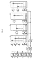
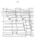
- FIG. 1 A simplified block diagram of a memory with Column redundancy, according to the prior art, is in Figure 1 shown.
- the coding units are for the redundant ones Columns assigned non-blocking.
- Figure 1 shows one Control unit CTRL which controls the external control clock RAS (Row-Address-Strobe), CAS (Column-Address-Strobe), WE (Write Enable) and possibly OE (Output Enable) processed.
- RAS Row-Address-Strobe
- CAS Columnumn-Address-Strobe
- WE Write Enable
- OE Output Enable
- a row address buffer unit is RABF shown, which from the external addresses EXAO ... q internal Row addresses RAB under the control of control lines derived from the unit CTRL.
- one Column address buffer unit CABF represented that the external addresses EXAO ... q together with control lines internal column addresses from the control unit CTRL CAB generated.
- An input-output unit IOB is provided those for data transfer to and from memory worries.
- External data lines EXDO ... p are connected to it.
- a memory block BK n consists of a cell array with a known matrix-type arrangement of memory cells, word lines WL 1, n ... WL x, n and bit line pairs BLG 1, n ... BLG y, n , where, for example, a "folded bitline" Arrangement BL, / BL is shown, from a block decoder BKDEC and a word decoder / driver RDEC 1 ... n , further from bit amplifiers / switches BS 1, n BS y, n and finally from data bit amplifiers / switches DSW 1 ... n (1 ⁇ n ⁇ N).
- a single memory block is activated by its associated block decoder BKDEC n .
- a first part of the row addresses RAB is supplied to the block decoders BKDEC n .
- These addresses are so numerous that a 1 out of N selection can be made.
- the block selection line BKS n of a selected block decoder BKDEC n activates the associated word decoder / driver RDEC n and the data bit amplifier / switch DSW n .
- the word lines of a memory block BK n are selected by the active word decoder / driver RDEC n , to which the second part of the row addresses is supplied for this purpose. Redundant word lines are not shown here.
- the signals of the bit line pairs BLG y, n are amplified by the activated bit amplifier DSW n and switched in groups by means of bit switches BS y, n to the block data bus BKDB n of the corresponding width. These bit switches are each operated by an active bit group selection line CSL 1 ... Y from the common column decoder CDEC.
- the column decoder CDEC also has a control input CFR. If this signal is inactive, ie if it is, for example, logic "0" with positive logic, all selection lines are deactivated.
- the data on the block data bus BKDB n are amplified during a read cycle and switched to the input-output bus IOBS via the data bit switches from DSW n .
- This bus 10BS connects the data bit switch DSW n to the input-output buffer 10B.
- the data from the input-output bus are written IOBS this switch on the Block Scheme BKDB n and the selected bit switches BS y, n stored in the respective cells in a write cycle.
- two redundant bit line groups RBLG 1.1 ... 2.2 with their associated bit amplifiers / switches RBS 1.1 ... 2.2 are also shown. These bit switch groups are each activated by a redundant selection line RCSL 1 or RCSL 2 from the redundant drivers RCD 1 or RCD 2 common to all memory blocks BK n .
- the function of a redundant unit is identical to that of a normal unit.
- FIG. 1 also shows two groups of N coding elements CF 1 ... N, 1 ... 2 each, ie one element per memory block BK nT and per redundant selection line RCSL 1 or RCSL 2 .
- These coding elements CF n, 1 ... 2 receive as input the first part of the row addresses RAB, which is responsible for block decoding 1 from N, and the same column addresses CAB as the column decoder CDEC. Their outputs are connected on two separate lines; CF 1 ... N, 1 on RD 1 or CF 1 ... N, 2 on RD 2 . These lines are fed to the inputs of the redundant drivers RCD 1 or RCD 2 and a NOR gate. The output of the NOR gate forms the input CFR of the column decoder.
- a memory block BK n is activated by the corresponding block decoder BKDEC n.
- the two associated coding elements CF n, 1 and CF n, 2 are also selected with the same row-address combination.
- the lines RD 1 and RD 2 are normally inactive, for example logical "0". Accordingly, the redundant failure lines RCSL 1 and RCSL 2 are also inactive, and the control signal CFR, here logical "1", enables the column decoder CDEC.
- a failure line CSLi corresponding to the column addresses CAB is therefore selected and switches a normal bit line group BLG y, n on the block data bus BKDB n of the active memory block BK n .
- the faulty units are marked with the letters AG.
- In the first block three errors occur A, B, C, in the second and third errors D and E respectively and in the last block two F and G.
- On the left side of FIG. 2 is the utilization of the coding elements CF1,1. .CF4.2 shown. Since only two defective units can be repaired per memory block BK1 ... 4, it is clear that in this example the memory cannot be repaired, although two unused decoding elements remain, since only six of the eight coding elements CF 1, CF 1, 1 ... 4.2 can be used. Faulty places in the memory blocks BK1 ... 4 are marked with a cross. The defective units replaced by redundant bit line groups are marked with a circle.
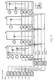
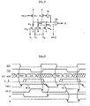
- FIG. 3 shows a conventional circuit according to the prior art for coding the column addresses in the case of non-blocking column redundancy in the event that laser-separable fuse blocks are used as coding elements in the circuit arrangement according to FIG.
- the two groups of coding elements mentioned above have an identical structure and are represented as units E 1 and E 2 , only one being shown in detail.
- Such a unit E 1 consists of N identical circuits CF 1 ... N, 1 for E 1 or CF 1 ... N, 2 for E 2 and a NAND gate NGN with N inputs RDN 1 ... N and an output RD 1 at E 1 or RD 2 at E 2 .
- the two output signals RD 1 and RD 2 are each fed to a redundant driver RCD 1 or RCD 2 with the outputs RCSL 1 or RCSL 2 and the gate NOR already shown in FIG.
- the output of this gate NOR is connected to a driver CFRD, the output of which is the signal CFR.
- These three drivers consist of a NAND gate and a downstream inverter.
- the second input of these NAND gates is connected to an enable signal FR which, in the case of a logic "0" state, keeps both the normal and the redundant selection lines at logic "0" at a low potential. This release signal FR is usually used for synchronization purposes.
- Such a circuit CF i, j consists of a NAND gate NGN with M inputs, a downstream inverter P1, N1, and 2 x K N-channel transistors in series, each with a fuse element, which are connected to the output A of the inverter P1, N1 connected in parallel and from an output inverter IV.
- the block selection takes place via the input NAND gate NGN, which, for example, is one of all possible combinations of M lines from the M block address lines X 1 ... M and their complementary lines / X 1 ... M is supplied.
- a circuit CF i, j is activated when all inputs of this NAND gate are logic "1".
- EP 0 492 099 also represents such a circuit.
- a disadvantage of the solution described is that when a non-programmed column address is created, ie in Y-1 cases of Y, a cross current flows across the transistor P1 of the selected circuit CF i, j after the low potential in the entire active cycle. This cross current may occur twice in each memory block group E 1 , E 2 and takes on an impermissibly high value in the case of concrete solutions with several such groups.
- Another disadvantage is, also in specific cases, the excessive number of lines RDN 1 ... N and the resulting disadvantageously large output gate NGN.
- the object of the present invention is an improved Utilization of the existing fuselocks in the enlargement of column redundancy and a reduction in To allow electricity consumption.
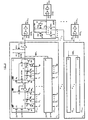
- FIG. 4 shows, as an example of an implementation of the block-free column redundancy according to the invention, the simplified block diagram of a memory with the same basic organization as in FIG. 1.
- each memory block BK N contains, for example, twice the number of redundant bit line groups RBL-G 1, n .. .4, n and bit amplifiers / switches RBS 1, n ... 4, n .
- the four redundant selection lines RCSL 1 ... 4 are operated by four redundant drivers RCD 1 ... 4 common to all memory blocks.
- a memory block BK n is activated with a specific row-address combination.
- Lines RD 1 ... 4 are normally inactive and, accordingly, the redundant failure lines RCSL 1 ... 4 .
- the control signal CFR is therefore logic "1" and activates the column decoder CDEC. If a addressed memory cell of the bit line group BLGy, n is defective in the memory block BK n , a coding element CF i, j is programmed for the corresponding block and column addresses. When this block address occurs, the coding element CF i, j programmed for this is selected and the line RD j is activated when the corresponding column address is created.
- the thereby inactive control signal CFR blocks the column decoder CDEC and the redundant line RCSL j is operated instead of the selection line CSL y .
- the total number of possible repairs remains 2 x N as in the first solution.
- this new solution up to four such elements CF i, 1 ... 4 are available for repair purposes per memory block.
- the space requirement for the redundant bit line groups BLG y, n is the same as when the column redundancy of the first solution is doubled.
- the number of memory blocks BK n is generally much smaller than the number of selection lines CSL y , only a few additional addresses need to be programmable for the modified coding elements CF i, j .
- FIG. 5 shows a repair example with block-free column redundancy for the same arrangement as in FIG. 2. In this case, the memory can obviously be repaired.
- the same elements in FIG. 2 and FIG. 5 have the same designation. 5, in contrast to FIG. 2, block-independent coding elements CF 1.1 ... CF 2.4 and here four redundant drivers RCD 1 ... RCD 4 are provided, in contrast to FIG. Defective storage cells are again symbolically marked with a cross and those that have been repaired are outlined with a circle.
- FIG. 1 and FIG. 4 each show a redundancy arrangement in which n coding elements CF i, j can be assigned to each active memory block BK.
- the same block address bus CAB, RAB, CTB, which is responsible for the memory block decoding, is fed to these coding elements CF i, j .
- the coding elements CF i, j are assigned to a plurality of memory blocks simultaneously. Only a subset of the block addresses is then supplied to these coding elements. A defective bit line group is replaced in all of these memory blocks simultaneously and regardless of the memory block in which a defect is actually located.
- a memory block BK n can be understood as a group of Q individual memory blocks BK n, 1... Q in the sense of the invention without any restriction.
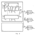
- FIG. 6 shows a circuit according to the invention for coding the column addresses in the case of block-free column redundancy with fuse blocks as coding elements.
- the input of the inverter IE is a line RDNj common to all P circuits.
- the transistors PE1 and PE2 are connected between the high potential (VDD) and this line.
- the structure and function of these drivers are the same as in FIG. 3.
- the circuit DNOR consists of two P-channel transistors PD1 and PD2 connected in parallel between the high potential VDD and a node D, and four N-channel transistors ND 1..4 connected in parallel between the node D and the low potential VSS. and from an inverter ID with input signal D.
- the gate of PD1 is connected to the signal ATDN.
- the output of ID is connected to the gate of PD2 in a retention configuration.
- the gates of the transistors ND 1..4 are connected to the lines RD 1..4 .
- Such a circuit consists of two P-channel transistors P1 and P2 connected in series, and of an N-channel transistor N1.
- the enable signal EN is connected to the gates of P1 and N1 and the set signal SP is connected to the gate of P2.
- the common connection A between P2 and N1 is the input of an inverter IV with a P-channel transistor P3 in a retention configuration.
- 2xM N-channel transistors TX 1 ... M , TNX 1 ... M are also connected in series with one fuse element FX 1 ...
- the gates of these transistors are connected to the row addresses X 1..M and / X 1..M .
- the output B of the inverter IV is connected to the gates of the P-channel transistor P4 and the N-channel transistor N2.
- a further P-channel transistor P5 with a gate signal ATDN is located between these transistors.
- the common terminal C between N2 and P5 is the input of a pull-down N-channel transistor N3, the drain output of which is connected to the common line RDN j .
- a last P-channel transistor P6 is connected at the common connection between P4 and P5 and at connection C. Its gate is connected to the output line RDN j in a restraint configuration.
- 2xK N-channel transistors TY 1 ... K , TNY 1 ... K are connected in series with a fuse element FY 1 ... K , FNY 1 ... K in parallel at connection C.
- the gates of these transistors are connected to the column addresses Y 1..K and / Y 1..K .
- the function of the circuit described is based on the Time diagram of Figure 7 explained, only the necessary Memory signals are shown.
- the first part shows a cycle without using column redundancy while the second part represents the activation of this redundancy.
- a write or read cycle is initiated by the falling edge of the / RAS signal, the externally applied row addresses being saved. Shortly afterwards, a certain combination of M lines from the 2xM block address lines X i and / X i is actively log. "1".
- the enable signal EN which is also used elsewhere on the memory, is logged. "0".
- the transistor P1 becomes conductive.
- the transistor N1 is blocked. With a small delay T1 after all active block address lines have assumed a stable logic state, the set signal SP becomes log for the duration T2 (a few nanoseconds). "0". During this time T2, both transistors P1 and P2 are conductive.
- This current which occurs with completely fault-free memories in all circuits CF i, j , can, however, be kept extremely small by dimensioning the transistors P1 and P2 and by a minimal time period T2.
- the fact that a relatively long period of time for the block decoding of the column redundancy is available for DRAM memories is exploited here in particular.
- the input part of the circuit CF i, j which is responsible for this block decoding, therefore does not have to have a high speed.
- the first write or read cycle of FIG. 7 is ended by the rising / RAS edge, which resets the signal EN at high potential and the signal FR at low potential.
- all circuits CF i, j and the redundant selection lines RCSL 1..4 are inactive by EN or FR.
- the bit decoder is log with CFR. "0" locked.
- a redundancy case is shown in the second part of the time diagram in FIG.
- the beginning of a write or read cycle is like the first part. If for a circuit CF i, j in any unit E j all fuse elements are separated in which the associated block addresses have the value log. Assuming "1", node A rises to high potential because of the switched-on P-channel transistors P1 and P2.
- the output B of the inverter IV is log. "0" and turns on the retention transistor P3.
- the state log. "1" of A is therefore retained after T2 (SP again log. "1").
- the circuit CF i, j is selected. Of course, only one such circuit may be active in each unit E j .
- the transistors P4 and P5 are switched on by B and ATDN (both log. "0"), the transistor N2, however, is switched off. As a result, a charging current can flow from the high potential VDD to the node C. If for this circuit CF i, j all fuse elements are separated in which the associated column addresses log. Are "1", node C rises to high potential. This turns on the N-channel transistor N3.
- This transistor is dimensioned such that the line RDN j of the relevant unit E j is discharged to a low potential near VSS, although the P-channel transistors PE1 and PE2 are initially still conductive. With a low potential on this line, the transistor P6 of the circuit CF i, j is switched on and the output of the inverter IE in the state log. "1" switched. The retention transistor PE2 does not become conductive as a result. The potential of RDN j can decrease further. With a certain delay after the column addresses have become stable or after the enable signal FR has risen to high potential, the control signal ATDN becomes log. "1". Now the transistor PE1 is also switched off and the line RDN j drops to the low potential VSS (log. "0"). Although P5 is now also switched off, node C remains log through the switched on transistors P4 and P6. "1". In contrast to the solution from FIG. 5, no cross current flows in the circuit CF i, j in this state.
- the main advantage of the solution shown in FIG. 4 and FIG. 6 is the better utilization of the coding elements with a small space requirement.
- An advantage of the circuit shown in FIG. 6 is the reduction in power consumption by approximately 70% compared to a conventional solution by using the clock ATDN. The generation of this signal, which is coupled to the enable signal FR and plays a role in the so-called "fast page mode" when changing the column addresses, is not discussed in detail, however, because this is not part of the invention.
- Another advantage of this circuit in concrete implementations is the use of only one line RDN j with pull-down transistors N3 in the units E j .
- a variant of the block coding is shown for the circuit CF in FIG.
- This coding circuit has the advantage that no cross current flows during the selection. An additional NAND gate is required for this.
- the circuit consists of two P-channel transistors P1 and P2, an inverter IN, a NAND gate NG and the same N-channel transistors TX 1 ... TX M with fuse elements TX 1 ... FNX M as in Figure 6.
- the transistors P1 and P2 are connected between the high potential VDD and the node A.
- the signal PRCH and the output of the inverter IN are carried at the gate of P1 and P2, respectively.
- the input from the inverter IN, a first input of the NAND gate NG and the coding elements connected in parallel are connected to the node A.
- the XVLD signal is carried at the second input of NG, the output of which is the aforementioned signal B.
- FIG. 9 shows a time diagram of the signals used to explain the function of this circuit.
- the signals PRCH, XVLD and the block addresses X i , / X i , i 1..M log. "0".
- all N-channel transistors are blocked and the P-channel transistor P1 is conductive.
- the node A is therefore log. "1” and the inverter output log. "0".
- the transistor P2 is also conductive.
- the output B of the NAND gate NG is log. “1” because XVLD log the status. Shows "0". As already explained, this deactivates the column coding part.
- the state log. "1" of node A remains due to the transistor being switched on P2 received.
- the node A remains log. "1” in the case of a Block selection because the fuse elements with block addresses in the State log. "1" are separated. Otherwise he will discharged through a conductive connection to VSS and the Inverter turns off P-channel transistor P2.
- T1 time after the block addresses become stable the level of the XVLD signal increases. Thereby the output B log. "0" and the subsequent circuit is switched on as in FIG. 6. If the block addresses present are not programmed the signal B remains log. "1".
- XVLD falls with the rising / RAS edge to low potential.
- Signal B becomes log. "1” and the column coding of the circuit CF is turned off.
- the block addresses are then followed by the signal PRCH, reset (log. "0"). This causes node A to rise back to high potential.
- Advantage of the circuit is that no cross current flows through transistor Pl, if the pending block addresses have not been programmed are.
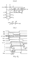
- FIG. 10 shows a circuit for generating the set pulse SP from FIG. 6 and an additional circuit for forming the signal XVLD from FIG. 8.
- the first circuit consists of two P-channel transistors P1 and P2, an inverter I1 and an inverting one Delay element VG, from a NAND gate NG1 and in this example from three pairs of N-channel transistors 1 ... 6.
- Transistors P1 and P2 are connected in parallel between VDD and node A.
- the PRCH signal is connected to the gate of P1.
- the node A is the input of the inverter I1.
- the output B of this inverter I1 is connected to the gate of P2, to a first input of the NAND gate NG1 and to the input of the delay element VG.
- the output C of this element is the second input of NG1 with the output signal SP.
- the delay element VG consists of an odd number of inverters I2, I3, I4 connected in series with delay capacitors C1, C2 in a known manner. In this example three inverters and two capacitors are shown.
- NG1 and VG In the circuit for generating XVLD become NG1 and VG by a NAND gate NG2 and one downstream inverter 15 replaced with output signal XVLD.
- the inputs of NG2 are the signals RINT and B.
- the RINT signal which is otherwise used in the memory, is a clock inverted with respect to the external / RAS signal.
- the N-channel transistors between node A and VSS are all blocked in this state, but P1 is conductive. This means that A is high and B is low.
- the transistor P2 is switched on.
- With the signal B in the state log. "0" are the outputs SP and C of NG1 and VG log. "1”.
- the XVLD signal is log. "0". With the falling / RAS edge, PRCH rises to high potential.
- the RINT, X i , / X i and PRCH signals are logged successively with the rising / RAS edge. "0".
- the output C of VG is logged with a delay. "1”. Since after the setting pulse SP either C or B log. Are “0", SP log also remains. "1".
Abstract
Description
Die Erfindung betrifft eine Spalten-Redundanz-Schaltungsanordnung
für einen Speicher gemäß dem Oberbegriff des Anspruchs
1.The invention relates to a column redundancy circuit arrangement
for a memory according to the preamble of the
Eine derartige Anordnung ist z.B. aus IEEE Journal of Solid State Circuits, Vol. 26, No. 1, Januar 1991 auf Seite 12ff beschrieben. Auch EP-A-0 472 209 stellt eine derartige Anordnung dar.Such an arrangement is e.g. from IEEE Journal of Solid State Circuits, Vol. 26, No. January 1, 1991 Page 12ff. EP-A-0 472 209 also represents such an arrangement.
Die Verkleinerung der Rastermaße bei jeder neuen Speichergeneration erhöht die Anfälligkeit für Defekte im Zellenfeld. Eine rentable Produktion erfordert daher Vorrichtungen auf dem Speicher, mit denen solche Defekte repariert werden können. In der Regel sind Zusatz-Zellen vorgesehen, die mittels programmierbarer Codierungselemente anstelle der defekten Zellen eingesetzt werden.The reduction of the grid dimensions with every new storage generation increases the susceptibility to defects in the cell field. Profitable production therefore requires devices on the memory with which such defects are repaired can be. As a rule, additional cells are provided, using programmable coding elements instead the defective cells are used.
Bei Speichern größerer Kapazität sind die Speicherzellen in mehrere Blöcke unterteilt. Wegen der matrixförmigen Anordnung der Speicherzellen, müssen die Zusatz-Zellen ebenfalls in Zeilen und Spalten angeordnet werden. Diese redundanten Leitungen sind im allgemeinen am Rande der Zellenfelder ausgebildet. Sie werden jeweils durch ein programmierbares Element im Zusammenhang mit den angelegten Adressen selektiert.When storing larger capacity, the memory cells divided into several blocks. Because of the matrix-like arrangement of the memory cells, the additional cells must also arranged in rows and columns. This redundant Lines are generally on the edge of the cell fields educated. They are each programmable Element related to the created Addresses selected.
Diese programmierbaren Elemente können z.B. lasertrennbare Fuseblöcke sein. Üblicherweise wird jeder Fuseblock einer oder mehreren redundanten Leitungen fest zugeordnet. Soll die Reparaturfähigkeit gesteigert werden, muß die Anzahl der redundanten Leitungen erhöht und damit auch die Anzahl der Fuseblöcke vergrößert werden. Der Platzbedarf einer solchen Redundanz-Vergrößerung ist wesentlich und kann zu einer Verringerung der Stückzahl pro Scheibe führen. Bei den derzeitigen Speichergenerationen ist die benötigte Fläche für die Fuseblöcke zusammen mit deren Ansteuerschaltungen in etwa so groß wie die Fläche, welche die redundanten Speicherzellen in Anspruch nehmen. Einerseits zeigt eine Statistik der Redundanz-Ausnutzung, z.B. bei einem 4-Mega-Speicher, daß im Mittel nur die Hälfte der Fuseblöcke zur Reparatur eingesetzt werden. Andererseits hat sich bei der Defektanalyse herausgestellt, daß eine Verdoppelung der Redundanz bis zu 20 % mehr Ausbeute ermöglicht. Dies zeigt, daß bei der bisherigen Auslegung der Redundanzarchitektur, ein wesentlicher Anteil von Speichern nicht repariert werden kann, obwohl im Prinzip genügend programmierbare Codierungselemente zur Verfügung stehen.These programmable elements can e.g. laser separable Be fuselocks. Usually every fuseblock becomes one or several redundant lines. Should the number of repairs must be increased of the redundant lines and thus also the number the fuselocks are enlarged. The space requirement of one such redundancy increase is essential and can lead to a reduction in the number of pieces per disc. At the current memory generations is the one needed Area for the fuse blocks together with their control circuits about the size of the area that the use redundant memory cells. On the one hand shows a statistic of the redundancy utilization, e.g. at a 4 mega memory that on average only half of the Fuse blocks can be used for repair. On the other hand has found in the defect analysis that a Doubling the redundancy allows up to 20% more yield. This shows that the previous interpretation of the Redundancy architecture, an essential part of storage cannot be repaired, although in principle enough programmable coding elements are available.
Soll die Reparaturfähigkeit erhöht werden, so wäre es aus Platzgründen von Vorteil, wenn nur die Anzahl der redundanten Leitungen vergrößert werden müßte und mittels geeigneter Schaltung eine bessere Ausnutzung der vorhandenen Fuseblöcke erreicht werden könnte.If the ability to repair should be increased, it would be over Space is an advantage if only the number of redundant ones Lines would have to be enlarged and by means of suitable Circuit to better utilize the existing Fuse blocks could be achieved.
Bei einer Erweiterung der Spaltenredundanz stellt der Anstieg des Stromverbrauchs ein weiteres Problem dar. Im Gegensatz zur Ansteuerung der Reihenredundanz, die nur am Anfang eines Zyklus eingesetzt wird, muß die Ansteuerung der Spaltenredundanz im gesamten aktiven Zyklus betriebsbereit sein. Da für diese Ansteuerung bisher Schaltungen mit dynamischer Logik und Querstromanteilen verwendet worden sind, bedeutet die Erweiterung der Spaltenredundanz gleichzeitig auch einen Anstieg des Stromverbrauchs. If the column redundancy is expanded, the increase of electricity consumption is another problem. In contrast to control the row redundancy, which is only on Control must be used at the beginning of a cycle the column redundancy is ready for operation in the entire active cycle his. As circuits for this control so far with dynamic logic and cross current components means expanding column redundancy at the same time an increase in electricity consumption.
Ein vereinfachtes Blockschaltbild eines Speichers mit Spaltenredundanz, gemäß dem Stand der Technik ist in Figur 1 dargestellt. Dabei sind die Codiereinheiten für die redundanten Spalten blockfest zugeordnet. Figur 1 zeigt eine Kontrolleinheit CTRL, die die externen anliegenden Steuertakte RAS (Row-Address-Strobe),CAS (Column-Address-Strobe), WE (Write Enable) und gegebenenfalls OE (Output Enable) verarbeitet. In dieser Kontrolleinheit CTRL werden die üblichen internen Steuertakte erzeugt, die auf der Abbildung schematisch in einem Steuerbus CTB zusammengefaßt sind. Weiterhin ist eine Reihen-Adreß-Buffer-Einheit RABF dargestellt, die aus den externen Adressen EXAO...q interne Reihen-Adressen RAB unter der Kontrolle von Steuerleitungen aus der Einheit CTRL ableitet. Weiterhin ist eine Spalten-Adreß-Buffer-Einheit CABF dargestellt, die aus den externen Adressen EXAO...q zusammen mit Steuerleitungen aus der Kontrolleinheit CTRL interne Spaltenadressen CAB generiert. Eine Input-Output-Einheit IOB ist vorgesehen, die für den Datentransfer in und aus dem Speicher sorgt. An ihr sind externe Datenleitungen EXDO...p angeschlossen.A simplified block diagram of a memory with Column redundancy, according to the prior art, is in Figure 1 shown. The coding units are for the redundant ones Columns assigned non-blocking. Figure 1 shows one Control unit CTRL which controls the external control clock RAS (Row-Address-Strobe), CAS (Column-Address-Strobe), WE (Write Enable) and possibly OE (Output Enable) processed. In this control unit become CTRL generates the usual internal control clocks that are on the picture schematically summarized in a control bus CTB are. Furthermore, a row address buffer unit is RABF shown, which from the external addresses EXAO ... q internal Row addresses RAB under the control of control lines derived from the unit CTRL. Furthermore, one Column address buffer unit CABF represented that the external addresses EXAO ... q together with control lines internal column addresses from the control unit CTRL CAB generated. An input-output unit IOB is provided those for data transfer to and from memory worries. External data lines EXDO ... p are connected to it.
Diese Einheiten bilden die Standard-Peripherie des Speichers und werden deswegen nicht näher beschrieben. Die Funktion verschiedener Steuerleitungen wird nur in späteren Abschnitten erläutert, bei denen dies zum Verständnis einzelner Schaltungen notwendig ist.These units form the standard periphery of the memory and are therefore not described in more detail. The Function of different control lines is only in later Sections explained where this is for understanding individual circuits is necessary.
Ferner sind in Figur 1 eine Gruppe von N Speicherblöcken BK1...N gezeigt, wobei N ein Vielfaches von 2 ist, z.B. N=2m, und von denen zwei, BK1 und BKn in Figur 1 dargestellt sind. Weiterhin ist ein für alle Blöcke BKn (n=1...N) gemeinsamer Spaltendekoder CDEC dargestellt und, ohne allgemeine Beschränkung, zwei für alle Blöcke BK1...N gemeinsame redundante Spaltendekoder RCD1 und RCD2. Schließlich sind zwei Gruppen von je N Codierungselementen CF1...N,1...2 für die Adreßcodierung und Spaltenredundanz, die später beschrieben werden, dargestellt.1 shows a group of N memory blocks BK 1... N , where N is a multiple of 2, for example N = 2 m , and two of which, BK 1 and BK n, are shown in FIG. Furthermore, a column decoder CDEC common for all blocks BK n (n = 1 ... N) is shown and, without general restriction, two redundant column decoders RCD 1 and RCD 2 common for all blocks BK 1 ... N. Finally, two groups of N coding elements CF 1 ... N, 1 ... 2 each for address coding and column redundancy, which will be described later, are shown.
Die Verwendung von gemeinsamen Spaltendekodern CDEC ist bei Speichern höherer Kapazität aus Platzgründen geläufig. Bis auf die vier ersten Peripherie-Einheiten, die nur einmal auf dem Speicher vorkommen, können selbstverständlich die restlichen Bestandteile mehrmals parallel aufgebaut werden. Figur 1 zeigt nur aus Gründen der Übersichtlichkeit eine einzige Gruppe von Speicherblöcken BK1...N.The use of common column decoders CDEC is common when storing larger capacities for reasons of space. Except for the first four peripheral units, which only appear once on the memory, the remaining components can of course be set up several times in parallel. Figure 1 shows a single group of memory blocks BK 1 ... N only for reasons of clarity.
Ein Speicherblock BKn besteht aus einem Zellenfeld mit bekannter matrixförmiger Anordnung von Speicherzellen, Wortleitungen WL1,n...WLx,n und Bitleitungspaaren BLG1,n...BLGy,n, wobei hier z.B.eine "Folded-Bitlines"-Anordnung BL,/BL gezeigt ist, aus einem Blockdekoder BKDEC und einem Wort-Dekoder/Treiber RDEC1...n, ferner aus Bit-Verstärkern/Schaltern BS1,nBSy,n und schließlich aus Datenbit-Verstärkern/Schaltern DSW1...n (1≤n≤N).A memory block BK n consists of a cell array with a known matrix-type arrangement of memory cells, word lines WL 1, n ... WL x, n and bit line pairs BLG 1, n ... BLG y, n , where, for example, a "folded bitline" Arrangement BL, / BL is shown, from a block decoder BKDEC and a word decoder / driver RDEC 1 ... n , further from bit amplifiers / switches BS 1, n BS y, n and finally from data bit amplifiers / switches DSW 1 ... n (1≤n≤N).
Bei der gezeigten Darstellung ist jeweils nur ein einziger Speicherblock durch seinen zugehörigen Blockdekoder BKDECn aktiviert. Zu diesem Zweck wird ein erster Teil der Reihenadressen RAB den Blockdekodern BKDECn zugeführt. Diese Adressen sind so zahlreich, daß eine 1 aus N Auswahl getroffen werden kann. Die Blockauswahlleitung BKSn eines selektierten Blockdekoders BKDECn aktiviert den zugehörigen Wort-Dekoder/Treiber RDECn und die Datenbit-Verstärker/Schalter DSWn. Die Wortleitungen eines Speicherblocks BKn werden durch den aktiven Wort-Dekoder/Treiber RDECn selektiert, dem zu diesem Zweck der zweite Teil der Reihenadressen zugeführt wird. Redundante Wortleitungen sind hier nicht gezeigt.In the illustration shown, only a single memory block is activated by its associated block decoder BKDEC n . For this purpose, a first part of the row addresses RAB is supplied to the block decoders BKDEC n . These addresses are so numerous that a 1 out of N selection can be made. The block selection line BKS n of a selected block decoder BKDEC n activates the associated word decoder / driver RDEC n and the data bit amplifier / switch DSW n . The word lines of a memory block BK n are selected by the active word decoder / driver RDEC n , to which the second part of the row addresses is supplied for this purpose. Redundant word lines are not shown here.
Die Signale der Bitleitungspaare BLGy,n werden durch den aktivierten Bit-Verstärker DSWn verstärkt und gruppenweise mittels Bitschaltern BSy,n auf den Blockdatenbus BKDBn der entsprechenden Breite geschaltet. Diese Bit-Schalter werden jeweils durch eine aktive Bitgruppen-Auswahl-Leitung CSL1...Y aus dem gemeinsamen Spaltendekoder CDEC betrieben. Die Bitgruppenauswahlleitungen CSL1...Y werden durch den Spaltendekoder CDEC selektiert, dem hierfür ein erster Teil der Spalten-Adressen zugeführt wird. Der andere Teil dieser Adressen wird für die Daten-Dekodierung bei dem Input-Output-Buffer 10B verwendet. Bei dem in Figur 1 gezeigten Beispiel sind Y Bitgruppen-Auswahl-Leitungen vorhanden, wobei 2k=Y gilt. Es sind also K Spaltenadressen zur Dekodierung der Y Auswahl-Leitungen vorhanden. Die Auswahl-Leitungen haben nur in dem aktiven Block eine Wirkung. Der Spaltendekoder CDEC besitzt zusätzlich einen Steuereingang CFR. Wenn dieses Signal inaktiv ist, d.h. wenn es z.B. logisch "0" bei positiver Logik ist, werden sämtliche Auswahl-Leitungen deaktiviert.The signals of the bit line pairs BLG y, n are amplified by the activated bit amplifier DSW n and switched in groups by means of bit switches BS y, n to the block data bus BKDB n of the corresponding width. These bit switches are each operated by an active bit group selection line CSL 1 ... Y from the common column decoder CDEC. The bit group selection lines CSL 1 ... Y are selected by the column decoder CDEC, to which a first part of the column addresses is supplied. The other part of these addresses is used for data decoding in the input-output buffer 10B. In the example shown in FIG. 1, there are Y bit group selection lines, where 2 k = Y applies. There are therefore K column addresses for decoding the Y selection lines. The selection lines only have an effect in the active block. The column decoder CDEC also has a control input CFR. If this signal is inactive, ie if it is, for example, logic "0" with positive logic, all selection lines are deactivated.
Die Daten auf dem Blockdatenbus BKDBn werden bei einem Lesezyklus verstärkt und über die Datenbit-Schalter von DSWn auf den Input-Output-Bus IOBS geschaltet. Dieser Bus 10BS verbindet die Datenbit-Schalter DSWn mit dem Input-Output-Buffer 10B. Umgekehrt werden bei einem Schreib-Zyklus die Daten von dem Input-Output-Bus IOBS über diese Schalter auf dem Blockdatenbus BKDBn geschrieben und über die selektierten Bitschalter BSy,n in den jeweiligen Zellen gespeichert. The data on the block data bus BKDB n are amplified during a read cycle and switched to the input-output bus IOBS via the data bit switches from DSW n . This bus 10BS connects the data bit switch DSW n to the input-output buffer 10B. Conversely, the data from the input-output bus are written IOBS this switch on the Blockdatenbus BKDB n and the selected bit switches BS y, n stored in the respective cells in a write cycle.
Bei jeden Speicherblock der Figur 1 sind zusätzlich zwei redundante Bitleitungsgruppen RBLG1,1...2,2 mit ihren zugehörigen Bit-Verstärkern/Schaltern RBS1,1...2,2 gezeigt. Diese Bitschalter-Gruppen werden jeweils durch eine redundante Auswahlleitung RCSL1 bzw. RCSL2 aus den für alle Speicherblöcke BKn gemeinsamen redundanten Treibern RCD1 bzw. RCD2 aktiviert. Die Funktion einer redundanten Einheit ist identisch mit der einer normalen Einheit.For each memory block in FIG. 1, two redundant bit line groups RBLG 1.1 ... 2.2 with their associated bit amplifiers / switches RBS 1.1 ... 2.2 are also shown. These bit switch groups are each activated by a redundant selection line RCSL 1 or RCSL 2 from the redundant drivers RCD 1 or RCD 2 common to all memory blocks BK n . The function of a redundant unit is identical to that of a normal unit.
Schließlich sind in der Figur 1 noch zwei Gruppen von je N
Codierungselementen CF1...N,1...2 dargestellt, d.h. ein
Element pro Speicherblock BKnT und pro redundanter Auswahlleitung
RCSL1 bzw. RCSL2. Diese Codierungselemente
CFn,1...2 erhalten als Eingang den ersten Teil der Reihen-adressen
RAB, der für die Blockdekodierung 1 aus N zuständig
ist und dieselben Spaltenadressen CAB wie der Spalten-dekoder
CDEC. Ihre Ausgänge sind auf zwei getrennten Leitungen
geschaltet; CF1...N,1 auf RD1 bzw. CF1...N,2 auf
RD2. Diese Leitungen sind den Eingängen der redundanten
Treiber RCD1 bzw. RCD2 und einem NOR-Gatter zugeführt. Der
Ausgang des NOR-Gatters bildet den Eingang CFR des Spaltendekoders.Finally, FIG. 1 also shows two groups of N coding elements CF 1 ... N, 1 ... 2 each, ie one element per memory block BK nT and per redundant selection line RCSL 1 or RCSL 2 . These coding elements CF n, 1 ... 2 receive as input the first part of the row addresses RAB, which is responsible for
Bei jeden Zyklus wird ein Speicherblock, BKn über den entsprechenden Blockdekoder BKDECn aktiviert. Mit derselben Reihen-Adreß-Kombination werden auch die zwei zugehörigen Codierungselemente CFn,1 und CFn,2 selektiert. Im Normalfall sind die Leitungen RD1 und RD2 inaktiv z.B. logische "0". Dementsprechend sind auch die redundanten Ausfall-Leitungen RCSL1 und RCSL2 inaktiv, und das Steuersignal CFR, hier logisch "1" gibt dem Spaltendekoder CDEC frei. Eine den Spaltenadressen CAB entsprechende Ausfall-Leitung CSLi wird also selektiert und schaltet eine normale Bitleitungsgruppe BLGy,n auf dem Blockdatenbus BKDBn des aktiven Speicherblocks BKn.In each cycle a memory block BK n is activated by the corresponding block decoder BKDEC n. The two associated coding elements CF n, 1 and CF n, 2 are also selected with the same row-address combination. The lines RD 1 and RD 2 are normally inactive, for example logical "0". Accordingly, the redundant failure lines RCSL 1 and RCSL 2 are also inactive, and the control signal CFR, here logical "1", enables the column decoder CDEC. A failure line CSLi corresponding to the column addresses CAB is therefore selected and switches a normal bit line group BLG y, n on the block data bus BKDB n of the active memory block BK n .
Wenn in dem gewählten Speicherblock BKn eine angesprochene Speicherzelle der Bitleitungsgruppe BLGy,n defekt ist, wird eine der zwei Codierungselemente CFn,1 oder CFn,2 für die entsprechende Spaltenadresse programmiert. Beim Auftreten dieser Adresse wird die Leitung RD1 oder RD2 aktiviert. Im hier gezeigten Beispiel sind diese logisch "1". Demzufolge wird das Steuersignal CFR inaktiv, also logische "0", und sperrt den Spaltendekoder CDEC. Die im Normalfall selektierte Auswahlleitung CSLy bleibt dadurch inaktiv stattdessen wird die redundante Leitung RCSL1 oder RCSL2 logisch "1". Dadurch werden die Speicherzellen der Bitleitungsgruppe RBLG1 oder RBLG2 anstelle denen der normalen Einheit angesprochen. Mit der gezeigten Auslegung der Spaltenredundanz können also pro Speicherblock zwei verschiedene Bitleitungsgruppen mit defekten Zellen durch redundante Gruppen ersetzt werden.If a addressed memory cell of the bit line group BLG y, n is defective in the selected memory block BK n , one of the two coding elements CF n, 1 or CF n, 2 is programmed for the corresponding column address. When this address occurs, line RD 1 or RD 2 is activated. In the example shown here, these are logically "1". As a result, the control signal CFR becomes inactive, ie logic "0", and blocks the column decoder CDEC. The selection line CSL y , which is normally selected, thereby remains inactive, instead the redundant line RCSL 1 or RCSL 2 becomes logic "1". As a result, the memory cells of the bit line group RBLG 1 or RBLG 2 are addressed instead of those of the normal unit. With the design of the column redundancy shown, two different bit line groups with defective cells can be replaced by redundant groups per memory block.
Figur 2 zeigt ein Reparaturbeispiel bei blockfester Spaltenredundanz gemäß Figur 1 für den Fall, daß N=4 und zwei redundante Bitleitungsgruppen pro Block vorhanden sind und daß 6 Fehler auftreten. Die fehlerhaften Einheiten sind mit den Buchstaben A-G gekennzeichnet. Im ersten Block treten drei Fehler auf A, B, C , im zweiten und dritten je ein Fehler D bzw. E und im letzten Block zwei F und G. Auf der linken Seite der Figur 2 ist die Ausnutzung der Codierungselemente CF1,1...CF4,2 gezeigt. Da pro Speicherblock BK1...4 nur jeweils zwei fehlerhafte Einheiten repariert werden können, ist klar, daß in diesem Beispiel der Speicher nicht repariert werden kann, obwohl zwei unbenutzte Dekodierungselemente übrig bleiben, da nur sechs der zur Verfügung stehenden acht Codierungselemente CF1,1...4,2 verwendet werden können. Fehlerhafte Stellen in den Speicherblöcken BK1...4 sind mit einem Kreuz gekennzeichnet. Die durch redundante Bitleitungsgruppen ersetzen fehlerhaften Einheiten sind mit einem Kreis gekennzeichnet.FIG. 2 shows a repair example in the case of non-blocking column redundancy according to FIG. 1 for the case that there are N = 4 and two redundant bit line groups per block and that 6 errors occur. The faulty units are marked with the letters AG. In the first block three errors occur A, B, C, in the second and third errors D and E respectively and in the last block two F and G. On the left side of FIG. 2 is the utilization of the coding elements CF1,1. .CF4.2 shown. Since only two defective units can be repaired per memory block BK1 ... 4, it is clear that in this example the memory cannot be repaired, although two unused decoding elements remain, since only six of the eight coding elements CF 1, CF 1, 1 ... 4.2 can be used. Faulty places in the memory blocks BK1 ... 4 are marked with a cross. The defective units replaced by redundant bit line groups are marked with a circle.
Als Codierungselemente werden zumeist sogenannte Fuseblöcke
eingesetzt. Figur 3 zeigt eine übliche Schaltung
gemäß dem Stand der Technik zur Codierung der Spaltenadressen
bei der blockfesten Spalten-Redundanz für den
Fall, daß bei der Schaltungsanordnung gemäß Figur 1 lasertrennbare
Fuseblöcke als Codierungselemente verwendet werden.
Die zwei obengenannten Gruppen von Codierungselementen
sind identisch aufgebaut und als Einheit E1 bzw. E2
dargestellt, wobei nur eine ausführlich gezeigt wird. Eine
solche Einheit E1 besteht aus N identischen Schaltungen
CF1...N,1 bei E1 bzw. CF1...N,2 bei E2 und aus einem NAND-Gatter
NGN mit N Eingängen RDN1...N und einem Ausgang RD1
bei E1 bzw. RD2 bei E2. Die zwei Ausgangssignale RD1 und
RD2 sind je einem redundanten Treiber RCD1 bzw. RCD2 mit
den Ausgängen RCSL1 bzw. RCSL2 und dem in Figur 2 schon
dargestellten Gatter NOR zugeführt. Der Ausgang dieses
Gatters NOR ist an einen Treiber CFRD angeschlossen, dessen
Ausgang das Signal CFR ist. Diese drei Treiber bestehen
aus einem NAND-Gatter und einem nachgeschalteten Inverter.
Der zweite Eingang dieser NAND-Gatter ist an einem
Freigabesignal FR angeschlossen, das bei einem Zustand logisch
"0" sowohl die normalen als auch die redundanten
Auswahlleitungen auf niedrigem Potential logisch "0" hält.
Dieses Freigabesignal FR wird üblicherweise für Synchronisationszwecke
verwendet.
Jede Schaltung CFi,j besitzt ferner M Eingänge für die
Blockcodierung, dabei gilt N=2M, 2 x K Eingänge für die
Spaltenkodierung, dabei gilt Y=2k, und einen Ausgang RDNi,
der mit einem Eingang des NAND-Gatters NGN verbunden ist. So-called fuse blocks are mostly used as coding elements. FIG. 3 shows a conventional circuit according to the prior art for coding the column addresses in the case of non-blocking column redundancy in the event that laser-separable fuse blocks are used as coding elements in the circuit arrangement according to FIG. The two groups of coding elements mentioned above have an identical structure and are represented as units E 1 and E 2 , only one being shown in detail. Such a unit E 1 consists of N identical circuits CF 1 ... N, 1 for E 1 or CF 1 ... N, 2 for E 2 and a NAND gate NGN with N inputs RDN 1 ... N and an output RD 1 at E 1 or RD 2 at E 2 . The two output signals RD 1 and RD 2 are each fed to a redundant driver RCD 1 or RCD 2 with the outputs RCSL 1 or RCSL 2 and the gate NOR already shown in FIG. The output of this gate NOR is connected to a driver CFRD, the output of which is the signal CFR. These three drivers consist of a NAND gate and a downstream inverter. The second input of these NAND gates is connected to an enable signal FR which, in the case of a logic "0" state, keeps both the normal and the redundant selection lines at logic "0" at a low potential. This release signal FR is usually used for synchronization purposes.
Each circuit CF i, j also has M inputs for block coding, where N = 2 M , 2 x K inputs for column coding, Y = 2 k , and an output RDN i , which corresponds to an input of the NAND gate NGN is connected.
Eine solche Schaltung CFi,j besteht aus einem NAND-Gatter NGN mit M Eingängen, aus einem nachgeschalteten Inverter P1, N1, aus 2 x K N-Kanal-Transistoren in Serie mit je einem Fuseelement, die am Ausgang A des Inverters P1, N1 parallel geschaltet und aus einem Ausgangsinverter IV. Die Blockauswahl geschieht über das Eingangs-NAND-Gatter NGN, dem z.B. eine von allen möglichen Kombinationen von M Leitungen aus dem M Block-Adreß-Leitungen X1...M und ihren komplementären Leitungen/X1...M zugeführt wird. Eine Schaltung CFi,j wird dann aktiviert, wenn alle Eingänge dieses NAND-Gatters logisch "1" sind. Sein Ausgang ist dann logisch "0" und der Ausgang A des Inverters P1, N1 demzufolge logisch "Eins". Bei allen anderen Schaltungen CF ist mindestens ein Eingang Xm bzw./Xm logisch "0". Die Inverterausgänge A sind demnach auch logisch "0" und die Leitungen RDNn logisch "1".Such a circuit CF i, j consists of a NAND gate NGN with M inputs, a downstream inverter P1, N1, and 2 x K N-channel transistors in series, each with a fuse element, which are connected to the output A of the inverter P1, N1 connected in parallel and from an output inverter IV. The block selection takes place via the input NAND gate NGN, which, for example, is one of all possible combinations of M lines from the M block address lines X 1 ... M and their complementary lines / X 1 ... M is supplied. A circuit CF i, j is activated when all inputs of this NAND gate are logic "1". Its output is then logic "0" and the output A of the inverter P1, N1 is consequently logic "one". For all other circuits CF, at least one input X m or / X m is logic "0". Accordingly, the inverter outputs A are also logic "0" and the lines RDN n are logic "1".
Wenn Y=2k Auswahlleitungen CSL1...Y vorhanden sind, werden 2 x K Spalten-Adreß-Leitungen für die Codierung einer Spaltenadresse benötigt, ohne allgemeine Beschränkung z.B. Y1...K bzw./Y1...K, weil die Serienschaltung eines n-Kanal-Transistors und eines lasertrennbaren Fuse-Elements nur bei einem Eingangssignal mit Zustand logisch "1" eine Wirkung zeigt.If Y = 2 k selection lines CSL 1 ... Y are available, 2 x K column address lines are required for coding a column address, without general restriction, e.g. Y 1 ... K or / Y 1 ... K , because the series connection of an n-channel transistor and a laser-separable fuse element only has an effect on an input signal with the logic "1" state.
Wenn bei der aktivierten Schaltung CFi,j mindestens ein Fuse-Element, bei dem die entsprechende Spalten-Adreß-Leitung den Zustand logisch "1" hat, nicht getrennt ist, wird der Knoten A über diesen eingeschalteten N-Kanal-Transistor auf so niedrigem Potential gehalten, daß der Ausgangsinverter IV auf logisch "1" schaltet. In diesem Fall haben demnach alle Leitungen RDN1...N den Zustand logisch "1" und die Ausgangsleitung RDJ von NGN den Zustand logisch "0". Die zugeordnete redundante Auswahlleitung RCSLj ist also unabhängig vom Signal FR inaktiv, d.h. logisch "0". Trifft dies für beide Leitungen RD1 und RD2 zu, sind auf beide redundanten Leitungen RCSL1 und RCSL2 inaktiv und der Ausgang des Gatters NOR logisch "1". Wenn das Freigabesignal FR aktiv "1" wird, nimmt das Signal CFR ebenfalls den Zustand logisch "1" an, und entriegelt den Spaltendekoder. In diesem Falle wird eine normale Bitleitungsgruppe selektiert.If, in the activated circuit CF i, j, at least one fuse element, in which the corresponding column address line has the logic "1" state, is not separated, the node A becomes so via this switched-on N-channel transistor kept low potential that the output inverter IV switches to logic "1". In this case, all lines RDN 1 ... N have the state logic "1" and the output line RDJ of NGN the state logic "0". The assigned redundant selection line RCSL j is therefore inactive regardless of the signal FR, ie logically "0". If this applies to both lines RD 1 and RD 2 , both redundant lines RCSL 1 and RCSL 2 are inactive and the output of the gate NOR is logic "1". When the enable signal FR becomes active "1", the signal CFR also assumes the logic "1" state and unlocks the column decoder. In this case, a normal bit line group is selected.
Wenn im Gegenteil bei einer aktiven Schaltung CFi,1 oder CFi,2 alle Fuseelemente getrennt sind, bei denen die entsprechenden Spalten-Adreß-Leitungen logisch "1" sind, bleibt der Knoten A auf hohem Potential geladen und der Ausgangsinverter IV im Zustand logisch "Null". Demzufolge nimmt eine Leitung RD1 oder RD2 den Zustand logisch "1" an. Der Ausgang des Gatters NOR ist also logisch "0". Dies gilt ebenfalls für das Signal CFR unabhängig vom Freigabe-signal FR, so daß der Spaltendekoder verriegelt wird. Dagegen wird die redundante Auswahlleitung RCSL1 oder RCSL2 aktiviert und die entsprechende redundante Bitleitungsgruppe im aktiven Speicherblock BKi selektiert.On the contrary, when an active circuit CF i, 1 or CF i, 2 all fuse elements are separated, in which the corresponding column address lines are logic "1", node A remains charged at high potential and the output inverter IV in the state logical "zero". As a result, a line RD 1 or RD 2 assumes the logic "1" state. The output of the gate NOR is therefore logic "0". This also applies to the CFR signal independently of the release signal FR, so that the column decoder is locked. In contrast, the redundant selection line RCSL 1 or RCSL 2 is activated and the corresponding redundant bit line group is selected in the active memory block BK i .
EP 0 492 099 stellt auch eine solche Schaltung dar.
Ein Nachteil der beschriebenen Lösung ist, daß beim Anlegen einer nichtprogrammierten Spalten-Adresse, d.h. in Y-1 Fällen von Y, im gesamten aktiven Zyklus ein Querstrom über den Transistor P1 der selektierten Schaltung CFi,j nach dem niedrigen Potential fließt. Dieser Querstrom tritt evtl. zweimal bei jeder Speicherblockgruppe E1, E2 auf und nimmt bei konkreten Lösungen mit mehreren solchen Gruppen einen unzulässig hohen Wert an. Ein weiterer Nachteil ist, ebenfalls in konkreten Fällen, die zu hohe Zahl von Leitungen RDN1...N und das dadurch bedingte ungünstig große Ausgangsgatter NGN. A disadvantage of the solution described is that when a non-programmed column address is created, ie in Y-1 cases of Y, a cross current flows across the transistor P1 of the selected circuit CF i, j after the low potential in the entire active cycle. This cross current may occur twice in each memory block group E 1 , E 2 and takes on an impermissibly high value in the case of concrete solutions with several such groups. Another disadvantage is, also in specific cases, the excessive number of lines RDN 1 ... N and the resulting disadvantageously large output gate NGN.
Aufgabe der vorliegenden Erfindung ist es, eine verbesserte Ausnutzung der vorhandenen Fuseblöcke bei der Vergrößerung der Spalten-Redundanz und eine Reduktion des Stromverbrauchs zu ermöglichen.The object of the present invention is an improved Utilization of the existing fuselocks in the enlargement of column redundancy and a reduction in To allow electricity consumption.
Diese Aufgabe wird durch den kennzeichnenden Teil des Anspruchs
1 gelöst. Weiterbildungen sind Kennzeichen der Unteransprüche.This task is accomplished by the characterizing part of the
Die Erfindung wird nachfolgend anhand von 11 Figuren näher erläutert.The invention will now be described with reference to 11 figures explained.
Es zeigen:
Figur 1- ein vereinfachtes Blockschaltbild eines Speichers mit Spalten-Redundanz gemäß dem Stand der Technik,
Figur 2- ein Blockschaltbild, welches ein vereinfachtes Reparaturbeispiel bei blockfester Spaltenredundanz darstellt,
Figur 3- eine Schaltungsanordnung für Fuseblöcke und ihre Ansteuerung bei blockfester Spalten-Redundanz gemäß dem Stand der Technik,
Figur 4- ein vereinfachtes Blockschaltbild eines erfindungsgemäßen Speichers mit blockfreier Implementierung der Spaltenredundanz,
Figur 5- ein Blockschaltbild welches ein vereinfachtes Reparaturbeispiel bei blockfreier Spaltenredundanz gemäß der vorliegenden Erfindung darstellt,
- Figur 6
- eine Schaltungsanordnung der Fuseblöcke und ihre Ansteuerung bei blockfreier Spaltenredundanz gemäß der vorliegenden Erfindung,
- Figur 7
- ein Zeitdiagramm der Signale von Figur 6,
Figur 8- eine weitere Ausführungsform der Fuseblöcke und ihrer Ansteuerung bei blockfreier Spaltenredundanz,
Figur 9- eine Zeitdiagramm der
Signale von Figur 8, Figur 10- eine Schaltungsanordnung zur Erzeugung des Setzpulses SP gemäß Figur 6 und
- Figur 11
- eine Schaltungsanordnung zur Erzeugung des Signals
XVLD gemäß Figur 8, Figur 12- ein Zeitdiagramm zur Erläuterung der Funktion der
Schaltung gemäß
Figur 10.
- Figure 1
- 1 shows a simplified block diagram of a memory with column redundancy according to the prior art,
- Figure 2
- 2 shows a block diagram which represents a simplified repair example in the case of non-blocking column redundancy,
- Figure 3
- a circuit arrangement for fuse blocks and their control in the case of non-blocking column redundancy according to the prior art,
- Figure 4
- 1 shows a simplified block diagram of a memory according to the invention with non-blocking implementation of the column redundancy,
- Figure 5
- 2 shows a block diagram which represents a simplified repair example with non-blocking column redundancy according to the present invention,
- Figure 6
- a circuit arrangement of the fuse blocks and their control with non-blocking column redundancy according to the present invention,
- Figure 7
- 6 shows a time diagram of the signals from FIG. 6,
- Figure 8
- a further embodiment of the fuse blocks and their control with block-free column redundancy,
- Figure 9
- 8 shows a time diagram of the signals from FIG. 8,
- Figure 10
- a circuit arrangement for generating the set pulse SP according to Figure 6 and
- Figure 11
- 7 shows a circuit arrangement for generating the XVLD signal according to FIG. 8,
- Figure 12
- 10 shows a time diagram to explain the function of the circuit according to FIG. 10.
Figur 4 zeigt als Beispiel einer erfindungsgemäßen Implementierung
der blockfreien Spaltenredundanz das vereinfachte
Blockschaltbild eines Speichers mit derselben
Grundorganisation wie bei der Figur 1. Im Unterschied zur
vorherigen Lösung enthält jeder Speicherblock BKN z.B. die
doppelte Anzahl von redundanten Bitleitungsgruppen RBL-G1,n...4,n
und Bitverstärkern/Schaltern RBS1,n...4,n. Dementsprechend
werden die vier redundanten Auswahlleitungen
RCSL1...4 von vier redundanten, für alle Speicherblöcke
gemeinsamen Treibern RCD1...4 betrieben. Ferner wird dieselbe
Anzahl von Codierungselementen CF1,1...P,4 wie vorhin
verwendet, d.h. 2 x N, die aber in vier Gruppen von
P=N:2 Elementen unterteilt sind, und bei denen zusätzlich
die Speicherblockadresse programmiert werden kann. Die Codierungselemente
erhalten als Eingang den ersten Teil der
Reihenadressen RAB, der für die Blockdekodierung 1 aus N
zuständig ist und dieselben Spaltenadressen CAB wie der
Spaltendekoder CDEC. Ihre Ausgänge sind auf vier getrennten
Leitungen RD1...4 geschaltet; CF1...P,j auf RDj,
j=1..4. Diese Leitungen werden den Eingängen der redundanten
Treiber RCD1...4 und einem vierfachen NOR-Gatter NOR
zugeführt. Der Ausgang des NOR-Gatter NOR bildet den Eingang
CFR des Spaltendekoders CDEC. Bei jedem Zyklus wird
mit einer bestimmten Reihen-Adreß-Kombination ein Speicherblock
BKn aktiviert. Im Normalfall sind die Leitungen
RD1...4 inaktiv und dementsprechend auch die redundanten
Ausfall-Leitungen RCSL1...4. Das Steuersignal CFR ist also
logisch "1" und aktiviert den Spaltendekoder CDEC. Wenn in
dem Speicherblock BKn eine angesprochene Speicherzelle der
Bitleitungsgruppe BLGy,n defekt ist, wird ein Codierungselement
CFi,j für die entsprechenden Block- und Spalten-adressen
programmiert. Beim Auftreten dieser Blockadresse
wird das hierfür programmierte Codierungselement CFi,j selektiert
und beim Anlegen der entsprechenden Spaltenadresse
wird die Leitung RDj aktiviert. Das hierdurch inaktive
Steuersignal CFR sperrt den Spaltendekoder CDEC und die
redundante Leitung RCSLj wird anstelle der Auswahlleitung
CSLy betrieben.FIG. 4 shows, as an example of an implementation of the block-free column redundancy according to the invention, the simplified block diagram of a memory with the same basic organization as in FIG. 1. In contrast to the previous solution, each memory block BK N contains, for example, twice the number of redundant bit line groups RBL-G 1, n .. .4, n and bit amplifiers / switches RBS 1, n ... 4, n . Accordingly, the four redundant selection lines RCSL 1 ... 4 are operated by four redundant drivers RCD 1 ... 4 common to all memory blocks. Furthermore, the same number of coding elements CF 1,1 ... P, 4 is used as before, ie 2 x N, but which are divided into four groups of P = N: 2 elements, and in which the memory block address can also be programmed. The coding elements receive as input the first part of the row addresses RAB, which is responsible for
Die Gesamtzahl der möglichen Reparaturen bleibt wie bei der ersten Lösung 2 x N. Aber statt zwei fester definierter Codierungselemente CFi,j stehen bei dieser neuen Lösung pro Speicherblock bis zu vier solcher Elemente CFi,1...4 für Reparaturzwecke zur Verfügung. Wie am Anfang schon erwähnt, wird dadurch eine bessere Ausnutzung erreicht. Der Platzbedarf für die redundanten Bitleitungsgruppen BLGy,n ist genauso groß wie bei einer Verdoppelung der Spaltenredundanz der ersten Lösung. Da aber die Zahl der Speicherblöcke BKn im allgemeinen wesentlich kleiner ist, als die Zahl der Auswahlleitungen CSLy, müssen bei den abgeänderten Codierungselementen CFi,j nur wenige Zusatzadressen programmierbar sein. Deshalb ist ihr Platzbedarf wesentlich kleiner als bei der notwendigen Verdoppelung der Codierungselemente CFi,j für die erste Lösung. Die Verwendung der beschriebenen blockfreien Spaltenredundanz ist in allen Fällen vorteilhaft, wenn aus Platzgründen eine Vergrößerung der konventionellen Redundanz nicht mehr möglich ist. Figur 5 zeigt ein Reparaturbeispiel bei blockfreier Spaltenredundanz für dieselbe Anordnung wie bei Figur 2. In diesem Falle kann der Speicher offensichtlich repariert werden. Gleiche Elemente der Figur 2 und Figur 5 haben die gleiche Bezeichnung. In der schematischen Darstellung gemäß Figur 5 sind im Unterschied zu Figur 2 erfindungsgemäß blockunabhängige Codierungselemente CF1,1...CF2,4 und hier vier redundante Treiber RCD1...RCD4 vorgesehen. Defekte Speicherzellen sind wiederum symbolisch mit einem Kreuz gekennzeichnet und erfolgreich reparierte mit einem Kreis umrandet.The total number of possible repairs remains 2 x N as in the first solution. Instead of two fixedly defined coding elements CF i, j , with this new solution up to four such elements CF i, 1 ... 4 are available for repair purposes per memory block. As already mentioned at the beginning, this leads to better utilization. The space requirement for the redundant bit line groups BLG y, n is the same as when the column redundancy of the first solution is doubled. However, since the number of memory blocks BK n is generally much smaller than the number of selection lines CSL y , only a few additional addresses need to be programmable for the modified coding elements CF i, j . Therefore, their space requirement is significantly smaller than when the coding elements CF i, j are doubled for the first solution. The use of the block-free column redundancy described is advantageous in all cases if, for reasons of space, it is no longer possible to increase the conventional redundancy. FIG. 5 shows a repair example with block-free column redundancy for the same arrangement as in FIG. 2. In this case, the memory can obviously be repaired. The same elements in FIG. 2 and FIG. 5 have the same designation. 5, in contrast to FIG. 2, block-independent coding elements CF 1.1 ... CF 2.4 and here four redundant drivers RCD 1 ... RCD 4 are provided, in contrast to FIG. Defective storage cells are again symbolically marked with a cross and those that have been repaired are outlined with a circle.
Figur 1 und Figur 4 zeigen jeweils eine Redundanzanordnung, bei der jedem aktiven Speicherblock BKn Codierungselemente CFi,j zugeordnet werden können. Diesen Codierungselementen CFi,j wird derselbe Blockadreßbus CAB, RAB, CTB zugeführt, der für die Speicherblockdekodierung zuständig ist. Ohne Veränderung des Grundgedankens der Erfindung sind jedoch auch solche Anordnung möglich, bei denen die Codierungselemente CFi,j mehreren Speicherblöcken gleichzeitig zugeordnet werden. Diesen Codierungselementen wird dann nur eine Untergruppe der Blockadressen zugeführt. Das Ersetzen einer defekten Bitleitungsgruppe geschieht dabei in allen diesen Speicherblöcken gleichzeitig und unabhängig davon, in welchem Speicherblock sich ein Defekt tatsächlich befindet. Bei dieser Art von Redundanz-Architektur kann im Sinne der Erfindung ohne Beschränkung ein Speicherblock BKn als eine Gruppe von Q einzelnen Speicherblöcken BKn,1...Q aufgefaßt werden.FIG. 1 and FIG. 4 each show a redundancy arrangement in which n coding elements CF i, j can be assigned to each active memory block BK. The same block address bus CAB, RAB, CTB, which is responsible for the memory block decoding, is fed to these coding elements CF i, j . Without changing the basic idea of the invention, however, arrangements are also possible in which the coding elements CF i, j are assigned to a plurality of memory blocks simultaneously. Only a subset of the block addresses is then supplied to these coding elements. A defective bit line group is replaced in all of these memory blocks simultaneously and regardless of the memory block in which a defect is actually located. In this type of redundancy architecture, a memory block BK n can be understood as a group of Q individual memory blocks BK n, 1... Q in the sense of the invention without any restriction.
Figur 6 zeigt eine erfindungsgemäße Schaltung zur Codierung der Spalten-Adressen bei der blockfreien Spalten-Redundanz mit Fuseblöcken als Codierungselemente. Bei dieser Lösung sind die insgesamt 2 x N Codierungselemente in vier identisch Einheiten Ej, j=1..4 unterteilt. Eine solche Einheit besteht aus P=N/2 Kodierschaltungen CFi,j (CF1..P,1..4 bei E1..4, wobei N durch zwei teilbar sein soll), und aus einem Inverter IE zusammen mit zwei P-Kanal-Transistoren PE1 und PE2. Der Eingang des Inverters IE ist eine für alle P Schaltungen gemeinsame Leitung RDNj. Die Transistoren PE1 und PE2 sind zwischen dem hohen Potential (VDD) und dieser Leitung angeschlossen. PE1 ist ein Setz-Transistor mit Gate-Signal ATDN, dessen Funktion später erklärt wird, und PE2 ein Rückhalte-Transistor. Sein Gate ist am Inverter-Ausgang RDj (j=1..4) von IE angeschlossen. Die vier Ausgangssignale RD1..4 sind je einem redundanten Treiber RCD1..4 mit den Ausgängen RCSL1..4 und einem dynamischen NOR-Gatter DNOR zugeführt. Der Ausgang dieses Gatters DNOR ist an einem Treiber CFRD angeschlossen, dessen Ausgang das Signal CFR ist. Aufbau und Funktion dieser Treiber sind dieselben wie bei der Figur 3.FIG. 6 shows a circuit according to the invention for coding the column addresses in the case of block-free column redundancy with fuse blocks as coding elements. In this solution, the total of 2 x N coding elements are divided into four identical units Ej, j = 1..4. Such a unit consists of P = N / 2 coding circuits CF i, j (CF 1..P, 1..4 for E 1..4 , where N should be divisible by two), and one inverter IE together with two P-channel transistors PE1 and PE2. The input of the inverter IE is a line RDNj common to all P circuits. The transistors PE1 and PE2 are connected between the high potential (VDD) and this line. PE1 is a set transistor with a gate signal ATDN, the function of which will be explained later, and PE2 is a retention transistor. Its gate is connected to the inverter output RDj (j = 1..4) from IE. The four output signals RD 1..4 are each fed to a redundant driver RCD 1..4 with the outputs RCSL 1..4 and a dynamic NOR gate DNOR. The output of this gate DNOR is connected to a driver CFRD, the output of which is the signal CFR. The structure and function of these drivers are the same as in FIG. 3.
Die Schaltung DNOR besteht aus zwei zwischen dem hohen Potential VDD und einem Knoten D parallel geschalteten P-Kanal-Transistoren PD1 und PD2, aus vier zwischen dem Knoten D und dem niedrigen Potential VSS parallel geschalteten N-Kanal-Transistoren ND1..4, und aus einem Inverter ID mit Eingangssignal D. Das Gate von PD1 ist an dem Signal ATDN angeschlossen. Der Ausgang von ID ist mit dem Gate von PD2 in einer Rückhaltekonfiguration verbunden. Die Gates der Transistoren ND1..4 sind an den Leitungen RD1..4 angeschlossen.The circuit DNOR consists of two P-channel transistors PD1 and PD2 connected in parallel between the high potential VDD and a node D, and four N-channel transistors ND 1..4 connected in parallel between the node D and the low potential VSS. and from an inverter ID with input signal D. The gate of PD1 is connected to the signal ATDN. The output of ID is connected to the gate of PD2 in a retention configuration. The gates of the transistors ND 1..4 are connected to the lines RD 1..4 .
Jede Schaltung CF besitzt ferner 2xM Eingänge für die Blockkodierung (N=2M), 2xK Eingänge für die Spaltenkodierung (L=2K), zwei Steuer-Eingänge EN und SP, sowie den schon erwähnten gemeinsamen Ausgang RDNj. Eine solche Schaltung besteht aus zwei in Serie geschalteten P-Kanal-Transistoren P1 und P2, und aus einem N-Kanal-Transistor N1. An den Gates von P1 und N1 ist das Enable-Signal EN und an dem Gate von P2 das Setzsignal SP angeschlossen. Der gemeinsame Anschluß A zwischen P2 und N1 ist der Eingang eines Inverters IV mit P-Kanal-Transistor P3 in Rückhalte-Konfiguration. An dem Knoten A sind ferner 2xM N-Kanal-Transistoren TX1...M,TNX1...M in Serie mit je einem Fuseelement FX1...n,FNX1...M parallel geschaltet. Die Gates dieser Transistoren sind mit den Reihen-Adressen X1..M bzw./X1..M verbunden. Der Ausgang B des Inverters IV ist an den Gates des P-Kanal-Transistors P4 und des N-Kanal-Transistors N2 angeschlossen. Zwischen diesen Transistoren liegt ein weiterer P-Kanal-Transistor P5 mit Gatesignal ATDN. Der gemeinsame Anschluß C zwischen N2 und P5 ist der Eingang eines "Pull-Down"-N-Kanal-Transistors N3, dessen Drain-Ausgang mit der gemeinsamen Leitung RDNj verbunden ist. Ein letzter P-Kanal-Transistor P6 ist am gemeinsamen Anschluß zwischen P4 und P5 und am Anschluß C geschaltet. Sein Gate ist an der Ausgangsleitung RDNj in einer Rückhalte-Konfiguration geschaltet. Schließlich sind am Anschluß C 2xK N-Kanal-Transistoren TY1...K, TNY1...K in Serie mit je einem Fuseelement FY1...K, FNY1...K parallel geschaltet. Die Gates dieser Transistoren sind mit den Spalten-Adressen Y1..K bzw./Y1..K verbunden.Each circuit CF also has 2xM inputs for block coding (N = 2 M ), 2xK inputs for column coding (L = 2 K ), two control inputs EN and SP, and the common output RDN j already mentioned. Such a circuit consists of two P-channel transistors P1 and P2 connected in series, and of an N-channel transistor N1. The enable signal EN is connected to the gates of P1 and N1 and the set signal SP is connected to the gate of P2. The common connection A between P2 and N1 is the input of an inverter IV with a P-channel transistor P3 in a retention configuration. At node A, 2xM N-channel transistors TX 1 ... M , TNX 1 ... M are also connected in series with one fuse element FX 1 ... n , FNX 1 ... M in parallel. The gates of these transistors are connected to the row addresses X 1..M and / X 1..M . The output B of the inverter IV is connected to the gates of the P-channel transistor P4 and the N-channel transistor N2. A further P-channel transistor P5 with a gate signal ATDN is located between these transistors. The common terminal C between N2 and P5 is the input of a pull-down N-channel transistor N3, the drain output of which is connected to the common line RDN j . A last P-channel transistor P6 is connected at the common connection between P4 and P5 and at connection C. Its gate is connected to the output line RDN j in a restraint configuration. Finally, 2xK N-channel transistors TY 1 ... K , TNY 1 ... K are connected in series with a fuse element FY 1 ... K , FNY 1 ... K in parallel at connection C. The gates of these transistors are connected to the column addresses Y 1..K and / Y 1..K .
An diesem Punkt soll betont werden, daß weder die Verwendung der Block-Adressen noch der Spalten-Adressen der hier gezeigten Art der Dekodierung mit komplementären Adreßleitungen eine Einschränkung bedeutet. Stattdessen können auch sogenannte predekodierte Adreß-Leitungen benutzt werden, bei denen z.B. jeweils eine Leitung von vieren aktiv ist.At this point it should be emphasized that neither the use the block addresses or the column addresses of here shown type of decoding with complementary address lines means a restriction. Instead, you can so-called predecoded address lines are also used, where e.g. one line of four each active is.
Die Funktion der beschriebenen Schaltung wird anhand des Zeitdiagramms vom Figur 7 erklärt, wobei nur die notwendigen Speichersignale dargestellt sind. Der erste Teil zeigt einen Zyklus ohne Einsatz der Spalten-Redundanz, während der zweite Teil die Aktivierung dieser Redundanz darstellt.The function of the circuit described is based on the Time diagram of Figure 7 explained, only the necessary Memory signals are shown. The first part shows a cycle without using column redundancy while the second part represents the activation of this redundancy.
In der Ruhe-Phase (/RAS="1" / CAS="1") sind die Block-adressen X1..M und /X1..M, das Freigabe-Signal FR und das Steuersignal ATDN im Zustand logisch "0", während das Enable-Signal EN und das Setz-Signal SP im Zustand log. "1" sind. Mit dem Signal EN auf hohem Potential sind bei allen Schaltungen CFi,j die Signale A log. "0", B log. "1" und C log. "0". Demzufolge sperren alle N-Kanal-Transistoren N3. Mit dem Steuersignal ATDN auf niedrigem Potential sind alle P-Kanal-Transistoren PE1 im leitenden Zustand und folglich die Leitungen RDNj log. "1", RDj log. "0" und RCSLj log. "0". Da alle N-Kanal-Transistoren des Gatters DNOR im gesperrten Zustand sind, liegt der Knoten D mit ATDN="0" auf hohem Potential. Das Freigabesignal FR ist jedoch log. "0", so daß ebenfalls CFR auf niedrigem Potential liegt. Der Bitdekoder ist also verriegelt.In the idle phase (/ RAS = "1" / CAS = "1"), the block addresses X 1..M and / X 1..M , the enable signal FR and the control signal ATDN are in the logic state " 0 ", while the enable signal EN and the set signal SP are in the log state. "1 are. With the signal EN at high potential, the signals A log are in all circuits CF i, j . "0", B log. "1" and C log. "0". As a result, all N-channel transistors block N3. With the control signal ATDN at low potential, all P-channel transistors PE1 are in the conductive state and consequently the lines RDN j log. "1", RD j log. "0" and RCSLj log. "0". Since all N-channel transistors of gate DNOR are in the blocked state, node D with ATDN = "0" is at a high potential. However, the enable signal FR is log. "0", so that CFR is also at low potential. The bit decoder is therefore locked.
Ein Schreib- oder Lese-Zyklus wird durch die fallende Flanke des Signals /RAS eingeleitet, wobei die extern anliegenden Reihen-Adressen gespeichert werden. Kurz danach wird eine bestimmte Kombination von M Leitungen aus den 2xM Block-Adreß-Leitungen Xi und /Xi aktiv log. "1". Das Enable-Signal EN, das auch anderweitig auf dem Speicher Anwendung findet, wird log. "0". In allen Schaltungen CFi,j wird der Transistor P1 dadurch leitend. Der Transistor N1 dagegen wird gesperrt. Mit einer kleinen Verzögerung T1, nachdem alle aktiven Block-Adreß-Leitungen einen stabilen logischen Zustand eingenommen haben, wird das Setzsignal SP für die Dauer T2 (einige Nanosekunden) log. "0". Während dieser Zeit T2 sind beide Transistoren P1 und P2 leitend. Dadurch kan ein Ladestrom vom hohen Potential VDD zum Knoten A fließen. Wenn für eine Schaltung CFi,j (erster Teil des Zeitdiagramms von Figur 7) mindestens bei einem N-Kanal-Transistor mit nicht abgetrennten Fuseelement die Blockadresse log. "1" ist, wird der Knoten A durch diese leitende Verbindung auf so niedrigem Potential gehalten, daß der Ausgang B des Inverters IV log. "1" bleibt. Dadurch ist C log. "0" und der N-Kanal-Transistor N3 gesperrt. Da auch P4 mit B="1" gesperrt ist, spielen die Transistoren P5 und P6 keine Rolle. In diesem Zustand ist die Schaltung CFi,j also inaktiv.A write or read cycle is initiated by the falling edge of the / RAS signal, the externally applied row addresses being saved. Shortly afterwards, a certain combination of M lines from the 2xM block address lines X i and / X i is actively log. "1". The enable signal EN, which is also used elsewhere on the memory, is logged. "0". In all circuits CF i, j , the transistor P1 becomes conductive. The transistor N1, however, is blocked. With a small delay T1 after all active block address lines have assumed a stable logic state, the set signal SP becomes log for the duration T2 (a few nanoseconds). "0". During this time T2, both transistors P1 and P2 are conductive. As a result, a charging current can flow from the high potential VDD to node A. If the block address log for a circuit CF i, j (first part of the time diagram of FIG. 7) at least for an N-channel transistor with a fuse element that has not been disconnected. "1", the node A is kept at such a low potential by this conductive connection that the output B of the inverter IV log. "1" remains. This makes C log. "0" and the N-channel transistor N3 blocked. Since P4 is also blocked with B = "1", transistors P5 and P6 play no role. In this state, the circuit CF i, j is inactive.
Ein kleiner Querstrom fließt während der Zeitdauer T2 von
hohem Potential VDD durch die Transistoren P1 und P2 und
im schlimmsten Falle durch die Hälfte aller N-Kanal-Transistoren
mit nicht abgetrennten Fuseelementen nach dem
niedrigen Potential VSS. Dieser Strom, der bei vollkommen
fehlerfreien Speichern bei allen Schaltungen CFi,j vorkommt,
kann jedoch durch die Dimensionierung der Transistoren
P1 und P2 und durch eine minimale Zeitdauer T2
extrem gering gehalten werden. Dabei wird vor allem der
Umstand ausgenützt, daß für DRAM-Speicher eine relativ
lange Zeitspanne für die Blockdekodierung der Spalten-Redundanz
zur Verfügung steht. Der Eingangsteil der Schaltung
CFi,j, der für diese Blockdekodierung zuständig ist,
muß deshalb keine hohe Geschwindigkeit aufweisen.
Falls alle Schaltungen CFi,j einer Einheit Ej inaktiv
sind, sperren alle Transistoren N3. Die Leitung RDNj ist
dann durch den eingeschalteten P-Kanal-Transistor PE1
(ATDN="0") log. "1" und die Ausgangs-Leitung RDj sowie die
redundante Auswahl-Leitung RCSLj folglich log. "0". Wenn,
wie später erklärt wird, das Steuersignal ATDN auf hohes
Potential steigt, wird der Zustand log. "1" der Leitung
RDNj durch den eingeschalteten Rückhalte-Transistoren PE2
mit Gate an log. "0" beibehalten. Haben alle Leitungen
RDj, wie im ersten Teil der Figur 7 angenommen ist, den
Zustand log. "0", dann sind alle redundanten Auswahlleitungen
RCSL1..4 inaktiv log. "0" und alle vier N-Kanal-Transistoren
ND1..4 des Gatter DNOR gesperrt. Der Knoten D
bleibt, auch mit ATDN im Zustand log. "1", durch den eingeschalteten
P-Kanal-Rückhalte-Transistor PD2 log. "1".A small cross current flows from the high potential VDD through the transistors P1 and P2 during the time period T2 and in the worst case through half of all N-channel transistors with fuse elements not separated after the low potential VSS. This current, which occurs with completely fault-free memories in all circuits CF i, j , can, however, be kept extremely small by dimensioning the transistors P1 and P2 and by a minimal time period T2. The fact that a relatively long period of time for the block decoding of the column redundancy is available for DRAM memories is exploited here in particular. The input part of the circuit CF i, j , which is responsible for this block decoding, therefore does not have to have a high speed.
If all circuits CF i, j of a unit E j are inactive, all transistors N3 block. The line RDN j is then log through the switched-on P-channel transistor PE1 (ATDN = "0"). "1" and the output line RDj and the redundant selection line RCSL j consequently log. "0". As explained later, when the control signal ATDN rises to high potential, the state becomes log. "1" of the line RDN j through the switched on retention transistors PE2 with gate at log. Keep "0". If all lines RD j , as assumed in the first part of FIG. 7, have the state log. "0", then all redundant selection lines RCSL 1..4 are inactive log. "0" and all four N-channel transistors ND 1..4 of gate DNOR blocked. Node D remains in the log state, even with ATDN. "1", through the switched on P-channel retention transistor PD2 log. "1".
Mit der steigenden Flanke des Freigabe-Signals FR wird folglich CFR log. "1" und der Spalten-Dekoder CDEC wird freigegeben. Mit der fallenden /CAS-Flanke werden die extern anliegenden Spalten-Adressen in der Einheit CABF gespeichert, die zuvor für diese Adressen transparent war. Eine normale Auswahlleitung CSL wird aktiv und die entsprechende Bitleitungsgruppe des gerade aktiven Speicherblocks selektiert.With the rising edge of the enable signal FR hence CFR log. "1" and the column decoder CDEC becomes Approved. With the falling / CAS edge, they become external adjacent column addresses stored in the unit CABF, that was previously transparent to these addresses. A normal selection line CSL becomes active and the corresponding one Bit line group of the currently active memory block selected.
Der erste Schreib- oder Lese-Zyklus von Figur 7 wird durch
die steigende /RAS-Flanke beendet, welche das Signal EN
auf hohem Potential und das Signal FR auf niedrigem Potential
zurücksetzt. In der folgenden Ruhepause sind, wie bereits
erklärt, alle Schaltungen CFi,j und die redundanten
Auswahlleitungen RCSL1..4 durch EN bzw. FR inaktiv. Der
Bitdekoder ist mit CFR gleich log. "0" verriegelt.
Im zweiten Teil des Zeitdiagramms von Figur 7 ist ein Redundanz-Fall
dargestellt. Der Anfang eines Schreib- oder
Lese-Zyklus verläuft wie beim ersten Teil. Wenn für eine
Schaltung CFi,j in einer beliebigen Einheit Ej alle Fuseelemente
abgetrennt sind, bei denen die zugehörigen Block-adressen
den Wert log. "1" annehmen, steigt der Knoten A
wegen der eingeschalteten P-Kanal-Transistoren P1 und P2
auf hohes Potential. Der Ausgang B der Inverters IV wird
log. "0" und schaltet den Rückhalte-Transistor P3 ein. Der
Zustand log. "1" von A bleibt deshalb nach Ablauf von T2
(SP wieder log. "1") erhalten. In diesem Zustand ist die
Schaltung CFi,j selektiert. Selbstverständlich darf in jeder
Einheit Ej jeweils nur eine solche Schaltung aktiv
sein. Die Transistoren P4 bzw. P5 sind durch B bzw. ATDN
(beide log. "0") eingeschaltet, der Transistor N2 dagegen
ausgeschaltet. Dadurch kann ein Ladestrom vom hohen Potential
VDD zum Knoten C fließen. Wenn für diese Schaltung
CFi,j alle Fuseelemente abgetrennt sind, bei denen die zugehörigen
Spalten-Adressen log. "1" sind, steigt der Knoten
C auf hohes Potential. Dadurch wird der N-Kanal-Transistor
N3 eingeschaltet. Dieser Transistor ist so dimensioniert,
daß die Leitung RDNj der betreffenden Einheit Ej
auf ein niedriges Potential nahe VSS entladen wird, obwohl
die P-Kanal-Transistoren PE1 und PE2 anfangs noch leitend
sind. Mit einem niedrigen Potential auf dieser Leitung
wird der Transistor P6 der Schaltung CFi,j eingeschaltet
und der Ausgang des Inverters IE im Zustand log. "1" geschaltet.
Der Rückhalte-Transistor PE2 wird dadurch nicht
leitend. Das Potential von RDNj kann weiter sinken. Mit
einer gewissen Verzögerung, nachdem die Spalten-Adressen
stabil geworden sind, oder nachdem das Freigabe-Signal FR
auf hohes Potential gestiegen ist, wird das Steuersignal
ATDN log. "1". Nun ist auch der Transistor PE1 ausgeschaltet
und die Leitung RDNj sinkt auf dem niedrigen Potential
VSS (log. "0"). Obwohl jetzt auch P5 ausgeschaltet ist,
bleibt der Knoten C durch die eingeschalteten Transistoren
P4 und P6 log. "1". In diesem Zustand fließt im Gegensatz
zur Lösung von Figur 5 kein Querstrom in der Schaltung
CFi,j.The first write or read cycle of FIG. 7 is ended by the rising / RAS edge, which resets the signal EN at high potential and the signal FR at low potential. In the following break, as already explained, all circuits CF i, j and the redundant selection lines RCSL 1..4 are inactive by EN or FR. The bit decoder is log with CFR. "0" locked.
A redundancy case is shown in the second part of the time diagram in FIG. The beginning of a write or read cycle is like the first part. If for a circuit CF i, j in any unit E j all fuse elements are separated in which the associated block addresses have the value log. Assuming "1", node A rises to high potential because of the switched-on P-channel transistors P1 and P2. The output B of the inverter IV is log. "0" and turns on the retention transistor P3. The state log. "1" of A is therefore retained after T2 (SP again log. "1"). In this state, the circuit CF i, j is selected. Of course, only one such circuit may be active in each unit E j . The transistors P4 and P5 are switched on by B and ATDN (both log. "0"), the transistor N2, however, is switched off. As a result, a charging current can flow from the high potential VDD to the node C. If for this circuit CF i, j all fuse elements are separated in which the associated column addresses log. Are "1", node C rises to high potential. This turns on the N-channel transistor N3. This transistor is dimensioned such that the line RDN j of the relevant unit E j is discharged to a low potential near VSS, although the P-channel transistors PE1 and PE2 are initially still conductive. With a low potential on this line, the transistor P6 of the circuit CF i, j is switched on and the output of the inverter IE in the state log. "1" switched. The retention transistor PE2 does not become conductive as a result. The potential of RDN j can decrease further. With a certain delay after the column addresses have become stable or after the enable signal FR has risen to high potential, the control signal ATDN becomes log. "1". Now the transistor PE1 is also switched off and the line RDN j drops to the low potential VSS (log. "0"). Although P5 is now also switched off, node C remains log through the switched on transistors P4 and P6. "1". In contrast to the solution from FIG. 5, no cross current flows in the circuit CF i, j in this state.
Sobald der Ausgang RDj des Inverters IE den Zustand log. "1" annimmt, wird ferner der entsprechende N-Kanal-Transistor Ndj des Gatters DNOR leitend. Das Potential des Knotens D sinkt ebenfalls soweit, daß unabhängig vom Freigabe-Signal FR das Signal CFR log. "0" wird. Der Spalten-Dekoder wird damit verriegelt. Mit der steigenden Flanke von FR dagegen wird die entsprechende redundante Auswahl-leitung RCSLj aktiv. Selbstverständlich werden für die jeweils aktive Schaltung CFi,j der Einheiten Ej verschiedene Spalten-Adressen programmiert, so daß nur eine der Leitungen RCSLj auf einmal selektiert wird. Der beschriebene Zustand bleibt solange erhalten, bis mit einer steigenden /CAS-Flanke ATDN erneut log. "0" wird und neue Spalten-Adressen angenommen werden, oder bis mit der steigenden /RAS-Flanke die Ruhepause eingeleitet wird.As soon as the output RD j of the inverter IE has the status log. Assumes "1", the corresponding N-channel transistor Nd j of the gate DNOR becomes conductive. The potential of the node D also drops to such an extent that the CFR log signal is independent of the enable signal FR. "0" becomes. This locks the column decoder. With the rising edge of FR, however, the corresponding redundant selection line RCSL j becomes active. Of course, different column addresses are programmed for the respectively active circuit CF i, j of the units E j , so that only one of the lines RCSL j is selected at once. The state described remains until the log again with a rising / CAS edge ATDN. "0" becomes and new column addresses are accepted, or until the pause is initiated with the rising / RAS edge.
Schließlich wird die Funktion für den Fall erklärt, daß bei der aktiven Schaltung CFi,j einer Einheit Ej die anliegenden Spalten-Adressen nicht programmiert worden sind (in Figur 7 nicht dargestellt). Wenn mindestens bei einem N-Kanaltransistor mit nicht abgetrenntem Fuseelement die Spalten-Adresse log. "1" ist, wird der Knoten C durch diese leitende Verbindung auf so niedrigem Potential gehalten, daß der N-Kanal-Transistor N3 sperrt. Da alle anderen Schaltungen der Einheit Ej inaktiv sind (C gleich log. "0", N3 gesperrt), wird die entsprechende Leitung RDNj durch die eingeschalteten Transistoren PE1 und PE2 (ATDN gleich log. "0") log. "1" bleiben, oder bei einem Adreßwechsel auf hohes Potential geladen. Der Ausgang RDj des Inverters IE ist dadurch log. "0" und der entsprechende N-Kanal-Transistor von DNOR ausgeschaltet. Unabhängig von FR ist die redundante Auswahlleitung RCSLj (log. "0"). Dieser Zustand bleibt auch nach der steigenden ATDN-Flanke durch Spalten-Adressen selbst erhalten. In der Schaltung CFi,j fließt dann kein Querstrom. Falls die programmierten Spalten-Adressen bei keiner Schaltung CFi,j der aktiven Einheiten Ej mit den anliegenden Spalten-Adressen übereinstimmen, sind alle Leitungen RD1..4 log. "0" und alle Transistoren ND1..4 ausgeschaltet. Wie vorher schon erklärt, wird dann der Spalten-Dekoder durch CFR="1" mit FR freigegeben.Finally, the function is explained in the event that the active column CF i, j of a unit E j has not been programmed with the column addresses present (not shown in FIG. 7). If the column address log. At least for an N-channel transistor with a fuse element not separated. Is "1", the node C is kept at such a low potential by this conductive connection that the N-channel transistor N3 blocks. Since all other circuits of the unit E j are inactive (C equals log. "0", N3 blocked), the corresponding line RDN j becomes log through the transistors PE1 and PE2 (ATDN equals log. "0"). Remain "1", or loaded to high potential when changing addresses. The output RD j of the inverter IE is therefore log. "0" and the corresponding N-channel transistor switched off by DNOR. The redundant selection line RCSL j (log. "0") is independent of FR. This state remains even after the rising ATDN edge by column addresses. No cross current then flows in the circuit CF i, j . If the programmed column addresses for no circuit CF i, j of the active units E j match the adjacent column addresses, all lines RD 1..4 are log. "0" and all transistors ND 1..4 switched off. As previously explained, the column decoder is then released with CFR = "1" with FR.
Hauptvorteil der in Figur 4 und Figur 6 gezeigten Lösung ist die bessere Ausnutzung der Kodierungselemente bei geringem Platzbedarf. Ein Vorteil der in Figur 6 gezeigten Schaltung ist die Reduktion des Stromverbrauchs um ca. 70% gegenüber einer konventionellen Lösung durch die Verwendung des Taktes ATDN. Auf die Erzeugung dieses Signals, das mit dem Freigabe-Signal FR gekoppelt ist und im sogenannten "Fast-Page-Mode" bei dem Wechsel der Spalten-Adressen eine Rolle spielt, wird jedoch nicht näher eingegangen, weil dies nicht Bestandteil der Erfindung ist. Ein weiterer Vorteil dieser Schaltung bei konkreten Implementierungen ist die Verwendung von nur einer Leitung RDNj mit Pull-Down-Transistoren N3 in den Einheiten Ej.The main advantage of the solution shown in FIG. 4 and FIG. 6 is the better utilization of the coding elements with a small space requirement. An advantage of the circuit shown in FIG. 6 is the reduction in power consumption by approximately 70% compared to a conventional solution by using the clock ATDN. The generation of this signal, which is coupled to the enable signal FR and plays a role in the so-called "fast page mode" when changing the column addresses, is not discussed in detail, however, because this is not part of the invention. Another advantage of this circuit in concrete implementations is the use of only one line RDN j with pull-down transistors N3 in the units E j .
In Figur 8 ist für die Schaltung CF eine Variante der Blockkodierung gezeigt. Diese Kodierschaltung hat den Vorteil, daß während der Selektion kein Querstrom fließt. Dafür wird ein zusätzliches NAND-Gatter benötigt. Die Schaltung besteht aus zwei P-Kanal-Transistoren P1 und P2, aus einem Inverter IN, aus einem NAND-Gatter NG und aus denselben N-Kanal-Transistoren TX1...TXM mit Fuseelementen TX1...FNXM wie bei der Figur 6. Die Transistoren P1 und P2 sind zwischen dem hohen Potential VDD und dem Knoten A geschaltet. Das Signal PRCH und der Ausgang des Inverters IN sind an dem Gate von P1 bzw. von P2 geführt. Der Eingang vom Inverter IN, ein erster Eingang des NAND-Gatters NG und die parallel geschalteten Kodierungselemente sind an dem Knoten A angeschlossen. Das Signal XVLD ist am zweiten Eingang von NG geführt, dessen Ausgang das zuvor erwähnte Signal B ist. A variant of the block coding is shown for the circuit CF in FIG. This coding circuit has the advantage that no cross current flows during the selection. An additional NAND gate is required for this. The circuit consists of two P-channel transistors P1 and P2, an inverter IN, a NAND gate NG and the same N-channel transistors TX 1 ... TX M with fuse elements TX 1 ... FNX M as in Figure 6. The transistors P1 and P2 are connected between the high potential VDD and the node A. The signal PRCH and the output of the inverter IN are carried at the gate of P1 and P2, respectively. The input from the inverter IN, a first input of the NAND gate NG and the coding elements connected in parallel are connected to the node A. The XVLD signal is carried at the second input of NG, the output of which is the aforementioned signal B.
Figur 9 zeigt ein Zeitdiagramm der verwendeten Signale zur Erläuterung der Funktion dieser Schaltung. Während der Ruhepause (/RAS="1") sind die Signale PRCH, XVLD und die Blockadressen Xi, /Xi, i=1..M log. "0". In diesem Zustand sind alle N-Kanal-Transistoren gesperrt und der P-Kanal-Transistor P1 leitend. Der Knoten A ist demzufolge log. "1" und der Inverter-Ausgang log. "0". Dadurch ist der Transistor P2 ebenfalls leitend. Der Ausgang B des NAND-Gatters NG ist log. "1", weil XVLD den Zustand log. "0" ausweist. Wie bereits erklärt, wird damit der Spalten-Kodierungsteil deaktiviert.FIG. 9 shows a time diagram of the signals used to explain the function of this circuit. During the pause (/ RAS = "1"), the signals PRCH, XVLD and the block addresses X i , / X i , i = 1..M log. "0". In this state, all N-channel transistors are blocked and the P-channel transistor P1 is conductive. The node A is therefore log. "1" and the inverter output log. "0". As a result, the transistor P2 is also conductive. The output B of the NAND gate NG is log. "1" because XVLD log the status. Shows "0". As already explained, this deactivates the column coding part.
Bei einem Schreib- oder Lese-Zyklus wird das Signal PRCH nach der fallenden /RAS-Flanke log. "1". Der Zustand log. "1" des Knotens A bleibt durch den eingeschalteten Transistor P2 erhalten. Nachdem die Reihen-Adressen gespeichert sind, bleibt der Knoten A log. "1" im Falle einer Blockselektion, weil die Fuseelemente mit Blockadressen im Zustand log. "1" getrennt sind. Im anderen Falle wird er durch eine leitende Verbindung nach VSS entladen und der Inverter schaltet den P-Kanal-Transistor P2 aus. erst mit einer Verzögerung T1, nachdem die Blockadressen stabil geworden sind, steigt der Pegel vom Signal XVLD. Dadurch wird bei einer Blockselektion der Ausgang B log. "0" und die nachfolgende Schaltung wird wie bei der Figur 6 eingeschaltet. Wenn die anliegenden Blockadressen nicht programmiert sind, bleibt das Signal B log. "1".In the case of a write or read cycle, the signal PRCH after the falling / RAS edge log. "1". The state log. "1" of node A remains due to the transistor being switched on P2 received. After the row addresses are saved the node A remains log. "1" in the case of a Block selection because the fuse elements with block addresses in the State log. "1" are separated. Otherwise he will discharged through a conductive connection to VSS and the Inverter turns off P-channel transistor P2. first with a delay T1 after the block addresses become stable the level of the XVLD signal increases. Thereby the output B log. "0" and the subsequent circuit is switched on as in FIG. 6. If the block addresses present are not programmed the signal B remains log. "1".
Am Ende eines Zyklus fällt XVLD mit der steigenden /RAS-Flanke auf niedriges Potential. Das Signal B wird log. "1" und die Spaltenkodierung der Schaltung CF wird ausgeschaltet. Die Blockadressen weren dann, gefolgt vom Signal PRCH, zurückgesetzt (log. "0"). Der Knoten A steigt dadurch wieder auf hohes Potential. Vorteil der Schaltung ist, daß kein Querstrom durch den Transistor Pl fließt, wenn die anliegenden Blockadressen nicht programmiert worden sind.At the end of a cycle, XVLD falls with the rising / RAS edge to low potential. Signal B becomes log. "1" and the column coding of the circuit CF is turned off. The block addresses are then followed by the signal PRCH, reset (log. "0"). This causes node A to rise back to high potential. Advantage of the circuit is that no cross current flows through transistor Pl, if the pending block addresses have not been programmed are.
Figur 10 zeigt eine Schaltung zur Erzeugung des Setzpulses
SP von Figur 6 und eine Zusatz-Schaltung zur Bildung des
Signals XVLD von Figur 8. Die erste Schaltung besteht aus
zwei P-Kanal-Transistoren P1 und P2, aus einem Inverter
I1, aus einem invertierenden Verzögerungsglied VG, aus einem
NAND-Gatter NG1 und bei diesem Beispiel aus drei Paaren
von N-Kanal-Transistoren 1...6. Die Transistoren P1
und P2 sind zwischen VDD und dem Knoten A parallel geschaltet.
Das Signal PRCH ist an dem Gate von P1 angeschlossen.
Die paarweise parallel geschalteten N-Kanal-Transistoren
1...6 mit Gate-Signalen Xi bzw. /Xi, i=1..3,
sind zwischen dem Knoten A und dem niedrigen Potential VSS
seriell angeordnet. Der Knoten A ist der Eingang des Inverters
I1. Der Ausgang B dieses Inverters I1 ist an dem
Gate von P2, an einem ersten Eingang des NAND-Gatters NG1
und an dem Eingang des Verzögerungsgliedes VG angeschlossen.
Der Ausgang C dieses Gliedes ist der zweite Eingang
von NG1 mit Ausgangs-Signal SP. Das Verzögerungsglied VG
besteht aus einer ungeraden Anzahl von hintereinander geschalteten
Invertern I2, I3, I4 mit Verzögerungskapazitäten
C1, C2 in bekannter Schaltungsweise. Bei diesem Beispiel
sind drei Inverter und zwei Kapazitäten gezeigt.FIG. 10 shows a circuit for generating the set pulse SP from FIG. 6 and an additional circuit for forming the signal XVLD from FIG. 8. The first circuit consists of two P-channel transistors P1 and P2, an inverter I1 and an inverting one Delay element VG, from a NAND gate NG1 and in this example from three pairs of N-
Bei der in Figur 11 gezeigten Schaltung zur Erzeugung von XVLD werden NG1 und VG durch ein NAND-Gatter NG2 und einen nachgeschalteten Inverter 15 mit Ausgangssignal XVLD ersetzt. Die Eingänge von NG2 sind die Signale RINT und B.In the circuit for generating XVLD become NG1 and VG by a NAND gate NG2 and one downstream inverter 15 replaced with output signal XVLD. The inputs of NG2 are the signals RINT and B.
Ein Zeitdiagramm der aufgeführten Signale ist in Figur 12 dargestellt. Das Signal RINT, das im Speicher anderweitig Verwendung findet, ist ein bezüglich dem externen /RAS-Signal invertierter Takt. In der Ruhepause (/RAS="1") sind RINT, PRCH und alle Blockadressen Xi bzw. /Xi log. "0". Die N-Kanal-Transistoren zwischen dem Knoten A und VSS sind in diesem Zustand alle gesperrt, P1 dagegen leitend. Dadurch liegt A auf hohem und B auf niedrigem Potential. Der Transistor P2 ist eingeschaltet. Mit dem Signal B im Zustand log. "0" sind die Ausgänge SP und C von NG1 und VG log. "1". Das Signal XVLD ist dagegen log. "0". Mit der fallenden /RAS-Flanke steigt PRCH auf hohes Potential. Der Zustand log. "1" von A bleibt zunächst durch den eingeschalteten Transistor P2 erhalten, obwohl P1 jetzt sperrt. Nachdem die externen Reihenadressen gespeichert sind, wird bei jedem Paar von Signalen Xi und /Xi je nach Adreßkombination das eine oder das andere Signal aktiv log. "1". Sobald alle Blockadressen mit diesem logischen Zustand anliegen, sinkt der Knoten A über den sich daraus ergebenden leitenden Pfad nach VSS auf niedriges Potential. Dadurch wird der Ausgang B des Inverters IV log. "1" und der Transistor P2 ausgeschaltet. Da nun P1 und P2 gesperrt sind, fließt kein Querstrom nach VSS. Dieser Zustand bleibt durch die Blockadressen Xi und /Xi selbst erhalten. Mit einer gewissen Verzögerung T1, nachdem die langsamste Blockadresse Xi oder /Xi log. "1" geworden ist, wird das Signal SP log. "0", weil die Signale B und C beide auf hohem Potential liegen. Die steigende Flanke von B wird aber nach einer Verzögerung T2 durch das Verzögerungsglied VG invertiert. Das Signal C wird also nach dieser Zeit log. "0" und der Ausgang SP des NAND-Gatters NG1 dadurch wieder log. "1". Bei der Zusatzschaltung zur Erzeugung von XVLD wird dieses Signal nach einer Verzögerung T1', nachdem alle Blockadressen stabil geworden sind, durch die steigende Flanke von B log. "1", weil das Signal RINT in diesem Zeitbereich log. "1" ist. A time diagram of the signals listed is shown in FIG. The RINT signal, which is otherwise used in the memory, is a clock inverted with respect to the external / RAS signal. At rest (/ RAS = "1") RINT, PRCH and all block addresses X i or / X i log. "0". The N-channel transistors between node A and VSS are all blocked in this state, but P1 is conductive. This means that A is high and B is low. The transistor P2 is switched on. With the signal B in the state log. "0" are the outputs SP and C of NG1 and VG log. "1". The XVLD signal, however, is log. "0". With the falling / RAS edge, PRCH rises to high potential. The state log. "1" of A is initially retained by transistor P2, although P1 is now blocked. After the external row addresses are stored, one or the other signal is actively logged for each pair of signals X i and / X i depending on the address combination. "1". As soon as all block addresses with this logic state are present, node A drops to low potential via the resulting conductive path to VSS. This makes output B of inverter IV log. "1" and transistor P2 turned off. Since P1 and P2 are now blocked, no cross current flows to VSS. This state is retained by the block addresses X i and / X i itself. With a certain delay T1 after the slowest block address X i or / X i log. Has become "1", the signal SP log. "0" because signals B and C are both at high potential. However, the rising edge of B is inverted by delay element VG after a delay T2. The signal C is log after this time. "0" and the output SP of the NAND gate NG1 log again. "1". In the additional circuit for generating XVLD, this signal is after a delay T1 ', after all block addresses have become stable, by the rising edge of B log. "1" because the RINT signal was logging in this time range. Is "1".
Am Ende eines aktiven Zyklus werden mit der steigenden /RAS-Flanke die Signale RINT, Xi, /Xi und PRCH nacheinander log. "0". Die leitende Verbindung zwischen dem Knoten A und VSS wird aufgehoben. Der Knoten A wird mit PRCH="0" über P1 log. "1" und das Signal B log. "0". Der Ausgang C von VG wird mit Verzögerung log. "1". Da nach dem Setzpuls SP entweder C oder B log. "0" sind, bleibt auch SP log. "1". Das Signal XVLD wird kurz nach der steigenden /RAS-Flanke durch RINT="0" ausgeschaltet.At the end of an active cycle, the RINT, X i , / X i and PRCH signals are logged successively with the rising / RAS edge. "0". The conductive connection between node A and VSS is broken. Node A is logged with PRCH = "0" via P1. "1" and the signal B log. "0". The output C of VG is logged with a delay. "1". Since after the setting pulse SP either C or B log. Are "0", SP log also remains. "1". The XVLD signal is switched off shortly after the rising / RAS edge by RINT = "0".
Claims (6)
- Column redundancy circuit arrangement for a memory having a memory blocks (BK1...N) having memory cells arranged in x rows and y columns, having redundant memory cells arranged in b rows and c columns, having a column decoder (CDEC), having c redundant column decoders (RCD1.....N), each redundant column decoder (RCD1.....4) respectively being assigned to one of the c redundant columns of each memory block (BK1.....N), having d coding elements (CF1, 1...CFP,4),
each of the d coding elements (CF1, 1...CFP,4) containing address decoding means, for assigning the coding elements to an arbitrary one of the memory blocks (BK1.....N), which contain separate means for decoding the memory block address (x1-xM) and the column address (y1-yK),
characterizedin that the means for decoding the block address are connected in series with the means for decoding the column address,with the result that connection (P4) of the means for decoding the column address to a supply potential (VDD) takes place only when the means for decoding the block address have registered the presence of a programmed block address. - Column redundancy circuit arrangement according to Claim 1,
characterized in that the number of coding elements (CF1, 1...CFP,4) d is less than the product of the number of memory blocks a (BK1......N) and the number of redundant column decoders (RCD1.....4). - Column redundancy circuit arrangement according to Claim 1 or 2,
characterized in that the coding elements (CF1, 1...CFP,4) are divided into c groups, in that a NOR gate (NOR) having c inputs is provided, in that the inputs of the NOR gate (NOR) are connected to the outputs of the coding elements (CF1, 1...CFP,4), in that the output of the NOR gate (NOR) is connected to an activation input of the column decoder (CDEC). - Column redundancy circuit arrangement according to one of Claims 1 to 3,
characterized in that a memory block (BK1....4), comprises a multiplicity of individual memory blocks, and in that it is possible for redundant column lines in all the individual memory blocks simultaneously to replace the respective column lines to be replaced. - Column redundancy circuit arrangement according to one of the preceding claims,
characterized in that the means for decoding the memory block address and respectively the column address have a multiplicity of parallel-connected series circuits of fuse elements (FX1..... FNXM; FYy..... FNYK) and the load path of field-effect transistors (Fx1..... TNXM; TY1.... TNYM), which are connected between a node (A;C) and earth, the address signals being fed to the control inputs of the field-effect transistors, having a holding stage (IV, P3; N3, P6), whose input terminal is connected to the node (A;C) and at whose output terminal a first decoding signal can be tapped off, and an activation stage (P1, P2, N1; P4, P5, N2), whose output signal is applied to the node (A,C). - Column redundancy circuit arrangement according to Claim 5,
characterized in that the activation stage contains two field-effect transistors (P1, P2; P4, P5) of a first conduction type and one field-effect transistor (N1; N2) of a second conduction type, whose load paths are connected in series between a supply voltage potential (VDD) and earth, in which case the control terminals of the field-effect transistor (N1; N2) of the second conduction type which is connected to earth and the control terminal of the field-effect transistor (P1; P4) of the first type which is connected to the supply potential are connected to one another and a first control signal (EN; B) is fed in, a further control signal (SP; ATDN) is fed to the control terminal of the second field-effect transistor (P2; P5) of the first conduction type and the output signal can be tapped off at the node of the series circuit formed by the load paths of the second field-effect transistor (P2; P5) of the first conduction type and of the field-effect transistor (N1; N2) of the second conduction type.
Priority Applications (8)
| Application Number | Priority Date | Filing Date | Title |
|---|---|---|---|
| DE59310168T DE59310168D1 (en) | 1993-02-19 | 1993-02-19 | Column redundancy circuitry for a memory |
| AT93102667T ATE200939T1 (en) | 1993-02-19 | 1993-02-19 | COLUMN REDUNDANCY CIRCUIT ARRANGEMENT FOR A MEMORY |
| EP93102667A EP0612074B1 (en) | 1993-02-19 | 1993-02-19 | Column redundancy device for a memory |
| TW083100277A TW323368B (en) | 1993-02-19 | 1994-01-14 | |
| US08/198,502 US5457655A (en) | 1993-02-19 | 1994-02-17 | Column redundance circuit configuration for a memory |
| JP04483594A JP3605135B2 (en) | 1993-02-19 | 1994-02-18 | Column redundant circuit device for memory |
| KR1019940003027A KR100286789B1 (en) | 1993-02-19 | 1994-02-19 | Column margin circuit for memory |
| HK98104392A HK1005300A1 (en) | 1993-02-19 | 1998-05-21 | Column redundancy device for a memory |
Applications Claiming Priority (1)
| Application Number | Priority Date | Filing Date | Title |
|---|---|---|---|
| EP93102667A EP0612074B1 (en) | 1993-02-19 | 1993-02-19 | Column redundancy device for a memory |
Publications (2)
| Publication Number | Publication Date |
|---|---|
| EP0612074A1 EP0612074A1 (en) | 1994-08-24 |
| EP0612074B1 true EP0612074B1 (en) | 2001-05-02 |
Family
ID=8212617
Family Applications (1)
| Application Number | Title | Priority Date | Filing Date |
|---|---|---|---|
| EP93102667A Expired - Lifetime EP0612074B1 (en) | 1993-02-19 | 1993-02-19 | Column redundancy device for a memory |
Country Status (8)
| Country | Link |
|---|---|
| US (1) | US5457655A (en) |
| EP (1) | EP0612074B1 (en) |
| JP (1) | JP3605135B2 (en) |
| KR (1) | KR100286789B1 (en) |
| AT (1) | ATE200939T1 (en) |
| DE (1) | DE59310168D1 (en) |
| HK (1) | HK1005300A1 (en) |
| TW (1) | TW323368B (en) |
Families Citing this family (17)
| Publication number | Priority date | Publication date | Assignee | Title |
|---|---|---|---|---|
| KR0158484B1 (en) * | 1995-01-28 | 1999-02-01 | 김광호 | Row redundancy for nonvolatile semiconductor memory |
| DE19507312C1 (en) * | 1995-03-02 | 1996-07-25 | Siemens Ag | Semiconductor memory, the memory cells of which are combined to form individually addressable units and method for operating such memories |
| KR0145223B1 (en) * | 1995-04-24 | 1998-08-17 | 김광호 | Semiconductor memory having redundancy |
| US6184928B1 (en) | 1997-04-30 | 2001-02-06 | Eastman Kodak Company | Method and apparatus for split shift register addressing |
| US5970000A (en) * | 1998-02-02 | 1999-10-19 | International Business Machines Corporation | Repairable semiconductor integrated circuit memory by selective assignment of groups of redundancy elements to domains |
| TW582041B (en) | 1998-04-17 | 2004-04-01 | Siemens Ag | Memory-arrangement with redundant memory-cells and method to access on the redundant memory-cells |
| JP4693197B2 (en) * | 1998-04-23 | 2011-06-01 | 株式会社東芝 | Semiconductor memory device |
| KR100305648B1 (en) * | 1998-05-27 | 2001-11-30 | 박종섭 | High-speed dram |
| DE19922920C1 (en) | 1999-05-19 | 2000-11-16 | Siemens Ag | Integrated memory device with redundant function e.g. dynamic random access memory (DRAM) |
| US6314030B1 (en) * | 2000-06-14 | 2001-11-06 | Micron Technology, Inc. | Semiconductor memory having segmented row repair |
| JP2002050191A (en) * | 2000-08-02 | 2002-02-15 | Fujitsu Ltd | Semiconductor memory |
| US6552937B2 (en) * | 2001-03-28 | 2003-04-22 | Micron Technology, Inc. | Memory device having programmable column segmentation to increase flexibility in bit repair |
| JP4299984B2 (en) * | 2001-08-29 | 2009-07-22 | 株式会社東芝 | Semiconductor memory device |
| DE10155449A1 (en) * | 2001-11-12 | 2003-05-28 | Infineon Technologies Ag | Memory reconfiguration method |
| JP2005092963A (en) * | 2003-09-16 | 2005-04-07 | Renesas Technology Corp | Nonvolatile memory |
| DE102005015319B4 (en) * | 2005-04-01 | 2008-04-10 | Infineon Technologies Ag | Electrical system with faulty memory areas and method for testing memory areas |
| US7924638B2 (en) * | 2007-04-18 | 2011-04-12 | Arm Limited | Redundancy architecture for an integrated circuit memory |
Family Cites Families (4)
| Publication number | Priority date | Publication date | Assignee | Title |
|---|---|---|---|---|
| JP2632089B2 (en) * | 1990-06-07 | 1997-07-16 | 三菱電機株式会社 | Semiconductor circuit device |
| JPH04103099A (en) * | 1990-08-23 | 1992-04-06 | Toshiba Corp | Semiconductor memory |
| JPH0831279B2 (en) * | 1990-12-20 | 1996-03-27 | インターナショナル・ビジネス・マシーンズ・コーポレイション | Redundant system |
| EP0529330A3 (en) * | 1991-07-31 | 1993-09-29 | Texas Instruments Incorporated | System with laser link decoder for dram redundancy scheme |
-
1993
- 1993-02-19 AT AT93102667T patent/ATE200939T1/en active
- 1993-02-19 EP EP93102667A patent/EP0612074B1/en not_active Expired - Lifetime
- 1993-02-19 DE DE59310168T patent/DE59310168D1/en not_active Expired - Lifetime
-
1994
- 1994-01-14 TW TW083100277A patent/TW323368B/zh not_active IP Right Cessation
- 1994-02-17 US US08/198,502 patent/US5457655A/en not_active Expired - Lifetime
- 1994-02-18 JP JP04483594A patent/JP3605135B2/en not_active Expired - Fee Related
- 1994-02-19 KR KR1019940003027A patent/KR100286789B1/en not_active IP Right Cessation
-
1998
- 1998-05-21 HK HK98104392A patent/HK1005300A1/en not_active IP Right Cessation
Also Published As
| Publication number | Publication date |
|---|---|
| US5457655A (en) | 1995-10-10 |
| DE59310168D1 (en) | 2001-06-07 |
| KR100286789B1 (en) | 2001-04-16 |
| JPH06259991A (en) | 1994-09-16 |
| TW323368B (en) | 1997-12-21 |
| EP0612074A1 (en) | 1994-08-24 |
| HK1005300A1 (en) | 1998-12-31 |
| JP3605135B2 (en) | 2004-12-22 |
| ATE200939T1 (en) | 2001-05-15 |
| KR940020415A (en) | 1994-09-16 |
Similar Documents
| Publication | Publication Date | Title |
|---|---|---|
| EP0612074B1 (en) | Column redundancy device for a memory | |
| DE3638632C2 (en) | ||
| DE4341692C2 (en) | Series redundancy circuit for a semiconductor memory device | |
| EP0636258B1 (en) | Integrated semiconductor memory with redundancy arrangement | |
| DE3724509A1 (en) | DYNAMIC RAM | |
| DE4236099A1 (en) | Column redundant circuit for a semiconductor memory device | |
| DE3534356C2 (en) | Semiconductor storage device | |
| DE69907997T2 (en) | Semiconductor memory circuit with redundancy | |
| DE4132831C2 (en) | Semiconductor memory device | |
| DE4018296C2 (en) | ||
| EP0758112B1 (en) | Integrated semiconductor memory device having redundancy circuit arrangement | |
| EP0282976B1 (en) | Method and circuit arrangement for the parallel write-in of data in a semiconductor memory | |
| DE3441473A1 (en) | SEMICONDUCTOR STORAGE | |
| DE3939849A1 (en) | SEMICONDUCTOR MEMORY DEVICE WITH A SHARED READING AMPLIFIER AND METHOD FOR THE OPERATION THEREOF | |
| EP0170727B1 (en) | Integrated write-read memory | |
| DE60115745T2 (en) | A semiconductor memory device | |
| DE69920735T2 (en) | COLUMN REDUNDANCY SWITCHING WITH REDUCED SIGNALWAY DELAY | |
| DE19537310C2 (en) | Semiconductor memory device | |
| EP0697659B1 (en) | Redundancy circuit for an integrated circuit semiconductor memory | |
| DE4105104C3 (en) | Semiconductor memory device and method for error correction | |
| DE19924153B4 (en) | Circuit arrangement for repair of a semiconductor memory | |
| DE102004010838B4 (en) | Method for providing address information about failed field elements and circuit using the method | |
| EP1102168B1 (en) | Integrated memory with memory cells and reference cells | |
| DE60013168T2 (en) | MEMORY CELL WITH MELT FUSES FOR STORING A DATA BOX | |
| DE19740933C2 (en) | Dynamic memory with two operating modes |
Legal Events
| Date | Code | Title | Description |
|---|---|---|---|
| PUAI | Public reference made under article 153(3) epc to a published international application that has entered the european phase |
Free format text: ORIGINAL CODE: 0009012 |
|
| AK | Designated contracting states |
Kind code of ref document: A1 Designated state(s): AT DE FR GB IE IT NL |
|
| 17P | Request for examination filed |
Effective date: 19950207 |
|
| 17Q | First examination report despatched |
Effective date: 19970122 |
|
| GRAG | Despatch of communication of intention to grant |
Free format text: ORIGINAL CODE: EPIDOS AGRA |
|
| GRAG | Despatch of communication of intention to grant |
Free format text: ORIGINAL CODE: EPIDOS AGRA |
|
| GRAH | Despatch of communication of intention to grant a patent |
Free format text: ORIGINAL CODE: EPIDOS IGRA |
|
| RAP1 | Party data changed (applicant data changed or rights of an application transferred) |
Owner name: INFINEON TECHNOLOGIES AG |
|
| GRAH | Despatch of communication of intention to grant a patent |
Free format text: ORIGINAL CODE: EPIDOS IGRA |
|
| GRAH | Despatch of communication of intention to grant a patent |
Free format text: ORIGINAL CODE: EPIDOS IGRA |
|
| GRAA | (expected) grant |
Free format text: ORIGINAL CODE: 0009210 |
|
| AK | Designated contracting states |
Kind code of ref document: B1 Designated state(s): AT DE FR GB IE IT NL |
|
| REF | Corresponds to: |
Ref document number: 200939 Country of ref document: AT Date of ref document: 20010515 Kind code of ref document: T |
|
| RIN1 | Information on inventor provided before grant (corrected) |
Inventor name: WEIDENHOEFER, JUERGEN, DIPL.-ING. Inventor name: SOMMER, DIETHER, DIPL.-PHYS. Inventor name: SAVIGNAC, DOMINIQUE DR. |
|
| REF | Corresponds to: |
Ref document number: 59310168 Country of ref document: DE Date of ref document: 20010607 |
|
| REG | Reference to a national code |
Ref country code: IE Ref legal event code: FG4D Free format text: GERMAN |
|
| ITF | It: translation for a ep patent filed |
Owner name: STUDIO JAUMANN P. & C. S.N.C. |
|
| GBT | Gb: translation of ep patent filed (gb section 77(6)(a)/1977) |
Effective date: 20010724 |
|
| ET | Fr: translation filed | ||
| REG | Reference to a national code |
Ref country code: GB Ref legal event code: IF02 |
|
| PG25 | Lapsed in a contracting state [announced via postgrant information from national office to epo] |
Ref country code: AT Free format text: LAPSE BECAUSE OF NON-PAYMENT OF DUE FEES Effective date: 20020219 |
|
| PLBE | No opposition filed within time limit |
Free format text: ORIGINAL CODE: 0009261 |
|
| STAA | Information on the status of an ep patent application or granted ep patent |
Free format text: STATUS: NO OPPOSITION FILED WITHIN TIME LIMIT |
|
| 26N | No opposition filed | ||
| PG25 | Lapsed in a contracting state [announced via postgrant information from national office to epo] |
Ref country code: IT Free format text: LAPSE BECAUSE OF NON-PAYMENT OF DUE FEES Effective date: 20050219 |
|
| PGFP | Annual fee paid to national office [announced via postgrant information from national office to epo] |
Ref country code: NL Payment date: 20060215 Year of fee payment: 14 |
|
| PGFP | Annual fee paid to national office [announced via postgrant information from national office to epo] |
Ref country code: GB Payment date: 20070216 Year of fee payment: 15 |
|
| NLV4 | Nl: lapsed or anulled due to non-payment of the annual fee |
Effective date: 20070901 |
|
| PG25 | Lapsed in a contracting state [announced via postgrant information from national office to epo] |
Ref country code: NL Free format text: LAPSE BECAUSE OF NON-PAYMENT OF DUE FEES Effective date: 20070901 |
|
| PGRI | Patent reinstated in contracting state [announced from national office to epo] |
Ref country code: IT Effective date: 20080301 |
|
| GBPC | Gb: european patent ceased through non-payment of renewal fee |
Effective date: 20080219 |
|
| PG25 | Lapsed in a contracting state [announced via postgrant information from national office to epo] |
Ref country code: GB Free format text: LAPSE BECAUSE OF NON-PAYMENT OF DUE FEES Effective date: 20080219 |
|
| PGFP | Annual fee paid to national office [announced via postgrant information from national office to epo] |
Ref country code: IE Payment date: 20110216 Year of fee payment: 19 |
|
| PGFP | Annual fee paid to national office [announced via postgrant information from national office to epo] |
Ref country code: DE Payment date: 20110328 Year of fee payment: 19 |
|
| REG | Reference to a national code |
Ref country code: FR Ref legal event code: TP Owner name: QIMONDA AG,, DE Effective date: 20120123 |
|
| PGFP | Annual fee paid to national office [announced via postgrant information from national office to epo] |
Ref country code: FR Payment date: 20120227 Year of fee payment: 20 |
|
| PGFP | Annual fee paid to national office [announced via postgrant information from national office to epo] |
Ref country code: IT Payment date: 20120224 Year of fee payment: 20 |
|
| REG | Reference to a national code |
Ref country code: IE Ref legal event code: MM4A |
|
| REG | Reference to a national code |
Ref country code: DE Ref legal event code: R119 Ref document number: 59310168 Country of ref document: DE Effective date: 20120901 |
|
| PG25 | Lapsed in a contracting state [announced via postgrant information from national office to epo] |
Ref country code: IE Free format text: LAPSE BECAUSE OF NON-PAYMENT OF DUE FEES Effective date: 20120219 |
|
| PG25 | Lapsed in a contracting state [announced via postgrant information from national office to epo] |
Ref country code: DE Free format text: LAPSE BECAUSE OF NON-PAYMENT OF DUE FEES Effective date: 20120901 |