EP0609081B1 - Verbesserte elektrische Verbindungen zu dielektrischen Materialien - Google Patents
Verbesserte elektrische Verbindungen zu dielektrischen Materialien Download PDFInfo
- Publication number
- EP0609081B1 EP0609081B1 EP94300604A EP94300604A EP0609081B1 EP 0609081 B1 EP0609081 B1 EP 0609081B1 EP 94300604 A EP94300604 A EP 94300604A EP 94300604 A EP94300604 A EP 94300604A EP 0609081 B1 EP0609081 B1 EP 0609081B1
- Authority
- EP
- European Patent Office
- Prior art keywords
- layer
- oxygen
- noble metal
- tantalum
- gettering
- Prior art date
- Legal status (The legal status is an assumption and is not a legal conclusion. Google has not performed a legal analysis and makes no representation as to the accuracy of the status listed.)
- Expired - Lifetime
Links
Images

Classifications
-
- H—ELECTRICITY
- H01—ELECTRIC ELEMENTS
- H01L—SEMICONDUCTOR DEVICES NOT COVERED BY CLASS H10
- H01L28/00—Passive two-terminal components without a potential-jump or surface barrier for integrated circuits; Details thereof; Multistep manufacturing processes therefor
- H01L28/40—Capacitors
- H01L28/60—Electrodes
- H01L28/75—Electrodes comprising two or more layers, e.g. comprising a barrier layer and a metal layer
-
- H—ELECTRICITY
- H01—ELECTRIC ELEMENTS
- H01L—SEMICONDUCTOR DEVICES NOT COVERED BY CLASS H10
- H01L21/00—Processes or apparatus adapted for the manufacture or treatment of semiconductor or solid state devices or of parts thereof
- H01L21/02—Manufacture or treatment of semiconductor devices or of parts thereof
- H01L21/04—Manufacture or treatment of semiconductor devices or of parts thereof the devices having at least one potential-jump barrier or surface barrier, e.g. PN junction, depletion layer or carrier concentration layer
- H01L21/18—Manufacture or treatment of semiconductor devices or of parts thereof the devices having at least one potential-jump barrier or surface barrier, e.g. PN junction, depletion layer or carrier concentration layer the devices having semiconductor bodies comprising elements of Group IV of the Periodic System or AIIIBV compounds with or without impurities, e.g. doping materials
- H01L21/30—Treatment of semiconductor bodies using processes or apparatus not provided for in groups H01L21/20 - H01L21/26
- H01L21/31—Treatment of semiconductor bodies using processes or apparatus not provided for in groups H01L21/20 - H01L21/26 to form insulating layers thereon, e.g. for masking or by using photolithographic techniques; After treatment of these layers; Selection of materials for these layers
- H01L21/3205—Deposition of non-insulating-, e.g. conductive- or resistive-, layers on insulating layers; After-treatment of these layers
- H01L21/32051—Deposition of metallic or metal-silicide layers
-
- H—ELECTRICITY
- H01—ELECTRIC ELEMENTS
- H01L—SEMICONDUCTOR DEVICES NOT COVERED BY CLASS H10
- H01L28/00—Passive two-terminal components without a potential-jump or surface barrier for integrated circuits; Details thereof; Multistep manufacturing processes therefor
- H01L28/40—Capacitors
- H01L28/60—Electrodes
-
- H—ELECTRICITY
- H01—ELECTRIC ELEMENTS
- H01L—SEMICONDUCTOR DEVICES NOT COVERED BY CLASS H10
- H01L28/00—Passive two-terminal components without a potential-jump or surface barrier for integrated circuits; Details thereof; Multistep manufacturing processes therefor
- H01L28/40—Capacitors
- H01L28/55—Capacitors with a dielectric comprising a perovskite structure material
- H01L28/56—Capacitors with a dielectric comprising a perovskite structure material the dielectric comprising two or more layers, e.g. comprising buffer layers, seed layers, gradient layers
-
- Y—GENERAL TAGGING OF NEW TECHNOLOGICAL DEVELOPMENTS; GENERAL TAGGING OF CROSS-SECTIONAL TECHNOLOGIES SPANNING OVER SEVERAL SECTIONS OF THE IPC; TECHNICAL SUBJECTS COVERED BY FORMER USPC CROSS-REFERENCE ART COLLECTIONS [XRACs] AND DIGESTS
- Y10—TECHNICAL SUBJECTS COVERED BY FORMER USPC
- Y10S—TECHNICAL SUBJECTS COVERED BY FORMER USPC CROSS-REFERENCE ART COLLECTIONS [XRACs] AND DIGESTS
- Y10S505/00—Superconductor technology: apparatus, material, process
- Y10S505/80—Material per se process of making same
- Y10S505/815—Process of making per se
- Y10S505/818—Coating
-
- Y—GENERAL TAGGING OF NEW TECHNOLOGICAL DEVELOPMENTS; GENERAL TAGGING OF CROSS-SECTIONAL TECHNOLOGIES SPANNING OVER SEVERAL SECTIONS OF THE IPC; TECHNICAL SUBJECTS COVERED BY FORMER USPC CROSS-REFERENCE ART COLLECTIONS [XRACs] AND DIGESTS
- Y10—TECHNICAL SUBJECTS COVERED BY FORMER USPC
- Y10T—TECHNICAL SUBJECTS COVERED BY FORMER US CLASSIFICATION
- Y10T29/00—Metal working
- Y10T29/43—Electric condenser making
- Y10T29/435—Solid dielectric type
-
- Y—GENERAL TAGGING OF NEW TECHNOLOGICAL DEVELOPMENTS; GENERAL TAGGING OF CROSS-SECTIONAL TECHNOLOGIES SPANNING OVER SEVERAL SECTIONS OF THE IPC; TECHNICAL SUBJECTS COVERED BY FORMER USPC CROSS-REFERENCE ART COLLECTIONS [XRACs] AND DIGESTS
- Y10—TECHNICAL SUBJECTS COVERED BY FORMER USPC
- Y10T—TECHNICAL SUBJECTS COVERED BY FORMER US CLASSIFICATION
- Y10T29/00—Metal working
- Y10T29/49—Method of mechanical manufacture
- Y10T29/49002—Electrical device making
- Y10T29/49117—Conductor or circuit manufacturing
- Y10T29/49124—On flat or curved insulated base, e.g., printed circuit, etc.
- Y10T29/49128—Assembling formed circuit to base
Definitions
- This invention generally relates to improving electrical connections to materials with high-dielectric-constants, such as in the construction of capacitors.
- the increasing density of integrated circuits is increasing the need for materials with high-dielectric-constants to be used in electrical devices such as capacitors.
- the current method generally utilized to achieve higher capacitance per unit area is to increase the surface area/unit area by increasing the topography, such as in trench and stack capacitors using SiO 2 or SiO 2 /Si 3 N 4 as the dielectric. This approach becomes very difficult in terms of manufacturability for devices such as the 256 Mbit and 1 Gbit DRAMs.
- single and multiple metal layers are generally used to form electrical contacts to high-dielectric-constant materials.
- the following techniques are among those now employed: (a) dielectric-platinum-substrate; (b) dielectric-platinum-tantalum-substrate; (c) dielectric-platinum-titanium-substrate.
- the layering sequence in these examples is from the top down to the substrate (e.g. silicon).
- a similar metalisation scheme may be used for the top of the dielectric film to complete the capacitor structure.
- EP-A 0 404 295 discloses a multi-layer capacitor with a dielectric-platinum-titanium-substrate structure in which the titanium layer is deliberately oxidised to titanium oxide in order to improve the adhesion of the platinum.
- the platinum layer is the operative electrode, which is connected to other electrical circuitry.
- the invention provides a method of forming a microelectronic structure, comprising: forming an oxidisable layer; forming on the oxidisable layer an oxygen-gettering layer comprising a mixture of an oxygen-gettering reactive component and a non-reactive noble metal ; forming a noble metal layer on the oxygen-gettering layer; and forming a layer of a high-dielectric-constant material on the noble metal layer.
- the invention also provides a microelectronic structure, comprising: an oxidisable layer; an oxygen-gettering layer overlying the oxidisable layer comprising a mixture of at least one oxygen-gettering reactive component and at least one non-reactive noble metal component; a noble metal layer overlying the oxygen-gettering layer; and a layer of a high-dielectric-constant material overlying the noble metal layer.
- HDC high-dielectric-constant
- HDC materials are useful for the fabrication of many electrical devices, such as capacitors.
- HDC materials are generally not chemically stable when deposited directly on a semiconductor substrate, so one or more additional layers are required to provide the electrical connection between the HDC material and the substrate.
- the additional layer or layers should generally be chemically stable when in contact with the substrate and also when in contact with the HDC material.
- the said reactive component and the said oxidisable layer may be selected from the group consisting of: tantalum, tungsten, titanium, molybdenum, titanium nitride, zirconium nitride, titanium silicide, tantalum silicide, tungsten silicide, molybdenum silicide, tantalum carbide, titanium boride, boron carbide, silicon, germanium, carbon, GaAs, and combinations thereof.
- HDC materials e.g. ferroelectrics
- HDC materials are generally deposited at elevated temperatures (greater than about 500°C) in an O 2 atmosphere. It has been discovered that, in this environment, oxygen diffuses through the platinum and forms a resistive layer of Ta 2 O 5 or TiO 2 when it comes in contact with the Ta or Ti, causing high contact resistance.
- the substrate e.g. silicon itself can become oxidized during the deposition of the HDC material.
- the term oxidizable layer refers to the underlying sticking layer, or substrate, which becomes more insulating when oxidized.
- One embodiment of this invention comprises an oxidizable layer, an oxygen gettering layer overlaying the oxidizable layer, a noble metal layer overlaying the oxygen gettering layer, and a high-dielectric-constant material layer overlaying the noble metal layer.
- a method of forming an embodiment of this invention comprises the steps of forming a oxygen gettering layer on an oxidizable layer, forming a noble metal layer on the oxygen gettering layer, and forming a high-dielectric-constant material layer on the noble metal layer. Examples of processes for depositing the lower electrode materials are sputtering, evaporation, and chemical vapor deposition. Examples of processes for depositing the high-dielectric-constant material are ion-beam sputtering, chemical vapor deposition, and pulsed laser deposition.
- an electrical connection to high-dielectric-constant materials comprises an oxygen gettering layer.
- the oxygen gettering layer controls oxygen diffusion, minimizing the formation of a resistive layer either in the oxidizable layer or at the oxidizable layer/oxygen gettering layer interface.
- the oxygen gettering layer acts as a gettering site for oxygen, wherein the oxygen oxidizes the reactive metal portion of the layer, leaving the noble metal portion of the layer intact. While the oxides or suboxides that are formed are resistive, they are dispersed within the noble metal matrix, leaving a conductive path from the top of the layer to the bottom.
- the oxygen gettering layer should generally contain enough reactive metal to successfully combine with most or all of the diffused oxygen, but not so much that there is not a conductive path remaining via the noble metal component of the layer.
- the required thickness and composition of the oxygen gettering layer depend on the specific deposition parameters (temperature, O 2 pressure, etc.) of the high-dielectric-constant material. If enough oxygen reaches the oxidizable layer (e.g. the sticking layer or the substrate), a resistive layer will be formed, significantly increasing the contact resistance.
- the noble metal layer between the high-dielectric-constant material layer and the oxygen gettering layer is desirable, as it both minimizes undesirable reduction of the high-dielectric-constant material layer and lowers the amount of oxygen which enters the oxygen gettering layer.
- This invention generally provides a stable electrode for HDC materials while using standard integrated circuit materials to facilitate and economize the manufacturing process.
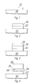
- FIG. 1 illustrates a tantalum sticking layer 32 deposited on the surface of a semiconductor body 30.
- Figure 2 illustrates a platinum/tantalum mixture layer 34 deposited on the tantalum sticking layer 32.
- the ratio of platinum to tantalum in the platinum/tantalum mixture layer 34 is, in this example, between 3:1 and 1:1.5.
- a method of forming this oxygen gettering layer 34 involves depositing the platinum and tantalum in the same process chamber using two sputter guns, so that the desired percentages of each metal are deposited, forming a mixture of the two metals.
- FIG 3 illustrates a platinum noble layer 36 deposited on the oxygen gettering layer 34.
- the three layers 32, 34, and 36 constitute the lower electrode of the capacitor.
- Figure 4 illustrates a barium strontium titanate layer 38 deposited on the platinum layer 36, and also the tantalum oxide particles 40 that are formed in the oxygen gettering layer 34 as a consequence of the barium strontium titanate layer 38 being deposited in a high temperature oxygen atmosphere.
- the lower electrode comprising layers 32, 34, and 36, remains electrically conductive after the barium strontium titanate deposition since the oxide particles 40 are spread throughout the oxygen gettering layer 34.
- the barium strontium titanate layer 38 constitutes the dielectric of the capacitor.
- Figure 5 illustrates a titanium nitride layer 42 deposited on the barium strontium titanate layer 38, forming the upper electrode of the capacitor.
- Figure 5 illustrates a planar geometry for all of the elements of the capacitor, this invention applies equally well to the construction of capacitor structures of more complicated geometries, including capacitors built into depressions in the semiconductor surface.
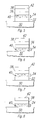
- such a capacitor structure may be formed without the tantalum layer 32 of Figure 5, and thus the oxygen gettering layer is preventing the oxidation of the top of the substrate.
- such a capacitor structure may be formed without the platinum layer 36 of Figure 5.
- such a capacitor structure may be formed without either the tantalum layer 32 or the platinum layer 36 of Figure 5.
- such a capacitor structure may be formed with a lower electrode comprising a graded layer 44 in which the amounts of each metal vary with respect to depth in the layer.
- the graded layer 44 is formed such that primarily tantalum is deposited near the semiconductor substrate, and then as the layer continues to be formed, the amount of platinum deposited is increased while the amount of tantalum deposited is decreased. Near the top of the layer, primarily platinum is deposited.
- such a capacitor may be formed with a lower electrode comprising a stratified region 46 between the tantalum layer 32 and the platinum layer 36.
- This stratified region 46 comprises relatively thin alternating layers of platinum and tantalum, which will intermix when heated, dispersing the tantalum into the platinum.
- the number and thickness of the layers in the stratified region 46 can be varied, depending on the amounts of tantalum and platinum required.
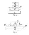
- Figure 10 depicts the lower electrode before application of the HDC material.
- the oxygen gettering layer 34 may be formed on an oxidizable layer 48.
- a platinum noble layer 36 is formed on the oxygen gettering layer 34, and a barium strontium titanate layer 38 is formed on the platinum layer 36, which causes the oxide particles 40 to form.
- the tantalum sticking layer 32 may be formed on a titanium nitride barrier layer 52, which is itself formed on a titanium silicide contact layer 50.
- the titanium nitride layer 52 and titanium silicide layer 50 are formed by depositing a thin layer of titanium on the silicon substrate 30, and then annealing in an NH 3 atmosphere.
- the titanium silicide layer 50 forms a low resistance contact to the underlying silicon substrate 30, while the titanium nitride layer 52 prevents the formation of insulating tantalum silicide between the silicon substrate 30 and the tantalum sticking layer 32.
- a tantalum plug 56 is formed through a silicon dioxide insulating layer 54, connecting the platinum/tantalum mixture layer 34 to the underlying silicon substrate 30.
- nitrides titanium nitride, zirconium nitride; silicides: titanium silicide, tantalum silicide, tungsten silicide, molybdenum silicide; carbides: tantalum carbide; borides: titanium boride) Conductive carbides and borides (e.g. boron carbide) 34 Oxygen gettering layer Platinum/ tantalum mixture wherein the ratio of platinum to tantalum is between 3:1 and 1:1.5 Noble metal/reactive metal mixtures wherein the ratio of noble metal to reactive metal is between 99:1 and 1:3 (e.g.
- platinum/tantalum mixtures platinum/tungsten mixtures, platinum/titanium mixtures
- Noble metal/reactive metal compound mixtures wherein the ratio of noble metal to reactive metal compound is between 99:1 and 1:3 (e.g. platinum/titanium nitride mixtures)
- Other combinations of above mentioned materials e.g. platinum/tantalum/tungsten mixture
- Other combinations of materials selected from Drawing Element 32 above and Drawing Element 36 below e.g. palladium/molybdenum mixtures
- Noble layer Platinum Other noble metals e.g.
- Barium strontium titanate Other transition metal titanates, tantalates, niobates, and zirconates (e.g. barium titanate, strontium titanate, lead zirconate titanate, lead zinc niobate)
- Other high dielectric constant oxides e.g. tantalum pentoxide
- Oxide particles Tantalum pentoxide Other oxides/suboxides of reactive metals and reactive metal compounds (e.g.
- palladium/molybdenum mixtures 46 Stratified region Alternating layers of platinum and tantalum wherein the thickness ratio of the platinum layers to the tantalum layers is between 3:1 and 1:1.5 Alternating layers of other noble and reactive metals wherein the thickness ratio of the noble metal layers to the reactive metal layers is between 99:1 and 1:3 (e.g. platinum/tantalum, platinum/tungsten, platinum/ titanium) Alternating layers of noble metal and reactive metal compound wherein the thickness ratio of the noble metal layers to the reactive metal compound layers is between 99:1 and 1:3 (e.g. platinum/titanium nitride) Other combinations of above mentioned materials (e.g.
- Compound semiconductors e.g. GaAs, Si/Ge, Si/C
- Contact layer Titanium silicide Other conductive silicides 52 Barrier layer Titanium nitride Other conductive nitrides Other high-temperature conductive diffusion barriers 54 Insulator Silicon dioxide Other insulators (e.g. silicon nitride) 56 Conductive Plug Tantalum Other reactive metals (e.g. tungsten, titanium, molybdenum) Reactive metal compounds (e.g.
- nitrides titanium nitride, zirconium nitride; silicides: titanium silicide, tantalum silicide, tungsten silicide, molybdenum silicide; carbides: tantalum carbide; borides: titanium boride) Conductive carbides and borides (e.g. boron carbide) Single component semiconductors (e.g. single crystalline and polycrystalline silicon, germanium) Compound semiconductors (e.g. GaAs, Si/Ge, Si/C)
Claims (17)
- Verfahren zum Bilden einer mikroelektronischen Struktur, das umfaßt:Bilden einer oxidierbaren Schicht (30, 32);Bilden einer Sauerstoffgetterschicht (34), die ein Gemisch aus wenigstens einer reaktiven Sauerstoffgetterkomponente und wenigstens einem nicht reaktiven Edelmetall umfaßt, auf der oxidierbaren Schicht (30, 32);Bilden einer Edelmetallschicht (30) auf der Sauerstoffgetterschicht (34); undBilden einer Schicht (38) aus einem Werkstoff mit hoher Dielektrizitätskonstante auf der Edelmetallschicht (36).
- Verfahren nach Anspruch 1, bei dem die Schicht (38) aus einem Werkstoff mit hoher Dielektrizitätskonstante durch einen Prozeß gebildet wird, der die reaktive Komponente der Sauerstoffgetterschicht (34) oxidiert.
- Verfahren nach Anspruch 1 oder Anspruch 2, das das Bilden einer elektrisch leitenden Schicht (42) auf der Schicht aus einem Werkstoff mit hoher Dielektrizitätskonstante umfaßt.
- Verfahren nach Anspruch 3, das das Auswählen der elektrisch leitenden Schicht (42) aus der Gruppe umfaßt, die aus Titannitrid, Rutheniumdioxid, YBa2Cu3O7-x, Platin, Palladium, Rhodium, Gold, Iridium, Silber und Kombinationen hiervon besteht.
- Verfahren nach einem vorhergehenden Anspruch, das das Bilden der Sauerstoffgetterschicht (34) in der Weise, daß das Verhältnis des Edelmetalls zur reaktiven Komponente zwischen etwa 99:1 und etwa 1:3 liegt, umfaßt.
- Verfahren nach Anspruch 5, das das Bilden der Sauerstoffgetterschicht (44), die eine abgestufte Mischung aus dem Edelmetall und der reaktiven Komponente enthält, umfaßt, wobei die reaktive Komponente in der Nähe der oxidierbaren Schicht (30, 32) mehr als 99% der Sauerstoffgetterschicht ausmacht und in der Weise variiert, daß sie in der Nähe der Edelmetallschicht (36) weniger als 1 % der Sauerstoffgetterschicht ausmacht.
- Verfahren nach Anspruch 5 oder Anspruch 6, das das Auswählen der reaktiven Komponente und der oxidierbaren Schicht (30, 32) aus der Gruppe umfaßt, die aus Tantal, Wolfram, Titan, Molybdän, Titannitrid, Zirkonnitrid, Titansilicid, Tantalsilicid, Wolframsilicid, Molybdänsilicid, Tantalcarbid, Titanborid, Borcarbid, Silizium, Germanium, Kohlenstoff, GaAs und Kombinationen hiervon besteht.
- Verfahren nach einem vorhergehenden Anspruch, das das Bilden der Edelmetallschicht aus der Gruppe umfaßt, die aus Platin, Palladium, Rhodium, Gold, Iridium, Silber und Kombinationen hiervon besteht.
- Verfahren nach einem vorhergehenden Anspruch, das das Auswählen des Werkstoffs (38) mit hoher Dielektrizitätskonstante aus der Gruppe umfaßt, die aus Barium-Strontium-Titanat, Bariumtitanat, Strontiumtitanat, Blei-Zirkon-Titanat, Blei-Zink-Niobat, Tantal-Pentoxid und Kombinationen hiervon besteht.
- Verfahren nach einem vorhergehenden Anspruch zum Bilden einer mikroelektronischen Kondensatorschicht.
- Mikroelektronische Struktur, die umfaßt:eine oxidierbare Schicht (30, 32);eine Sauerstoffgetterschicht (34, 44), die über der oxidierbaren Schicht (30, 32) liegt und ein Gemisch aus wenigstens einer reaktiven Sauerstoffgetterkomponente und wenigstens einer nicht reaktiven Edelmetallkomponente umfaßt;eine Edelmetallschicht (36), die über der Sauerstoffgetterschicht (34, 44) liegt; undeine Schicht aus einem Werkstoff (38) mit hoher Dielektrizitätskonstante, die über der Edelmetallschicht (36) liegt.
- Mikroelektronische Struktur nach Anspruch 11, bei der die reaktive Komponente wenigstens teilweise oxidiert ist und die Edelmetallkomponente eine elektrische Leitfähigkeit durch die Sauerstoffgetterschicht (34, 44) schafft.
- Mikroelektronische Struktur nach Anspruch 11 oder Anspruch 12, die eine elektrisch leitende Schicht (42) umfaßt, die vorzugsweise aus der Gruppe gewählt ist, die aus Titannitrid, Rutheniumdioxid, YBa2Cu3O7-x, Platin, Palladium, Rhodium, Gold, Iridium, Silber und Kombinationen hiervon besteht, und über der Schicht aus einem Werkstoff mit hoher Dielektrizitätskonstante liegt.
- Mikroelektronische Struktur nach einem der Ansprüche 11 bis 13, bei der das Verhältnis der Edelmetallkomponente zu der reaktiven Komponente in der Sauerstoffgetterschicht (34, 44) zwischen etwa 99:1 und etwa 1:3 liegt.
- Mikroelektronische Struktur nach Anspruch 14, bei der die Sauerstoffgetterschicht (44) eine abgestufte Mischung aus der Edelmetallkomponente und der reaktiven Komponente umfaßt, wobei die reaktive Komponente in der Nähe der oxidierbaren Schicht (30, 32) mehr als 99 % der Sauerstoffgetterschicht ausmacht und in der Weise variiert, daß sie in der Nähe der Edelmetallschicht (36) weniger als 1 % der Sauerstoffgetterschicht ausmacht.
- Mikroelektronische Struktur nach Anspruch 14 oder Anspruch 15, bei der die reaktive Komponente und die oxidierbare Schicht (30, 32) aus der Gruppe gewählt sind, die aus Tantal, Wolfram, Titan, Molybdän, Titannitrid, Zirkonnitrid, Titansilicid, Tantalsilicid, Wolframsilicid, Molybdänsilicid, Tantalcarbid, Titanborid, Borcarbid, Silicium, Germanium, Kohlenstoff, GaAs und Kombinationen hiervon besteht.
- Mikroelektronische Struktur nach einem der Ansprüche 11 bis 16, bei der der Werkstoff (38) mit hoher Dielektrizitätskonstante aus der Gruppe gewählt ist, die aus Barium-Strontium-Titanat, Bariumtitanat, Strontiumtitanat, Blei-Zirkon-Titanat, Blei-Zink-Niobat, Tantalpentoxid und Kombinationen hiervon besteht.
Applications Claiming Priority (2)
| Application Number | Priority Date | Filing Date | Title |
|---|---|---|---|
| US08/009,521 US5348894A (en) | 1993-01-27 | 1993-01-27 | Method of forming electrical connections to high dielectric constant materials |
| US9521 | 1993-01-27 |
Publications (3)
| Publication Number | Publication Date |
|---|---|
| EP0609081A2 EP0609081A2 (de) | 1994-08-03 |
| EP0609081A3 EP0609081A3 (de) | 1995-03-08 |
| EP0609081B1 true EP0609081B1 (de) | 2002-04-17 |
Family
ID=21738161
Family Applications (1)
| Application Number | Title | Priority Date | Filing Date |
|---|---|---|---|
| EP94300604A Expired - Lifetime EP0609081B1 (de) | 1993-01-27 | 1994-01-27 | Verbesserte elektrische Verbindungen zu dielektrischen Materialien |
Country Status (4)
| Country | Link |
|---|---|
| US (3) | US5348894A (de) |
| EP (1) | EP0609081B1 (de) |
| JP (1) | JPH077137A (de) |
| DE (1) | DE69430405T2 (de) |
Cited By (1)
| Publication number | Priority date | Publication date | Assignee | Title |
|---|---|---|---|---|
| US7319270B2 (en) | 2000-12-28 | 2008-01-15 | Infineon Technologies Ag | Multi-layer electrode and method of forming the same |
Families Citing this family (82)
| Publication number | Priority date | Publication date | Assignee | Title |
|---|---|---|---|---|
| JP3159561B2 (ja) * | 1993-03-29 | 2001-04-23 | ローム株式会社 | 結晶性薄膜用電極 |
| DE69404189T2 (de) * | 1993-03-31 | 1998-01-08 | Texas Instruments Inc | Leicht donatoren-dotierte Elektroden für Materialien mit hoher dielektrischer Konstante |
| JP3954635B2 (ja) * | 1994-01-13 | 2007-08-08 | ローム株式会社 | 誘電体キャパシタの製造方法 |
| JP3954339B2 (ja) * | 1994-01-13 | 2007-08-08 | ローム株式会社 | 誘電体キャパシタ |
| JP3954390B2 (ja) * | 1994-01-13 | 2007-08-08 | ローム株式会社 | 誘電体キャパシタ |
| JP3981142B2 (ja) * | 1994-01-13 | 2007-09-26 | ローム株式会社 | 強誘電体キャパシタおよびその製造方法 |
| DE4421007A1 (de) * | 1994-06-18 | 1995-12-21 | Philips Patentverwaltung | Elektronisches Bauteil und Verfahren zu seiner Herstellung |
| US5585300A (en) * | 1994-08-01 | 1996-12-17 | Texas Instruments Incorporated | Method of making conductive amorphous-nitride barrier layer for high-dielectric-constant material electrodes |
| US5622893A (en) * | 1994-08-01 | 1997-04-22 | Texas Instruments Incorporated | Method of forming conductive noble-metal-insulator-alloy barrier layer for high-dielectric-constant material electrodes |
| US5504041A (en) * | 1994-08-01 | 1996-04-02 | Texas Instruments Incorporated | Conductive exotic-nitride barrier layer for high-dielectric-constant materials |
| US5834374A (en) * | 1994-09-30 | 1998-11-10 | International Business Machines Corporation | Method for controlling tensile and compressive stresses and mechanical problems in thin films on substrates |
| KR0174594B1 (ko) * | 1994-11-26 | 1999-04-01 | 이재복 | 실리콘 웨이퍼상에 백금 박막을 형성하는 방법, 그 방법에 의하여 제조된 실리콘 기판 및 그 기판을 이용한 반도체 소자 |
| US6204111B1 (en) | 1994-12-28 | 2001-03-20 | Matsushita Electronics Corporation | Fabrication method of capacitor for integrated circuit |
| CN1075243C (zh) * | 1994-12-28 | 2001-11-21 | 松下电器产业株式会社 | 集成电路用电容元件及其制造方法 |
| US5563449A (en) * | 1995-01-19 | 1996-10-08 | Cornell Research Foundation, Inc. | Interconnect structures using group VIII metals |
| KR100214267B1 (ko) * | 1995-04-07 | 1999-08-02 | 김영환 | 반도체 소자 제조방법 |
| JP2751864B2 (ja) * | 1995-04-14 | 1998-05-18 | 日本電気株式会社 | 酸素拡散バリア性電極とその製造方法 |
| US5708302A (en) * | 1995-04-26 | 1998-01-13 | Symetrix Corporation | Bottom electrode structure for dielectric capacitors |
| US5663088A (en) | 1995-05-19 | 1997-09-02 | Micron Technology, Inc. | Method of forming a Ta2 O5 dielectric layer with amorphous diffusion barrier layer and method of forming a capacitor having a Ta2 O5 dielectric layer and amorphous diffusion barrier layer |
| US5745990A (en) * | 1995-06-06 | 1998-05-05 | Vlsi Technology, Inc. | Titanium boride and titanium silicide contact barrier formation for integrated circuits |
| CN1054702C (zh) * | 1995-06-26 | 2000-07-19 | 现代电子产业株式会社 | 制造半导体器件电容器的方法 |
| JP3929513B2 (ja) | 1995-07-07 | 2007-06-13 | ローム株式会社 | 誘電体キャパシタおよびその製造方法 |
| JP2795313B2 (ja) * | 1996-05-08 | 1998-09-10 | 日本電気株式会社 | 容量素子及びその製造方法 |
| US6025205A (en) * | 1997-01-07 | 2000-02-15 | Tong Yang Cement Corporation | Apparatus and methods of forming preferred orientation-controlled platinum films using nitrogen |
| US6054331A (en) * | 1997-01-15 | 2000-04-25 | Tong Yang Cement Corporation | Apparatus and methods of depositing a platinum film with anti-oxidizing function over a substrate |
| US6188120B1 (en) | 1997-02-24 | 2001-02-13 | International Business Machines Corporation | Method and materials for through-mask electroplating and selective base removal |
| US6498097B1 (en) | 1997-05-06 | 2002-12-24 | Tong Yang Cement Corporation | Apparatus and method of forming preferred orientation-controlled platinum film using oxygen |
| US5910880A (en) | 1997-08-20 | 1999-06-08 | Micron Technology, Inc. | Semiconductor circuit components and capacitors |
| US5989984A (en) * | 1997-10-07 | 1999-11-23 | Lucent Technologies, Inc. | Method of using getter layer to improve metal to metal contact resistance at low radio frequency power |
| JP3974697B2 (ja) * | 1997-11-28 | 2007-09-12 | ローム株式会社 | キャパシタおよびその製法 |
| US6191443B1 (en) | 1998-02-28 | 2001-02-20 | Micron Technology, Inc. | Capacitors, methods of forming capacitors, and DRAM memory cells |
| US6162744A (en) * | 1998-02-28 | 2000-12-19 | Micron Technology, Inc. | Method of forming capacitors having high-K oxygen containing capacitor dielectric layers, method of processing high-K oxygen containing dielectric layers, method of forming a DRAM cell having having high-K oxygen containing capacitor dielectric layers |
| US6111285A (en) * | 1998-03-17 | 2000-08-29 | Micron Technology, Inc. | Boride electrodes and barriers for cell dielectrics |
| US6156638A (en) | 1998-04-10 | 2000-12-05 | Micron Technology, Inc. | Integrated circuitry and method of restricting diffusion from one material to another |
| US6730559B2 (en) * | 1998-04-10 | 2004-05-04 | Micron Technology, Inc. | Capacitors and methods of forming capacitors |
| US6165834A (en) * | 1998-05-07 | 2000-12-26 | Micron Technology, Inc. | Method of forming capacitors, method of processing dielectric layers, method of forming a DRAM cell |
| US6255186B1 (en) | 1998-05-21 | 2001-07-03 | Micron Technology, Inc. | Methods of forming integrated circuitry and capacitors having a capacitor electrode having a base and a pair of walls projecting upwardly therefrom |
| DE19828969A1 (de) | 1998-06-29 | 1999-12-30 | Siemens Ag | Verfahren zur Herstellung von Halbleiterbauelementen |
| KR100403435B1 (ko) * | 1998-10-14 | 2003-10-30 | 가부시끼가이샤 히다치 세이사꾸쇼 | 반도체장치 및 그 제조방법 |
| US6038163A (en) * | 1998-11-09 | 2000-03-14 | Lucent Technologies Inc. | Capacitor loaded memory cell |
| DE19858357A1 (de) * | 1998-12-17 | 2000-06-29 | Siemens Ag | Mikroelektronische Struktur sowie Verfahren zu deren Herstellung |
| US20010013616A1 (en) * | 1999-01-13 | 2001-08-16 | Sailesh Mansinh Merchant | Integrated circuit device with composite oxide dielectric |
| US6235594B1 (en) | 1999-01-13 | 2001-05-22 | Agere Systems Guardian Corp. | Methods of fabricating an integrated circuit device with composite oxide dielectric |
| DE19901210A1 (de) * | 1999-01-14 | 2000-07-27 | Siemens Ag | Halbleiterbauelement und Verfahren zu dessen Herstellung |
| JP3211809B2 (ja) * | 1999-04-23 | 2001-09-25 | ソニー株式会社 | 半導体記憶装置およびその製造方法 |
| US6190963B1 (en) * | 1999-05-21 | 2001-02-20 | Sharp Laboratories Of America, Inc. | Composite iridium-metal-oxygen barrier structure with refractory metal companion barrier and method for same |
| US6943392B2 (en) * | 1999-08-30 | 2005-09-13 | Micron Technology, Inc. | Capacitors having a capacitor dielectric layer comprising a metal oxide having multiple different metals bonded with oxygen |
| US6197651B1 (en) | 1999-08-30 | 2001-03-06 | Taiwan Semiconductor Manufacturing Company | Structure and method for forming a capacitor dielectric using yttrium barium copper oxide |
| US6444478B1 (en) | 1999-08-31 | 2002-09-03 | Micron Technology, Inc. | Dielectric films and methods of forming same |
| DE19959711A1 (de) | 1999-12-10 | 2001-06-21 | Infineon Technologies Ag | Verfahren zur Herstellung einer strukturierten Metallschicht |
| US7005695B1 (en) | 2000-02-23 | 2006-02-28 | Micron Technology, Inc. | Integrated circuitry including a capacitor with an amorphous and a crystalline high K capacitor dielectric region |
| US6479857B1 (en) * | 2000-03-02 | 2002-11-12 | Lsi Logic Corporation | Capacitor having a tantalum lower electrode and method of forming the same |
| US6750502B1 (en) | 2000-03-21 | 2004-06-15 | Micron Technology, Inc. | Technique to quench electrical defects in aluminum oxide film |
| US6558517B2 (en) * | 2000-05-26 | 2003-05-06 | Micron Technology, Inc. | Physical vapor deposition methods |
| US6352921B1 (en) | 2000-07-19 | 2002-03-05 | Chartered Semiconductor Manufacturing Ltd. | Use of boron carbide as an etch-stop and barrier layer for copper dual damascene metallization |
| US6544801B1 (en) | 2000-08-21 | 2003-04-08 | Motorola, Inc. | Method of fabricating thermally stable MTJ cell and apparatus |
| US6451646B1 (en) * | 2000-08-30 | 2002-09-17 | Micron Technology, Inc. | High-k dielectric materials and processes for manufacturing them |
| US7378719B2 (en) * | 2000-12-20 | 2008-05-27 | Micron Technology, Inc. | Low leakage MIM capacitor |
| US6566147B2 (en) | 2001-02-02 | 2003-05-20 | Micron Technology, Inc. | Method for controlling deposition of dielectric films |
| US20030017266A1 (en) * | 2001-07-13 | 2003-01-23 | Cem Basceri | Chemical vapor deposition methods of forming barium strontium titanate comprising dielectric layers, including such layers having a varied concentration of barium and strontium within the layer |
| US6838122B2 (en) * | 2001-07-13 | 2005-01-04 | Micron Technology, Inc. | Chemical vapor deposition methods of forming barium strontium titanate comprising dielectric layers |
| US7011978B2 (en) * | 2001-08-17 | 2006-03-14 | Micron Technology, Inc. | Methods of forming capacitor constructions comprising perovskite-type dielectric materials with different amount of crystallinity regions |
| US7358171B2 (en) * | 2001-08-30 | 2008-04-15 | Micron Technology, Inc. | Method to chemically remove metal impurities from polycide gate sidewalls |
| US6545906B1 (en) | 2001-10-16 | 2003-04-08 | Motorola, Inc. | Method of writing to scalable magnetoresistance random access memory element |
| JP2003298134A (ja) * | 2002-01-31 | 2003-10-17 | Toyota Motor Corp | 積層型圧電アクチュエータ |
| US6936301B2 (en) * | 2002-05-06 | 2005-08-30 | North Carolina State University | Methods of controlling oxygen partial pressure during annealing of a perovskite dielectric layer |
| US7095646B2 (en) | 2002-07-17 | 2006-08-22 | Freescale Semiconductor, Inc. | Multi-state magnetoresistance random access cell with improved memory storage density |
| US7084813B2 (en) * | 2002-12-17 | 2006-08-01 | Ethertronics, Inc. | Antennas with reduced space and improved performance |
| US6898070B2 (en) | 2002-12-19 | 2005-05-24 | Avx Corporation | Transmission line capacitor |
| US6956763B2 (en) | 2003-06-27 | 2005-10-18 | Freescale Semiconductor, Inc. | MRAM element and methods for writing the MRAM element |
| US6967366B2 (en) | 2003-08-25 | 2005-11-22 | Freescale Semiconductor, Inc. | Magnetoresistive random access memory with reduced switching field variation |
| US7256980B2 (en) * | 2003-12-30 | 2007-08-14 | Du Pont | Thin film capacitors on ceramic |
| US7129098B2 (en) | 2004-11-24 | 2006-10-31 | Freescale Semiconductor, Inc. | Reduced power magnetoresistive random access memory elements |
| US20060169969A1 (en) * | 2005-02-02 | 2006-08-03 | Nanodynamics 88 | Bandgap cascade cold cathode |
| US7442319B2 (en) * | 2005-06-28 | 2008-10-28 | Micron Technology, Inc. | Poly etch without separate oxide decap |
| US20090152651A1 (en) * | 2007-12-18 | 2009-06-18 | International Business Machines Corporation | Gate stack structure with oxygen gettering layer |
| US7989321B2 (en) * | 2008-08-21 | 2011-08-02 | Taiwan Semiconductor Manufacturing Company, Ltd. | Semiconductor device gate structure including a gettering layer |
| US8679962B2 (en) * | 2008-08-21 | 2014-03-25 | Taiwan Semiconductor Manufacturing Company, Ltd. | Integrated circuit metal gate structure and method of fabrication |
| CN103545355A (zh) * | 2012-07-12 | 2014-01-29 | 中芯国际集成电路制造(上海)有限公司 | 半导体器件及其制作方法 |
| US9412940B2 (en) * | 2012-08-03 | 2016-08-09 | Ecole Polytechnique Federale De Lausanne (Epfl) | Resistive switching element and use thereof |
| EP3581904B1 (de) * | 2018-06-15 | 2021-06-02 | Melexis Technologies NV | Platinmetallisierung |
| US11178208B2 (en) | 2019-01-24 | 2021-11-16 | KLDiscovery Ontrack, LLC | Automatic initialization process for standalone e-discovery machine |
Family Cites Families (11)
| Publication number | Priority date | Publication date | Assignee | Title |
|---|---|---|---|---|
| US4471405A (en) * | 1981-12-28 | 1984-09-11 | International Business Machines Corporation | Thin film capacitor with a dual bottom electrode structure |
| US5194395A (en) * | 1988-07-28 | 1993-03-16 | Fujitsu Limited | Method of producing a substrate having semiconductor-on-insulator structure with gettering sites |
| US5005102A (en) * | 1989-06-20 | 1991-04-02 | Ramtron Corporation | Multilayer electrodes for integrated circuit capacitors |
| EP0415751B1 (de) * | 1989-08-30 | 1995-03-15 | Nec Corporation | Dünnfilmkondensator und dessen Herstellungsverfahren |
| NL9000602A (nl) * | 1990-03-16 | 1991-10-16 | Philips Nv | Werkwijze voor het vervaardigen van een halfgeleiderinrichting met geheugenelementen vormende condensatoren met een ferroelectrisch dielectricum. |
| JP2601022B2 (ja) * | 1990-11-30 | 1997-04-16 | 日本電気株式会社 | 半導体装置の製造方法 |
| JPH0746670B2 (ja) * | 1991-06-07 | 1995-05-17 | 日本電気株式会社 | 薄膜キャパシタ |
| JPH0746669B2 (ja) * | 1991-05-16 | 1995-05-17 | 日本電気株式会社 | 薄膜キャパシタ |
| JPH04359518A (ja) * | 1991-06-06 | 1992-12-11 | Nec Corp | 半導体装置の製造方法 |
| US5164808A (en) * | 1991-08-09 | 1992-11-17 | Radiant Technologies | Platinum electrode structure for use in conjunction with ferroelectric materials |
| US5187638A (en) * | 1992-07-27 | 1993-02-16 | Micron Technology, Inc. | Barrier layers for ferroelectric and pzt dielectric on silicon |
-
1993
- 1993-01-27 US US08/009,521 patent/US5348894A/en not_active Expired - Lifetime
-
1994
- 1994-01-26 JP JP6007170A patent/JPH077137A/ja active Pending
- 1994-01-27 EP EP94300604A patent/EP0609081B1/de not_active Expired - Lifetime
- 1994-01-27 DE DE69430405T patent/DE69430405T2/de not_active Expired - Fee Related
-
2000
- 2000-03-09 US US09/521,504 patent/US6215650B1/en not_active Expired - Lifetime
-
2001
- 2001-02-07 US US09/778,641 patent/US6275370B2/en not_active Expired - Fee Related
Cited By (1)
| Publication number | Priority date | Publication date | Assignee | Title |
|---|---|---|---|---|
| US7319270B2 (en) | 2000-12-28 | 2008-01-15 | Infineon Technologies Ag | Multi-layer electrode and method of forming the same |
Also Published As
| Publication number | Publication date |
|---|---|
| DE69430405T2 (de) | 2002-10-31 |
| US6215650B1 (en) | 2001-04-10 |
| US5348894A (en) | 1994-09-20 |
| US20010004790A1 (en) | 2001-06-28 |
| EP0609081A2 (de) | 1994-08-03 |
| US6275370B2 (en) | 2001-08-14 |
| JPH077137A (ja) | 1995-01-10 |
| EP0609081A3 (de) | 1995-03-08 |
| DE69430405D1 (de) | 2002-05-23 |
Similar Documents
| Publication | Publication Date | Title |
|---|---|---|
| EP0609081B1 (de) | Verbesserte elektrische Verbindungen zu dielektrischen Materialien | |
| EP0698918B1 (de) | Leitfähige Barriereschicht aus einer Legierung von Edelmetall und Isolator als Elektroden für Material mit hohen dielektrischen Konstanten | |
| EP0697720B1 (de) | Leitfähige Barriereschicht aus einem amorphen Nitrid als Elektrode für Material mit hoher dielektrischen Konstante | |
| US5679980A (en) | Conductive exotic-nitride barrier layer for high-dielectric-constant material electrodes | |
| US6593638B1 (en) | Lightly donor doped electrodes for high-dielectric-constant materials | |
| US6180447B1 (en) | Methods for fabricating integrated circuit capacitors including barrier layers having grain boundary filling material | |
| US5656852A (en) | High-dielectric-constant material electrodes comprising sidewall spacers | |
| US5581436A (en) | High-dielectric-constant material electrodes comprising thin platinum layers | |
| US5612574A (en) | Semiconductor structures using high-dielectric-constant materials and an adhesion layer | |
| US6362068B1 (en) | Electrode interface for high-dielectric-constant materials | |
| US5589284A (en) | Electrodes comprising conductive perovskite-seed layers for perovskite dielectrics | |
| EP0567062A1 (de) | Elektrische Verbindungen auf dielektrischen Materialien | |
| KR100355585B1 (ko) | 박막커패시터 | |
| US5440174A (en) | Plurality of passive elements in a semiconductor integrated circuit and semiconductor integrated circuit in which passive elements are arranged | |
| US6117689A (en) | Stable high-dielectric-constant material electrode and method | |
| JPH04366504A (ja) | 誘電体薄膜 | |
| KR100499429B1 (ko) | 마이크로일렉트로닉 구조물과 그의 제조 방법 및 용도 | |
| KR980012492A (ko) | 강유전체막을 구비하는 캐패시터 및 그 제조방법 | |
| KR0161451B1 (ko) | 반도체 기억장치 및 그 제조방법 | |
| JPH10135411A (ja) | 半導体装置 |
Legal Events
| Date | Code | Title | Description |
|---|---|---|---|
| PUAI | Public reference made under article 153(3) epc to a published international application that has entered the european phase |
Free format text: ORIGINAL CODE: 0009012 |
|
| AK | Designated contracting states |
Kind code of ref document: A2 Designated state(s): DE FR GB IT NL |
|
| RIN1 | Information on inventor provided before grant (corrected) |
Inventor name: SUMMERFELT, SCOTT R. Inventor name: GNADE,BRUCE E. |
|
| PUAL | Search report despatched |
Free format text: ORIGINAL CODE: 0009013 |
|
| AK | Designated contracting states |
Kind code of ref document: A3 Designated state(s): DE FR GB IT NL |
|
| 17P | Request for examination filed |
Effective date: 19950814 |
|
| 17Q | First examination report despatched |
Effective date: 19960913 |
|
| GRAG | Despatch of communication of intention to grant |
Free format text: ORIGINAL CODE: EPIDOS AGRA |
|
| GRAG | Despatch of communication of intention to grant |
Free format text: ORIGINAL CODE: EPIDOS AGRA |
|
| GRAH | Despatch of communication of intention to grant a patent |
Free format text: ORIGINAL CODE: EPIDOS IGRA |
|
| REG | Reference to a national code |
Ref country code: GB Ref legal event code: IF02 |
|
| GRAH | Despatch of communication of intention to grant a patent |
Free format text: ORIGINAL CODE: EPIDOS IGRA |
|
| GRAA | (expected) grant |
Free format text: ORIGINAL CODE: 0009210 |
|
| AK | Designated contracting states |
Kind code of ref document: B1 Designated state(s): DE FR GB IT NL |
|
| PG25 | Lapsed in a contracting state [announced via postgrant information from national office to epo] |
Ref country code: NL Free format text: LAPSE BECAUSE OF FAILURE TO SUBMIT A TRANSLATION OF THE DESCRIPTION OR TO PAY THE FEE WITHIN THE PRESCRIBED TIME-LIMIT Effective date: 20020417 Ref country code: IT Free format text: LAPSE BECAUSE OF FAILURE TO SUBMIT A TRANSLATION OF THE DESCRIPTION OR TO PAY THE FEE WITHIN THE PRESCRIBED TIME-LIMIT;WARNING: LAPSES OF ITALIAN PATENTS WITH EFFECTIVE DATE BEFORE 2007 MAY HAVE OCCURRED AT ANY TIME BEFORE 2007. THE CORRECT EFFECTIVE DATE MAY BE DIFFERENT FROM THE ONE RECORDED. Effective date: 20020417 |
|
| REF | Corresponds to: |
Ref document number: 69430405 Country of ref document: DE Date of ref document: 20020523 |
|
| ET | Fr: translation filed | ||
| NLV1 | Nl: lapsed or annulled due to failure to fulfill the requirements of art. 29p and 29m of the patents act | ||
| PLBE | No opposition filed within time limit |
Free format text: ORIGINAL CODE: 0009261 |
|
| STAA | Information on the status of an ep patent application or granted ep patent |
Free format text: STATUS: NO OPPOSITION FILED WITHIN TIME LIMIT |
|
| 26N | No opposition filed |
Effective date: 20030120 |
|
| PGFP | Annual fee paid to national office [announced via postgrant information from national office to epo] |
Ref country code: DE Payment date: 20080131 Year of fee payment: 15 |
|
| PGFP | Annual fee paid to national office [announced via postgrant information from national office to epo] |
Ref country code: FR Payment date: 20080107 Year of fee payment: 15 |
|
| PGFP | Annual fee paid to national office [announced via postgrant information from national office to epo] |
Ref country code: GB Payment date: 20081211 Year of fee payment: 16 |
|
| PG25 | Lapsed in a contracting state [announced via postgrant information from national office to epo] |
Ref country code: DE Free format text: LAPSE BECAUSE OF NON-PAYMENT OF DUE FEES Effective date: 20090801 |
|
| REG | Reference to a national code |
Ref country code: FR Ref legal event code: ST Effective date: 20091030 |
|
| PG25 | Lapsed in a contracting state [announced via postgrant information from national office to epo] |
Ref country code: FR Free format text: LAPSE BECAUSE OF NON-PAYMENT OF DUE FEES Effective date: 20090202 |
|
| GBPC | Gb: european patent ceased through non-payment of renewal fee |
Effective date: 20100127 |
|
| PG25 | Lapsed in a contracting state [announced via postgrant information from national office to epo] |
Ref country code: GB Free format text: LAPSE BECAUSE OF NON-PAYMENT OF DUE FEES Effective date: 20100127 |