EP0600434B1 - Semiconductor memory device - Google Patents
Semiconductor memory device Download PDFInfo
- Publication number
- EP0600434B1 EP0600434B1 EP93119267A EP93119267A EP0600434B1 EP 0600434 B1 EP0600434 B1 EP 0600434B1 EP 93119267 A EP93119267 A EP 93119267A EP 93119267 A EP93119267 A EP 93119267A EP 0600434 B1 EP0600434 B1 EP 0600434B1
- Authority
- EP
- European Patent Office
- Prior art keywords
- memory cell
- logic voltage
- bit line
- data
- plate electrode
- Prior art date
- Legal status (The legal status is an assumption and is not a legal conclusion. Google has not performed a legal analysis and makes no representation as to the accuracy of the status listed.)
- Expired - Lifetime
Links
Images


Classifications
-
- G—PHYSICS
- G11—INFORMATION STORAGE
- G11C—STATIC STORES
- G11C11/00—Digital stores characterised by the use of particular electric or magnetic storage elements; Storage elements therefor
- G11C11/21—Digital stores characterised by the use of particular electric or magnetic storage elements; Storage elements therefor using electric elements
- G11C11/22—Digital stores characterised by the use of particular electric or magnetic storage elements; Storage elements therefor using electric elements using ferroelectric elements
-
- G—PHYSICS
- G11—INFORMATION STORAGE
- G11C—STATIC STORES
- G11C5/00—Details of stores covered by group G11C11/00
- G11C5/06—Arrangements for interconnecting storage elements electrically, e.g. by wiring
- G11C5/063—Voltage and signal distribution in integrated semi-conductor memory access lines, e.g. word-line, bit-line, cross-over resistance, propagation delay
Definitions
- the present invention relates to a semiconductor memory device.
- a semiconductor memory device chiefly operates on a method of accumulating electric charges in a capacitor formed in the semiconductor device, and storing the data depending on the presence or absence of electric charge (generally called dynamic random access memory or DRAM).
- DRAM dynamic random access memory
- a silicon oxide film is generally used as an insulation film.
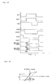
- Fig. 24 is a circuit diagram of a conventional semiconductor memory device
- Fig. 25 is an operation timing chart of the semiconductor memory device of Fig. 24
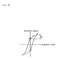
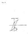
- Fig. 26 is a diagram showing the hysteresis characteristic of ferrodielectric element used in the main body cell capacitor in the conventional semiconductor memory device of Fig. 26,
- Fig. 27 is a diagram showing the hysteresis characteristic of the ferrodielectric element used in a dummy cell capacitor in the conventional semiconductor memory device.
- bit lines 26, 28 are connected to a sense amplifier 30.
- Main body memory cells 20a, 20b, 20c and 20d, 20e, and dummy memory cells 46 and 36 are connected to the bit lines 26 and 28, respectively.
- the main body memory cell 20a is composed of a MOS transistor 24 and a main body memory cell capacitor 22.
- the gate of the MOS transistor 24 is connected to a word line 32, the drain of the MOS transistor 24 is connected to the bit line 26, and the source of the MOS transistor 24 is connected to a first electrode of the main body memory cell capacitor 22.
- a second electrode of the main body memory cell capacitor 22 is connected to a cell plate electrode 34.
- the dummy memory cell 36 is composed of a MOS transistor 38 and a dummy memory cell capacitor 40.
- the gate of the MOS transistor 38 is connected to a dummy word line 42
- the drain of the MOS transistor 38 is connected to the bit line 28, and the source of the MOS transistor 38 is connected to a first electrode of the dummy memory cell capacitor 40.
- a second electrode of the dummy memory cell capacitor 40 is connected to a dummy cell plate electrode 44.
- Fig. 26 and Fig. 27 are the hysteresis characteristic diagrams of the ferrodielectric element.
- the axis of abscissas denotes the electric force applied to the memory cell capacitor, and the axis of ordinates represents the electric charge at that time.
- the electric force is 0, the residual polarization is left over as indicated at point B, point E, point K, and point H. After turning off the power source, too, a residual polarization occurs in the ferrodielectric capacitor.
- the main body memory cell capacity is in the state of point B in Fig.
- the initial state of the dummy memory cell capacitor is the state of point K in Fig. 27.
- the logic voltages of the bit lines 26 and 28, word line 32, dummy word line 42, cell plate electrode 34, and dummy cell plate electrode 44 are set to L. Later, the bit lines 26 and 28 are set in floating state.
- the word line 32, dummy word line 42, cell plate electrode 34, and dummy cell plate 44 are all set to logic voltage H.
- the MOS transistors 24 and 38 are turned on, and electric force is applied to the main body memory cell capacitor 22 and dummy memory cell capacitor 40.
- the state at point B in Fig. 26 is changed to the state at point D, and an electric charge Q1 is read out in the bit line 26.
- the state at point E in Fig. 26 is changed to the state at point D, and an electric charge Q0 is read out in the bit line 26.
- the dummy memory cell changes from the state at point K in Fig.
- the data of the main body memory cell read out in the bit line 26 and the data of the dummy memory cell read out in the bit line 28 are amplified by the sense amplifier 30, and the data in the main body memory cell are read out.
- the bit line 26 is at logic voltage H
- the cell plate electrode 34 is at logic voltage H. Accordingly, electric force is not applied to the main body memory cell capacitor 22, thereby coming in the state at point E in Fig. 26.
- the logic voltage of the cell plate electrode 34 is set to L, and is once to set the state at point A in Fig. 26, and the logic voltage of the word line 32 is set to L.
- the word line 32 is at logic voltage L
- electric force is not applied to the main body memory cell capacitor 22, thereby returning to the state at point B in Fig. 26.
- the bit line 26 comes to the logic voltage L
- the cell plate electrode 34 comes to the logic voltage H. Accordingly, the main body memory cell capacitor 22 is in the state of point D in Fig. 26.
- the cell plate electrode 34 is at logic voltage L, electric force is not applied to the main body memory cell capacitor 22, thereby coming to the state of point E in Fig. 26.
- the logic voltage of the word line 32 comes at L, and electric force is not applied yet to the main body memory cell capacitor 22, thereby remaining at the state of point E in Fig. 26.
- the bit line 28 is at the logic voltage L
- the cell plate electrode 44 is at the logic voltage H. Accordingly, the dummy memory cell capacitor 40 is in the state of point J in Fig. 27. Later, when the dummy word line 36 is at the logic voltage L, electric force is not applied to the dummy memory cell capacitor 40, thereby returning to the state of point K in Fig. 27.
- the bit line 28 is at the logic voltage H
- the cell plate electrode 44 is at the logic voltage H. Accordingly, the dummy memory cell capacitor 40 is in the state at point K in Fig. 27.
- the dummy word line 36 is later set to the logic voltage L
- the logic voltage of the dummy cell plate electrode 44 is set to L at the same time, the state of no application of electric force in the dummy cell memory capacitor 40 is unchanged, and the state at point K in Fig. 27 is maintained.
- the dummy memory cell capacitor does not always become state of point K in Fig. 27.
- the initial state is the state of point H in Fig. 27, the problem was that malfunction occurred in the first reading.
- the dummy word line 42 and dummy cell plate electrode 44 are simultaneously set to the logic voltage L. Therefore, for example, if the parasitic capacity of the dummy word line 42 is large and the fall of the dummy word line 42 is later than the fall of the dummy cell plate electrode, at the time of "0" of the data of the main body memory cell, the bit line 28 comes to the logic voltage H, and the cell plate electrode 44 comes to the logic voltage L. Hence, the dummy memory cell capacitor 40 comes to the state of point G in Fig. 27.
- the dummy memory cell capacitor 40 comes to the state of point H in Fig. 27.
- the problem was that malfunction occurred at the next time of reading out the memory cell.
- the present invention concerns a semiconductor memory device comprising : an amplifier, a first bit line and a second bit line being connected to this amplifier, a first ferroelectric capacitor, a first MOS transistor having its gate connected to a first word line, a first electrode of the first ferroelectric capacitor is connected to the source of said first MOS transistor, and said first bit line is connected to the drain of said first MOS transistor, a second electrode of the first ferroelectric capacitor being connected to a first plate electrode, a second ferroelectric capacitor, and a second MOS transistor having its gate connected to a second word line, a first electrode of the second ferroelectric capacitor is connected to the source of said second MOS transistor, and said second bit line is connected to the drain of said second MOS transistor, a second electrode of the second ferroelectric capacitor being connected to a second plate electrode, which is characterized by means for initializing the electric charge state of said second ferroelectric capacitor to a residual polarization point at which no electric field exists across said second ferroelectric
- the semiconductor memory device may further comprise means for inverting the logic voltage of the first plate electrode and second plate electrode after turning off the second MOS transistor, and then turning off the first MOS transistor.
- the semiconductor memory device further comprises means for setting the second bit line at a certain logic voltage, turning on the second MOS transistor, and then setting the logic voltage of the second plate electrode to a reverse value of the logic voltage of the second bit line, before start or after end of writing or reading action of memory cell data.
- the present invention concerns a semiconductor memory device comprising : an amplifier, a first bit line and a second bit line being connected to this amplifier, a first ferroelectric capacitor, a first MOS transistor having its gate connected to a first word line, a first electrode of said first ferroelectric capacitor is connected to the source of said first MOS transistor, and the first bit line is connected to the drain of said first MOS transistor, a second electrode of said first ferroelectric capacitor being connected to a first plate electrode, a second ferroelectric capacitor, and a second MOS transistor having its gate connected to a second word line, a first electrode of the second ferroelectric capacitor is connected to the source of said second MOS transistor, and the second bit line is connected to the drain of said second MOS transistor, a second electrode of said second ferroelectric capacitor being connected to a second plate electrode, and a third MOS transistor having its gate connected to a data initializing control signal line, a data initializing potential signal line is connected to the source of said third MOS transistor, and the first electrode
- the semiconductor memory device may be such that the first plate electrode and the second plate electrode are connected.
- the semiconductor memory device may be such that the data initializing potential signal line is connected to the grounding potential.
- the semiconductor memory device may further comprise means for making the logic voltage of the first bit line and the logic voltage of the second bit line be both grounding potential, before start of writing or reading action of the memory cell data.
- the semiconductor memory device may further comprise means for turning on the third MOS transistor after turning off the second MOS transistor, and inverting the logic voltage of the first plate electrode and the second plate electrode, then turning off the first MOS transistor.
- the semiconductor memory device may further comprise means for making the logic voltage of the first plate electrode be an inverse logic voltage of the logic voltage of the first bit line before start of reading action of the memory cell data.
- the semiconductor memory device may further comprise means for making the logic voltage of the second plate electrode and the logic voltage of the first electrode of the second ferroelectric capacitor be reverse logic voltages of the logic voltage of the second bit line before start of reading action of the memory cell data.
- the semiconductor memory device may further comprise means for making the logic voltage of the second plate electrode and the logic voltage of the second bit line be inverse logic voltages of the logic voltage of the first electrode of the second ferroelectric capacitor before start of reading action of the memory cell data.
- the semiconductor memory device may further comprise means for making at least one of the logic voltage of the first plate electrode and the logic voltage of the second plate electrode (DCP0) be always the same value.
- the semiconductor memory device may further comprise means for inverting the logic voltages of the first plate electrode and the second plate electrode after turning on the first MOS transistor and the second MOS transistor.
- the semiconductor memory device may further comprise means for precharging of the first bit line and the second bit line into one logic voltage action of the memory cell data after turning on the first MOS transistor and the second MOS transistor, and then inverting the logic voltages of the first plate electrode and second plate electrode (DCP0).
- the semiconductor memory device may further comprise means for turning on the first MOS transistor and second MOS transistor after inverting the logic voltages of the first plate electrode and the second plate electrode.
- the dummy memory cell capacitor can be initialized, and malfunction in reading is eliminated. Besides, the state of the dummy memory cell capacitor after reading the data can be securely set to the initial state, and malfunction in reading does not occur. A semiconductor memory device without concentration of power consumption is also realized.
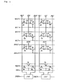
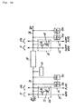
- Fig. 1 is a diagram showing a circuit configuration of a first embodiment of a semiconductor memory device of the invention.
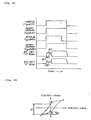
- Fig. 2 is a diagram showing the operation timing in the first embodiment of the semiconductor memory device of the invention.
- Fig. 3 is a diagram showing a circuit configuration of a second embodiment of a semiconductor memory device of the invention.
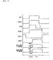
- Fig. 4 is a diagram showing the operation timing in the second embodiment of the semiconductor memory device of the invention.
- Fig. 5 is a diagram showing the operation timing in a third embodiment of a semiconductor memory device of the invention.
- Fig. 6 is a diagram showing a circuit configuration of a fourth embodiment of a semiconductor memory device of the invention.
- Fig. 7 is a diagram showing the operation timing in the fourth embodiment of the semiconductor memory device of the invention.
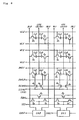
- Fig. 8 is a diagram showing a circuit configuration of a fifth embodiment of a semiconductor memory device of the invention.
- Fig. 9 is a diagram showing the operation timing in the fifth embodiment of the semiconductor memory device of the invention.
- Fig. 10 is a diagram showing the hysteresis characteristic of ferrodielectric element of a main body memory cell capacitor used in the fifth embodiment of the semiconductor memory device of the invention.
- Fig. 11 is a diagram showing the hysteresis characteristic of ferrodielectric element of a dummy memory cell capacitor used in the fifth embodiment of the semiconductor memory device of the invention.
- Fig. 12 is a diagram showing a circuit configuration of a sixth embodiment of a semiconductor memory device of the invention.
- Fig. 13 is a diagram showing the operation timing in the sixth embodiment of the semiconductor memory device of the invention.
- Fig. 14 is a diagram showing a circuit configuration of a seventh embodiment of a semiconductor memory device of the invention.
- Fig. 15 is a diagram showing the operation timing in the seventh embodiment of the semiconductor memory device of the invention.
- Fig. 16 is a diagram showing a circuit configuration of an eighth embodiment of a semiconductor memory device of the invention.
- Fig. 17 is a diagram showing the operation timing in the eighth embodiment of the semiconductor memory device of the invention.
- Fig. 18 is a diagram showing the operation timing in a ninth embodiment of a semiconductor memory device of the invention.
- Fig. 19 is a diagram showing the hysteresis characteristic of ferrodielectric element of a main body memory cell capacitor used in the ninth embodiment of the semiconductor memory device of the invention.
- Fig. 20 is a diagram showing the hysteresis characteristic of ferrodielectric element of a dummy memory cell capacitor used in the ninth embodiment of the semiconductor memory device of the invention.
- Fig. 21 is a diagram showing the operation timing in a tenth embodiment of a semiconductor memory device of the invention.
- Fig. 22 is a diagram showing the operation timing in an eleventh embodiment of a semiconductor memory device of the invention.
- Fig. 23 is a diagram showing the operation timing in a twelfth embodiment of a semiconductor memory device of the invention.
- Fig. 24 is a diagram showing a circuit configuration of a conventional semiconductor memory device.
- Fig. 25 is a diagram showing the operation timing of a conventional semiconductor memory device.
- Fig. 26 is a diagram showing the hysteresis characteristic of ferrodielectric element of a main body memory cell capacitor used in a conventional semiconductor memory device.
- Fig. 27 is a diagram showing the hysteresis characteristic of ferrodielectric element of a dummy memory cell capacitor used in a conventional semiconductor memory device.
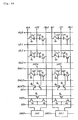
- Fig. 1 shows a first embodiment of the invention.
- a main body memory cell is composed of main body memory cell ferrodielectric capacitors Cs1 to Cs8, and N-channel type MOS transistors Qn having word lines WL0 to WL3 connected to the gates thereof.
- the first electrodes of the main body memory cell ferrodielectric capacitors Cs1 to Cs8 are connected to the sources of the N-channel type MOS transistors Qn.
- the second electrodes of the main body memory cell ferrodielectric capacitors Cs1 to Cs8 are connected to either cell plate electrode CP0 or CP1.
- the drains of the N-channel type MOS transistors Qn composing the main body memory cell are connected to any one of bit lines BL0, /BL0, BL1, /BL1.
- a dummy memory cell is similarly composed of dummy memory cell ferrodielectric capacitors Cd1 to Cd4, and N-channel type MOS transistors Qn having dummy word lines DWL0 to DWL1 connected to the gates thereof.
- the first electrodes of the dummy memory cell ferrodielectric capacitors Cd1 to Cd4 are connected to the sources of the N-channel type MOS transistors Qn.
- the second electrodes of the dummy memory cell ferrodielectric capacitors Cd1 to Cd4 are connected to either one of dummy cell plate electrodes DCP0 and DCP1.
- the drains of the N-channel type MOS transistors Qn for composing the dummy memory cell are connected to any one of bit lines BL0, /BL0, BL1, /BL1.
- the sets of bit lines BL0 and /BL0, and BL1 and /BL1 are respectively connected to the sense amplifiers SA0, SA1.
- the sense amplifiers SA0, SA1 are controlled by sense amplifier control signals SAE0, SAE1, respectively, and they operate when SAE0, SAE1 are logic voltage H.
- bit lines BL0 and /BL0, and BL1 and /BL1 are connected through the N-channel type MOS transistors Qn having bit line equalizing and precharging control signals EQ11 applied to the gates thereof, and the bit lines BL0, /BL0, BL1, and /BL1 are connected to a grounding voltage VSS through the N-channel type MOS transistors Qn having bit line equalizing and precharging control signals EQ11 applied to the gates thereof.
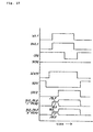
- Fig. 2 is an operation timing chart of the first embodiment.
- the ferrodielectric element of the main body memory cell capacitor possesses the hysteresis characteristic shown in Fig. 26, and the ferrodielectric element of the dummy memory cell capacitor possesses the hysteresis characteristic shown in Fig. 27.
- the word lines, dummy word lines, cell plate electrodes, dummy cell plate electrodes, and sense amplifier control signals are set at logic voltage L
- the bit line equalizing and precharging control signals EQ11 are set at logic voltage H
- the bit lines are set at logic voltage L.
- the bit line equalizing and precharging control signals EQ11 are set at logic voltage L
- the bit lines are set in floating state.
- the dummy memory cell changes from the state at point K to the state at point J in Fig. 27, and the electric charge Qd is read out in the bit line.
- setting the sense amplifying control signal SAE0 at logic voltage H the sense amplifier SA0 is operated, and the data being read out in the bit lines BL0, /BL0 are amplified.
- the cell plate electrode CP0 is set at the logic voltage L. At this time, when the data of the main body memory cell is 1, it comes to be in the state of point A in Fig. 26. When the data of the main body memory cell is 0, the state is point E in Fig. 26.
- the word line WL1 and dummy word line DWL1 are set at logic voltage L. At this time, if the data of the main body memory cell is 1, it comes to be in the state of point A or point B in Fig. 26, or when the data of the main body memory cell is 0, it becomes the state of point E in Fig. 26.
- the dummy cell plate electrode CP0 is set at logic voltage L, the sense amplifier control signal SAE0 at logic voltage L, the bit line equalizing and precharging control signal EQ11 at logic voltage H, and the bit line at logic voltage L.
- the initial state of the dummy memory cell can be securely set in the state at point K in Fig. 27, by setting the dummy cell plate electrode at logic voltage L after setting the dummy word line at logic voltage L. Therefore, malfunction does not occur at the next time of data reading.
- the dummy word line is set to logic voltage L after setting the dummy cell plate electrode at logic voltage L, in the case that the main body memory cell data is 0, when the dummy cell plate electrode becomes logic voltage L, the dummy memory cell is in the state of point G in Fig. 27.
- the dummy word line comes to logic voltage L, the dummy memory cell is in the state of point G or point H in Fig. 27.
- the initial state of the dummy memory cell is not the state of point K in Fig. 27, malfunction occurs at the next time of data reading.
- Fig. 3 shows a second embodiment.
- a main body memory cell is composed of main body memory cell ferrodielectric capacitors Cs1 to Cs8, and N-channel type MOS transistors Qn having word lines WL0 to WL3 connected to the gates thereof.
- the first electrodes of the main body memory cell ferrodielectric capacitors Cs1 to Cs8 are connected to the sources of the N-channel type MOS transistors Qn, and the second electrodes of the main body memory cell ferrodielectric capacitors Cs1 to Cs8 are connected to either cell plate electrode CP0 (DCP0) or CP1 (DCP1).
- the drains of the N-channel type MOS transistors Qn composing the main body memory cell are connected to any one of bit lines BL0, /BL0, BL1, /BL1.
- a dummy memory cell is similarly composed of dummy memory cell ferrodielectric capacitors Cd1 to Cd4, and N-channel type MOS transistors Qn having dummy word lines DWL0 to DWL1 connected to the gates thereof.
- the first electrodes of the dummy memory cell ferrodielectric capacitors Cd1 to Cd4 are connected to the sources of the N-channel type MOS transistors Qn, and the second electrodes of the dummy memory cell ferrodielectric capacitors Cd1 to Cd4 are connected to either one of cell plate electrodes CP0 (DCP0) and CP1 (DCP1).
- the drains of the N-channel type MOS transistors Qn for composing the dummy memory cell are connected to any one of bit lines BL0, /BL0, BL1, /BL1.
- the sets of bit lines BL0 and /BL0, and BL1 and /BL1 are respectively connected to the sense amplifiers SA0, SA1.
- the sense amplifiers SA0, SA1 are controlled by sense amplifier control signals SAE0, SAE1, respectively, and they operate when SAE0, SAE1 are logic voltage H.
- the bit lines BL0 and /BL0, and BL1 and /BL1 are connected through the N-channel type MOS transistors Qn having bit line equalizing and precharging control signals EQ21 applied to the gates thereof.
- the bit lines BL0, /BL0, BL1, and /BL1 are connected to a grounding voltage VSS through the N-channel type MOS transistors Qn having bit line equalizing and precharging control signals EQ21 applied to the gates thereof.
- Fig. 4 is an operation timing chart of the second embodiment.
- the ferrodielectric element of the main body memory cell capacitor possesses the hysteresis characteristic shown in Fig. 26, and the ferrodielectric element of the dummy memory cell capacitor possesses the hysteresis characteristic shown in Fig. 27.
- the word lines, dummy word lines, cell plate electrodes, dummy cell plate electrodes, and sense amplifier control signals are set at logic voltage L
- the bit line equalizing and precharging control signals EQ21 are set at logic voltage H
- the bit lines are set at logic voltage L.
- the bit line equalizing and precharging control signals EQ21 are set at logic voltage L
- the bit lines are set in floating state.
- the dummy memory cell changes from the state at point K to the state at point J in Fig. 27, and the electric charge Qd is read out in the bit line.
- setting the sense amplifying control signal SAE0 at logic voltage H the sense amplifier SA0 is operated, and the data being read out in the bit lines BL0, /BL0 are amplified.
- the cell plate electrode CP0 (DCP0) is set at the logic voltage L.
- the sense amplifier control signal SAE0 is set at logic voltage L, the bit line equalizing and precharging control signal EQ21 at logic voltage H, and the bit line at logic voltage L.
- the initial state of the dummy memory cell can be securely set in the state at point K in Fig. 27, by setting the (dummy) cell plate electrode at logic voltage L after setting the dummy word line at logic voltage L.
- the cell plate electrode of the main body memory cell and the dummy cell plate electrode of the dummy memory cell can be commonly used.
- Fig. 3 The circuit diagram of the third embodiment of the invention is shown in Fig. 3, which is same as that of the second embodiment.
- Fig. 5 shows the operation timing diagram.
- the logic voltage of the sense amplifier control signal SAE0 is set to L
- the bit line equalizing and precharging control signal EQ21 is set to logic voltage H
- the bit line is set to logic voltage L
- reading of data of the main memory cell is terminated.
- the operation is so far same as in the second embodiment.
- the dummy word line DWL1 and cell plate electrode CP0 (DCP0) are set to logic voltage H. This is the timing of initialization of the data of the dummy memory cell, and the state of the dummy memory cell is the state at point J in Fig. 27.
- the state of the dummy memory cell becomes the state at point K in Fig. 27.
- the data of the dummy memory cell can be securely initialized to the state at point K in Fig. 27, by the timing action of initialization of the data of the dummy memory cell.
- the dummy memory cell may not be always in the initial sate, and this is used in such a case.
- the dummy memory cell since the dummy memory cell is initialized at the last step of a series of action timing of reading of data, the dummy memory cell cannot be initialized without performing reading action.
- Fig. 6 shows the fourth embodiment.
- the main body memory cell is composed of main body memory cell ferrodielectric capacitors Cs1 to Cs8, and N-channel type MOS transistors Qn having word lines WL0 to WL3 connected to the gates thereof.
- the first electrodes of the main body memory cell ferrodielectric capacitors Cs1 to Cs8 are connected to the sources of the N-channel type MOS transistors Qn, and the second electrodes of the main body memory cell ferrodielectric capacitors Cs1 to Cs8 are connected to either cell plate electrode CP0 (DCP0) or CP1 (DCP1).
- the drains of the N-channel type MOS transistors Qn composing the main body memory cell are connected to any one of bit lines BL0, /BL0, BL1, /BL1.
- a dummy memory cell is similarly composed of dummy memory cell ferrodielectric capacitors Cd1 to Cd4, and N-channel type MOS transistors Qn having dummy word lines DWL0 to DWL1 connected to the gates thereof.
- the first electrodes of the dummy memory cell ferrodielectric capacitors Cd1 to Cd4 are connected to the sources of the N-channel type MOS transistors Qn, and the second electrodes of the dummy memory cell ferrodielectric capacitors Cd1 to Cd4 are connected to either one of cell plate electrodes CP0 (DCP0) and CP1 (DCP1).
- the first electrodes of the dummy memory cell ferrodielectric capacitors Cd1 to Cd4 are connected to a data initializing potential signal line DIS41 through the N-channel type MOS transistors Qn, which is a dummy memory cell data initializing control signal DCW41, at the gate.
- the data initializing potential signal line is connected to the grounding voltage VSS.
- the drains of the N-channel type MOS transistors Qn for composing the dummy memory cell are connected to any one of bit lines BL0, /BL0, BL1, /BL1.
- the sets of bit lines BL0 and /BL0, and BL1 and /BL1 are respectively connected to the sense amplifiers SA0, SA1.
- the sense amplifiers SA0, SA1 are controlled by sense amplifier control signals SAE0, SAE1, respectively, and they operate when SAE0, SAE1 are logic voltage H.
- the bit lines BL0 and /BL0, and BL1 and /BL1 are connected through the N-channel type MOS transistors Qn having bit line equalizing and precharging control signals EQ41 applied to the gates thereof.
- the bit lines BL0, /BL0, BL1, and /BL1 are connected to a grounding voltage VSS through the N-channel type MOS transistors Qn having bit line equalizing and precharging control signals EQ41 applied to the gates thereof.
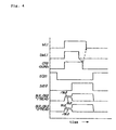
- Fig. 7 is a diagram showing the operation timing of the fourth embodiment.
- the ferrodielectric element of the main body memory capacitor possesses the hysteresis characteristic as shown in Fig. 26, and the ferrodielectric element of the dummy memory cell capacitor presents the hysteresis characteristic as shown in Fig. 27.
- the word line, dummy word line, cell plate electrode, dummy cell plate electrode, and sense amplifier control signal are set to logic voltage L, the dummy memory cell data initializing control signal DCW41 at logic voltage H, and the data of the dummy memory cell at initial state of K in Fig. 27.
- the bit line equalizing and precharging control signal EQ41 is set at logic voltage H, and the bit line at logic voltage L. Later, the bit line equalizing and precharging control signal EQ41 is set at logic voltage L, and the bit line is set in floating state.
- the dummy memory cell data initializing control signal DCW41 is set at logic voltage L, and the first electrode of the dummy memory cell ferrodielectric capacitor is set in floating state.
- the word line WL1, dummy word line DWL 1, and cell plate electrode CP0 (DCP0) are set at logic voltage H, the data of the dummy memory cell is read out in bit line BL0, and the data of the main body memory cell is read out in bit line /BL0.
- the state at point B in Fig. 26 is changed to the state at point D, and the electric charge Q1 is read out in the bit line.
- the state at point E in Fig. 26 is changed to the state at point D, and the electric charge Q0 is read out in the bit line.
- the dummy memory cell is changed from the state of point K to the state of point J in Fig. 27, and the electric charge Qd is read out in the bit line.
- the sense amplifier control signal SAE0 is set at logic voltage H to operate the sense amplifier SA0, and the data being read out in the bit lines BL0, /BL0 is amplified.
- the dummy word line DWL1 is set at logic voltage L.
- the dummy memory cell data initializing control signal DCW41 is set at logic voltage H, and the dummy memory cell is set in the state of point J in Fig. 27.
- the cell plate electrode CP0 (DCP0) is set at logic voltage L.
- the word line WL1 is set at logic voltage L.
- the state is either point A or point B in Fig. 26.
- the state is point E in Fig. 26.
- the sense amplifier control signal SAE0 is set at logic voltage L
- the bit line equalizing and precharging control signal EQ21 is set at logic voltage H
- the bit line is set at logic voltage L.
- the initial state of the dummy memory cell can be set to the state of point K in Fig. 27, by controlling the state of the first electrode of the dummy memory cell ferrodielectric capacitor by the dummy memory cell data initializing control signal DCW41.
- the cell plate electrode CP0 (DCP0) is set at logic voltage L, so that the initial state of the dummy memory cell can be securely set to the state of point K in Fig. 27.
- the cell plate electrode CP0 (DCP0) is set at logic voltage L, and therefore when the cell plate electrode CP0 (DCP0) is changed by a certain potential, the first electrode is in floating state, and it may not change by the same potential.
- the fourth embodiment since the first electrode of the memory cell and the cell plate electrode are both set at the grounding potential, the potentials are the same unless there is potential difference between the two electrodes.
- the precharging potential of the bit line is the grounding voltage VSS (logic voltage L)
- the initial state of the first electrode of the dummy memory cell ferrodielectric capacitor is at the grounding voltage VSS (logic voltage L)
- VCC supply voltage
- Fig. 8 shows the fifth embodiment of the invention.
- the fifth embodiment is same as the fourth embodiment in the circuit configuration, but is opposite to the fourth embodiment in the logic voltage of the initial state of the bit line, cell plate electrode and dummy memory cell.
- the main body memory cell is composed of main body memory cell ferrodielectric capacitors Cs1 to Cs8, and N-channel type MOS transistors Qn having word lines WL0 to WL3 connected to the gates thereof.
- the first electrodes of the main body memory cell ferrodielectric capacitors Cs1 to Cs8 are connected to the sources of the N-channel type MOS transistors Qn, and the second electrodes of the main body memory cell ferrodielectric capacitors Cs1 to Cs8 are connected to either cell plate electrode CP0 (DCP0) or CP1 (DCP1).
- the drains of the N-channel type MOS transistors Qn composing the main body memory cell are connected to any one of bit lines BL0, /BL0, BL1, /BL1.
- a dummy memory cell is similarly composed of dummy memory cell ferrodielectric capacitors Cd1 to Cd4, and N-channel type MOS transistors Qn having dummy word lines DWL0 to DWL1 connected to the gates thereof.
- the first electrodes of the dummy memory cell ferrodielectric capacitors Cd1 to Cd4 are connected to the sources of the N-channel type MOS transistors Qn, and the second electrodes of the dummy memory cell ferrodielectric capacitors Cd1 to Cd4 are connected to either one of cell plate electrodes CP0 (DCP0) and CP1 (DCP1).
- the first electrodes of the dummy memory cell ferrodielectric capacitors Cd1 to Cd4 are connected to a data initializing potential signal line DIS51 through the N-channel type MOS transistors Qn, which is a dummy memory cell data initializing control signal DCW51, at the gate.
- the data initializing potential signal line is connected to the grounding voltage VSS.
- the drains of the N-channel type MOS transistors Qn for composing the dummy memory cell are connected to any one of bit lines BL0, /BL0, BL1, /BL1.
- the sets of bit lines BL0 and /BL0, and BL1 and /BL1 are respectively connected to the sense amplifiers SA0, SA1.
- the sense amplifiers SA0, SA1 are controlled by sense amplifier control signals SAE0, SAE1, respectively, and they operate when SAE0, SAE1 are logic voltage H.
- the bit lines BL0 and /BL0, and BL1 and /BL1 are connected through the N-channel type MOS transistors Qn having bit line equalizing and precharging control signals EQ51 applied to the gates there
- the bit lines BL0, /BL0, BL1, and /BL1 are connected to a grounding voltage VSS through the N-channel type MOS transistors Qn having bit line equalizing and precharging control signals EQ51 applied to the gates thereof.
- Fig. 9 is a diagram showing the operation timing of the fifth embodiment.
- Fig. 10 is a diagram showing the hysteresis characteristic of ferrodielectric element of the main body memory cell capacitor in the semiconductor memory device, and
- Fig. 11 is a diagram showing the hysteresis characteristic of ferrodielectric element of the dummy memory cell capacitor.
- the word line, dummy word line and sense amplifier control signal are set at logic voltage L, cell plate electrode and dummy cell plate electrode at logic voltage H, and the dummy memory cell data initializing control signal DCW51 at logic voltage L.
- the bit line equalizing and precharging control signal EQ51 is set at logic voltage L, and the m-bit line at logic voltage H. Later, the bit line equalizing and precharging control signal EQ51 is set at logic voltage H, and the bit line is set in floating state.
- the dummy memory cell data initializing control signal DCW51 is set at logic voltage H, and the first electrode of the dummy memory cell ferrodielectric capacitor is set in floating state.
- the word line WL1 and dummy word line DWL1 are set at logic voltage H, and cell plate electrode CP0 (DCP0) is set at logic voltage L
- the data of the dummy memory cell is read out in bit line BL0
- the data of the main body memory cell is read out in bit line /BL0.
- the state at point B in Fig. 10 is changed to the state at point A, and the electric charge Q1 is read out in the bit line.
- the state at point E in Fig. 10 is changed to the state at point A, and the electric charge Q0 is read out in the bit line.
- the dummy memory cell is changed from the state of point H to the state of point G in Fig. 11, and the electric charge Qd is read out in the bit line.
- the sense amplifier control signal SAE0 is set at logic voltage H to operate the sense amplifier SA0, and the data being read out in the bit lines BL0, /BL0 is amplified.
- the dummy word line DWL1 is set at logic voltage L.
- the dummy memory cell data initializing control signal DCW51 is set at logic voltage L, and the dummy memory cell is set in the state of point G in Fig. 11.
- the cell plate electrode CP0 (DCP0) is set at logic voltage H. At this time, if the data of the main body memory cell is 1. the state is point A in Fig. 10. When the data of the main body memory cell is 0, the state is point D in Fig. 10, and the dummy memory cell is in the state of point H in Fig. 11.
- the word line WL1 is set at logic voltage L.
- the state is either point A or point B in Fig. 10.
- the state is point E in Fig. 10.
- the sense amplifier control signal SAE0 is set at logic voltage L
- the bit line equalizing and precharging control signal EQ51 is set at logic voltage H
- the bit line is set at logic voltage H.
- the initial state of the dummy memory cell can be securely set to the state of point H in Fig. 11, by controlling the state of the first electrode of the dummy memory cell ferrodielectric capacitor by the dummy memory cell data initializing control signal DCW51.
- Fig. 12 shows the sixth embodiment of the invention.
- a main body memory cell is composed of main body memory cell ferrodielectric capacitors Cs1 to Cs8, and N-channel type MOS transistors Qn having word lines WL0 to WL3 connected to the gates thereof.
- the first electrodes of the main body memory cell ferrodielectric capacitors Cs1 to Cs8 are connected to the sources of the N-channel type MOS transistors Qn, and the second electrodes of the main body memory cell ferrodielectric capacitors Cs1 to Cs8 are connected to either cell plate electrode CP0 or CP1.
- the drains of the N-channel type MOS transistors Qn composing the main body memory cell are connected to any one of bit lines BL0, /BL0, BL1, /BL1.
- a dummy memory cell is similarly composed of dummy memory cell ferrodielectric capacitors Cd1 to Cd4, and N-channel type MOS transistors Qn having dummy word lines DWL0 to DWL1 connected to the gates thereof.
- the first electrodes of the dummy memory cell ferrodielectric capacitors Cd1 to Cd4 are connected to the sources of the N-channel type MOS transistors Qn, and the second electrodes of the dummy memory cell ferrodielectric capacitors Cd1 to Cd4 are connected to either one of dummy cell plate electrodes DCP0 and DCP1.
- the first electrodes of the dummy memory cell ferrodielectric capacitors Cd1 to Cd4 are connected to a supply voltage VCC through the N-channel type MOS transistor Qn, which is the dummy memory cell data initializing control signal DCW61, at the gate.
- the drains of the N-channel type MOS transistors Qn for composing the dummy memory cell are connected to any one of bit lines BL0, /BL0, BL1, /BL1.
- the sets of bit lines BL0 and /BL0, and BL1 and /BL1 are respectively connected to the sense amplifiers SA0, SA1.
- the sense amplifiers SA0, SA1 are controlled by sense amplifier control signals SAE0, SAE1, respectively, and they operate when SAE0, SAE1 are logic voltage H.
- the sets of bit lines BL0 and /BL0, and BL1 and /BL1 are connected through the N-channel type MOS transistors Qn of which gates are bit line equalizing and precharging control signals EQ61.
- the bit lines BL0, /BL0, BL1, and /BL1 are connected to a grounding voltage VSS through the N-channel type MOS transistors Qn of which gates are bit line equalizing and precharging control signals EQ61.
- the operation of the semiconductor memory device is described while referring to the operation timing in Fig. 13.
- the ferrodielectric element of the main body memory cell capacitor is represented by the hysteresis characteristic shown in Fig. 26, and the ferrodielectric element of the dummy memory cell capacitor by the hysteresis characteristic shown in Fig. 27.
- the word lines, dummy word lines and sense amplifier control signals are set at logic voltage L, cell plate electrodes and dummy cell plate electrodes at logic voltage H, and the dummy memory cell data initializing control signal DCW61 at logic voltage H.
- the data of the dummy memory cell is the state at point K in Fig. 27, which is an initial state.
- the bit line equalizing and precharging control signal EQ61 is set at the logic voltage H, and the bit wire is set at logic voltage L.
- the bit line equalizing and precharging control signals EQ61 are set at logic voltage L, and the bit lines are set in floating state.
- the dummy memory cell data initializing control signal DCW61 is set at logic voltage L, and the first electrode of the dummy memory cell ferrodielectric capacitor is set in floating state.
- the word line WL1 and dummy word line DWL1 are set at logic voltage H.
- the data in the dummy memory cell is read out into the bit line BL0, and the data of the main body memory cell is read out in the bit line /BL0.
- the electric charge Q1 is readout in the bit line.
- the electric charge Q0 is read out in the bit line.
- the dummy memory cell changes from the state at point K to the state at point J in Fig. 27, and the electric charge Qd is read out in the bit line. Then, setting the sense amplifying control signal SAE0 at logic voltage H, the sense amplifier SA0 is operated, and the data being read out in the bit lines BL0, /BL0 are amplified.
- the cell plate electrode CP0 is set at the logic voltage L.
- the data of the main body memory cell is 1, it comes to be in the state of point A in Fig. 26.
- the state is point E in Fig. 26.
- the word line WL1 and dummy word line DWL1 are set at logic voltage L, the cell plate electrode CP0 at logic voltage H, and the dummy memory cell data initializing control signal DCW61 at logic voltage H.
- the sense amplifier control signal SAE0 is set at logic voltage L, the bit line equalizing and precharging control signal EQ61 at logic voltage H, and the bit line at logic voltage L.
- the data can be read out from the main body memory cell and dummy memory cell directly into the bit line, when the word lines and dummy word lines are set at logic voltage H, by setting, as the initial state for reading out the data of the main body memory cell, the logic voltage of the bit lines and the logic voltage of the cell plate electrodes at opposite logic voltages in the main body memory cell, and the logic voltage of the bit lines and the logic voltage of the first electrode of the dummy memory cell ferrodielectric capacitor at opposite logic voltages in the dummy memory cell.
- the cell plate since the cell plate has the capacity of memory cell, it takes time until the cell plate potential is changed to the logic voltage H. Accordingly, it takes a long time to read out the data.
- the cell plate electrode since the cell plate electrode is initially at logic voltage H, the data can be read out immediately by setting the word line and dummy word line at logic voltage H.
- the data reading electric charge of the dummy memory cell plate is the data reading electric charge Qd of the dummy memory cell of the difference between state at point K and state at point J in Fig. 27.
- the inclination of the curve is slight near point J, and the amount of change of the electric charge for the change of electric force is small. Accordingly, if sufficient electric force is not applied when reading out, the electric charge is in saturated state for the electric force near point J. That is, the error of data reading electric charge Qd of the dummy memory cell is small.
- Fig. 14 shows the seventh embodiment of the invention.
- the seventh embodiment is similar to the sixth embodiment, except that the transistor having the dummy memory cell data initializing control signal DCW71 connected to its gate is a P-channel type MOS transistor Qp.
- a main body memory cell is composed of main body memory cell ferrodielectric capacitors Cs1 to Cs8, and N-channel type MOS transistors Qn having word lines WL0 to WL3 connected to the gates thereof.
- the first electrodes of the main body memory cell ferrodielectric capacitors Cs1 to Cs8 are connected to the sources of the N-channel type MOS transistors Qn, and the second electrodes of the main body memory cell ferrodielectric capacitors Cs1 to Cs8 are connected to either cell plate electrode CP0 or CP1.
- the drains of the N-channel type MOS transistors Qn composing the main body memory cell are connected to any one of bit lines BL0, /BL0, BL1, /BL1.
- a dummy memory cell is similarly composed of dummy memory cell ferrodielectric capacitors Cd1 to Cd4, and N-channel type MOS transistors Qn having dummy word lines DWL0 to DWL1 connected to the gates thereof.
- the first electrodes of the dummy memory cell ferrodielectric capacitors Cd1 to Cd4 are connected to the sources of the N-channel type MOS transistors Qn, and the second electrodes of the dummy memory cell ferrodielectric capacitors Cd1 to Cd4 are connected to either one of dummy cell plate electrodes DCP0 and DCP1.
- the first electrodes of the dummy memory cell ferrodielectric capacitors Cd1 to Cd4 are connected to a supply voltage VCC through the P-channel type MOS transistor Qp, which is the dummy memory cell data initializing control signal DCW71, at the gate.
- the drains of the N-channel type MOS transistors Qn for composing the dummy memory cell are connected to any one of bit lines BL0, /BL0, BL1, /BL1.
- the sets of bit lines BL0 and /BL0, and BL1 and /BL1 are respectively connected to the sense amplifiers SA0, SA1.
- the sense amplifiers SA0, SA1 are controlled by sense amplifier control signals SAE0, SAE1, respectively, and they operate when SAE0, SAE1 are logic voltage H.
- the sets of bit lines BL0 and /BL0, and BL1 and BL1 are connected through the N-channel type MOS transistors Qn of which gates are bit line equalizing and precharging control signals EQ71.
- the bit lines BL0, /BL0, BL1, and /BL1 are connected to a grounding voltage VSS through the N-channel type MOS transistors Qn of which gates are bit line equalizing and precharging control signals EQ71.
- the operation of the semiconductor memory device is described while referring to the operation timing in Fig. 15.
- the ferrodielectric element of the main body memory cell capacitor shows the hysteresis characteristic shown in Fig. 26, and the ferrodielectric element of the dummy memory cell capacitor shows the hysteresis characteristic shown in Fig. 27.
- the word lines, dummy word lines and sense amplifier control signals are set at logic voltage L, cell plate electrodes and dummy cell plate electrodes at logic voltage H, and the dummy memory cell data initializing control signal DCW71 at logic voltage L.
- the data of the dummy memory cell is the state at point K in Fig. 27, which is an initial state.
- the bit line equalizing and precharging control signal EQ71 is set at the logic voltage H, and the bit wire is set at logic voltage L.
- the bit line equalizing and precharging control signals EQ71 are set at logic voltage L, and the bit lines are set in floating state.
- the dummy memory cell data initializing control signal DCW71 is set at logic voltage H, and the first electrode of the dummy memory cell ferrodielectric capacitor is set in floating state.
- the word line WL1 and dummy word line DWL1 are set at logic voltage H, and hence the data in the dummy memory cell is read out into the bit line BL0, and the data of the main body memory cell is read out in the bit line /BL0.
- the electric charge Q1 is read out in the bit line.
- the electric charge Q0 is read out in the bit line.
- the dummy memory cell changes from the state at point K to the state at point J in Fig. 27, and the electric charge Qd is read out in the bit line. Then, setting the sense amplifying control signal SAE0 at logic voltage H, the sense amplifier SA0 is operated, and the data being read out in the bit lines BL0, /BL0 are amplified.
- the cell plate electrode CP0 is set at the logic voltage L.
- the state is point E in Fig. 26.
- the word line WL1 and dummy word line DWL1 are set at logic voltage L, the cell plate electrode CP0 at logic voltage H, and the dummy memory cell data initializing control signal DCW71 at logic voltage L.
- the data of the main body memory cell is 1, it comes to be in the state of point A or point B in Fig. 26.
- the sense amplifier control signal SAE0 is set at logic voltage L
- the bit line equalizing and precharging control signal EQ71 at logic voltage H
- the bit line at logic voltage L is set at logic voltage L
- the data can be read out from the main body memory cell and dummy memory cell directly into the bit line, when the word lines and dummy word lines are set at logic voltage H, by setting, as the initial state for reading out the data of the main body memory cell, the logic voltage of the bit lines and the logic voltage of the cell plate electrodes at opposite logic voltages in the main body memory cell, and the logic voltage of the bit lines and the logic voltage of the first electrode of the dummy memory cell ferrodielectric capacitor at opposite logic voltages in the dummy memory cell.
- the dummy cell plate electrode is fixed at the logic voltage H, it leads to saving of power consumption of the semiconductor memory device.
- data reading of the dummy memory cell is the data reading electric charge Qd of the dummy memory cell as the difference between point K and point J in Fig. 27, but if sufficient electric force is not applied in reading, the electric charge is in saturated state for the electric force near point J, so that error of data reading electric charge Qd of the dummy memory cell is small.
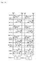
- Fig. 16 shows the eighth embodiment of the invention.
- a main body memory cell is composed of main body memory cell ferrodielectric capacitors Cs1 to Cs8, and N-channel type MOS transistors Qn having word lines WL0 to WL3 connected to the gates thereof.
- the first electrodes of the main body memory cell ferrodielectric capacitors Cs1 to Cs8 are connected to the sources of the N-channel type MOS transistors Qn, and the second electrodes of the main body memory cell ferrodielectric capacitors Cs1 to Cs8 are connected to cell plate electrodes CP0 to CP3.
- the drains of the N-channel type MOS transistors Qn composing the main body memory cell are connected to any one of bit lines BL0, /BL0, /BL0, BL1, /BL1.
- a dummy memory cell is similarly composed of dummy memory cell ferrodielectric capacitors Cd1 to Cd4, and N-channel type MOS transistors Qn having dummy word lines DWL0 to DWL1 connected to the gates thereof.
- the first electrodes of the dummy memory cell ferrodielectric capacitors Cd1 to Cd4 are connected to the sources of the N-channel type MOS transistors Qn, and the second electrodes of the dummy memory cell ferrodielectric capacitors Cd1 to Cd4 are connected to either one of dummy cell plate electrodes DCP0 and DCP1.
- the first electrodes of the dummy memory cell ferrodielectric capacitors Cd1 to Cd4 are connected to a supply voltage VCC through the N-channel type MOS transistor Qn, which is the dummy memory cell data initializing control signal DCW81, at the gate.
- the drains of the N-channel type MOS transistors Qn for composing the dummy memory cell are connected to any one of bit lines BL0, /BL0, BL1, /BL1.
- the sets of bit lines BL0 and /BL0, and BL1 and /BL1 are respectively connected to the sense amplifiers SA0, SA1.
- the sense amplifiers SA0, SA1 are controlled by sense amplifier control signals SAE0, SAE1, respectively, and they operate when SAE0, SAE1 are logic voltage H.
- the sets of bit lines BL0 and /BL0, and BL1 and /BL1 are connected through the N-channel type MOS transistors Qn of which gates are bit line equalizing and precharging control signals EQ81.
- the bit lines BL0, /BL0, BL1, and /BL1 are connected to a grounding voltage VSS through the N-channel type MOS transistors Qn of which gates are bit line equalizing and precharging control signals EQ81.
- the cell plate electrodes of the memory cell capacitors of the main body memory cell that are selected by one word line are always the same. That is, it is designed to read all of the data in the main body memory cell selected by one word line.
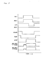
- the operation of the semiconductor memory device is described while referring to the operation timing in Fig. 17.
- the ferrodielectric element of the main body memory cell capacitor shows the hysteresis characteristic shown in Fig. 26, and the ferrodielectric element of the dummy memory cell capacitor shows the hysteresis characteristic shown in Fig. 27.
- the word line WL1, dummy word line DWL1 and sense amplifier control signals are set at logic voltage L, cell plate electrode CP1 and dummy cell plate electrode DCP1 at logic voltage H, and the dummy memory cell data initializing control signal DCW81 at logic voltage H.
- the data of the dummy memory cell is the state at point K in Fig. 27, which is an initial state
- the bit line equalizing and precharging control signal EQ81 is set at the logic voltage H, and the bit wire is set at logic voltage L.
- the bit line equalizing and precharging control signals EQ81 are set at logic voltage L, and the bit lines are set in floating state.
- the dummy memory cell data initializing control signal DCW81 is set at logic voltage L, and the first electrode of the dummy memory cell ferrodielectric capacitor is set in floating state.
- the word line WL1 and dummy word line DWL1 are set at logic voltage H.
- the data in the dummy memory cell is read out into the bit line BL0, and the data of the main body memory cell is read out in the bit line /BL0.
- the electric charge Q1 is read out in the bit line.
- the electric charge Q0 is read out in the bit line.
- the dummy memory cell changes from the state at point K to the state at point J in Fig. 27, and the electric charge Qd is read out in the bit line. Then, setting the sense amplifying control signal SAE0, SAE1 at logic voltage H, the sense amplifiers SA0, SA1 are operated, and the data being read out in the bit lines BL0, /BL0 are amplified.
- the cell plate electrode CP1 is set at the logic voltage L. At this time, when the data of the main body memory cell is 1, it comes to be in the state of point A in Fig. 26, and when the data of the main body memory cell is 0, the state is point E in Fig. 26.
- the word line WL1 and dummy word line DWL1 are set at logic voltage L, the cell plate electrode CP1 at logic voltage H, and the dummy memory cell data initializing control signal DCW81 at logic voltage H.
- the sense amplifier control signals SAE0, SAE1 are set at logic voltage L, the bit line equalizing and precharging control signal EQ81 at logic voltage H, and the bit line at logic voltage L.
- the data can be read out from the main body memory cell and dummy memory cell directly into the bit line, when the word lines and dummy word lines are set at logic voltage H, by setting, as the initial state for reading out the data of the main body memory cell, the logic voltage of the bit lines and the logic voltage of the cell plate electrodes at opposite logic voltages in the main body memory cell, and the logic voltage of the bit lines and the logic voltage of the first electrode of the dummy memory cell ferrodielectric capacitor at opposite logic voltages in the dummy memory cell. Moreover, since the dummy cell plate electrode can be fixed at logic voltage H, the power consumption of the semiconductor memory device can be saved. In the eighth embodiment, the data of the main body memory cell selected by one word line can be read out either partly or completely.
- the ninth embodiment of the invention is described below while referring to the circuit diagram in Fig. 12 and the operation timing in Fig. 18.
- the circuit diagram in Fig. 12 is same as that of the sixth embodiment.
- the ferrodielectric element of the main body memory cell capacitor shows the hysteresis characteristic in Fig. 19, and the ferrodielectric element of the dummy memory cell capacitor shows the hysteresis characteristic in Fig. 20.
- the word lines, dummy word lines, sense amplifier control signals, and dummy cell plate electrodes are set at logic voltage L, cell plate electrodes and dummy cell plate electrodes at logic voltage H, and the dummy memory cell data initializing control signal DCW61 at logic voltage H.
- the data of the dummy memory cell is the state at point G in Fig. 20, which is an initial state.
- the bit line equalizing and precharging control signal EQ61 is set at the logic voltage H, and the bit wire is set at logic voltage L.
- the bit line equalizing and precharging control signals EQ61 are set at logic voltage L, and the bit lines are set in floating state.
- the dummy memory cell data initializing control signal DCW61 is set at logic voltage L, and the first electrode of the dummy memory cell ferrodielectric capacitor is set in floating state.
- the word line WL1 and dummy word line DWL1 are set at logic voltage H, and the data in the dummy memory cell is read out into the bit line BL0, and the data of the main body memory cell is read out in the bit line /BL0.
- the electric charge Q1 is read out in the bit line.
- the electric charge Q0 is read out in the bit line.
- the dummy memory cell is changed from the state of point G to point H in Fig. 20, and the electric charge Qd is read in the bit line. Then, setting the sense amplifying control signal SAE0 at logic voltage H, the sense amplifier SA0 is operated, and the data being read out in the bit lines BL0, /BL0 are amplified.
- the cell plate electrode CP0 is set at the logic voltage L.
- the data of the main body memory cell is 1, it comes to be in the state of point A in Fig. 19, and when the data of the main body memory cell is 0, the state is point E in Fig. 19.
- the word line WL1 and dummy word line DWL1 are set at logic voltage L, the cell plate electrode CP0 at logic voltage H, and the dummy memory cell data initializing control signal DCW61 at logic voltage H.
- the sense amplifier control signal SAE0 is set at logic voltage L, the bit line equalizing and precharging control signal EQ61 at logic voltage H, and the bit line at logic voltage L.
- the data can be read out from the main body memory cell and dummy memory cell directly into the bit line, when the word lines and dummy word lines are set at logic voltage H, by setting, as the initial state for reading out the data of the main body memory cell, the logic voltage of the bit lines and the logic voltage of the cell plate electrodes at opposite logic voltages in the main body memory cell, and the logic voltage of the bit lines and the logic voltage of the first electrode of the dummy memory cell ferrodielectric capacitor at opposite logic voltages in the dummy memory cell. Moreover, since the dummy cell plate electrode can be fixed at logic voltage L, the power consumption of the semiconductor memory device can be saved.
- the tenth embodiment of the invention is described below by referring to the circuit diagram in Fig. 6 and the operation timing in Fig. 21.
- the circuit diagram in Fig. 6 is same as in the fourth embodiment.
- the ferrodielectric element of the main body memory cell capacitor shows the hysteresis characteristic in Fig. 26, and the ferrodielectric element of the dummy memory cell capacitor shows the hysteresis characteristic in Fig. 27.
- the word line, dummy word line, cell plate electrode, dummy cell plate electrode, and sense amplifier control signal are set to logic voltage L, and the dummy memory cell data initializing control signal DCW41 is at logic voltage H.
- the data of the dummy memory cell at initial state of K in Fig. 27.
- the bit line equalizing and precharging control signal EQ41 is set at logic voltage H, and the bit line at logic voltage L.
- the bit line equalizing and precharging control signal EQ41 is set at logic voltage L, and the bit line is set in floating state.
- the dummy memory cell data initializing control signal DCW41 is set at logic voltage L, and the first electrode of the dummy memory cell ferrodielectric capacitor is set in floating state.
- the word line WL1 and dummy word line DWL1 are set at logic voltage H, and the cell plate electrode CP0 (DCP0) is set at logic voltage H, and hence the data in the dummy memory cell is read out into the bit line BL0, and the data of the main body memory cell is read out in the bit line /BL0.
- the electric charge Q1 is read out in the bit line.
- the electric charge Q0 is read out in the bit line.
- the dummy memory cell changes from the state at point K to the state at point J in Fig. 27, and the electric charge Qd is read out in the bit line.
- setting the sense amplifying control signal SAE0 at logic voltage H the sense amplifier SA0 is operated, and the data being read out in the bit lines BL0, /BL0 are amplified.
- the dummy word line DWL1 is set at logic voltage L.
- the dummy memory cell data initializing control signal DCW41 is set at logic voltage H, and the dummy memory cell is set in the state of point J in Fig. 27.
- the cell plate electrode CP0 (DCP0) is set at the logic voltage L.
- the data of the main body memory cell is 1, it comes to be in the state of point A in Fig. 26.
- the state is point E in Fig. 26.
- the dummy memory cell is in the state of point K in Fig. 27.
- the word line WL1 is set at logic voltage L. At this time, if the data of the main body memory cell is 1, it comes to be in the state of point A or point B in Fig. 26. Or, when the data of the main body memory cell is 0, it becomes the state of point E in Fig. 26. Next, the sense amplifier control signal SAE0 is set at logic voltage L, the bit line equalizing and precharging control signal EQ21 at logic voltage H, and the bit line at logic voltage L.
- the current consumption is dispersed by deviating the rise time of the word lines and dummy word lines, and the rise time of the cell plate electrode CP0 (DCP0).
- the eleventh embodiment of the invention is described below by referring to the circuit diagram in Fig. 6 and the operation timing in Fig. 22.
- the circuit diagram in Fig. 6 is same as in the fourth embodiment.
- the ferrodielectric element of the main body memory cell capacitor shows the hysteresis characteristic in Fig. 26, and the ferrodielectric element of the dummy memory cell capacitor shows the hysteresis characteristic in Fig.27.
- the word line, dummy word line, cell plate electrode, dummy cell plate electrode, and sense amplifier control signal are set to logic voltage L, and the dummy memory cell data initializing control signal DCW41 is at logic voltage H.
- the bit line equalizing and precharging control signal EQ41 is set at logic voltage H, and the bit line at logic voltage L.
- the dummy memory cell data initializing control signal DCW41 is set at logic voltage L, and the first electrode of the dummy memory cell ferrodielectric capacitor is set in floating state.
- the word line WL1 and dummy word line DWL1 are set at logic voltage H, and the bit line equalizing and precharging control signal EQ41 is set at L, and the bit line is set in floating state.
- the cell plate electrode CP0 (DCP0) is set at logic voltage H, the data in the dummy memory cell is read out into the bit line BL0, and the data of the main body memory cell is read out in the bit line /BL0.
- the electric charge Q1 is read out in the bit line.
- the electric charge Q0 is read out in the bit line. Consequently, the dummy memory cell changes from the state at point K to the state at point J in Fig. 27, and the electric charge Qd is read out in the bit line.
- the sense amplifier SA0 is operated, and the data being read out in the bit lines BL0, /BL0 are amplified.
- the dummy word line DWL1 is set at logic voltage L.
- the dummy memory cell data initializing control signal DCW41 is set at logic voltage H, and the dummy memory cell is set in the state of point J in Fig. 27.
- the cell plate electrode CP0 (DCP0) is set at the logic voltage L. At this time, when the data of the main body memory cell is 1, it comes to be in the state of point A in Fig. 26. When the data of the main body memory cell is 0, the state is point E in Fig. 26.
- the dummy memory cell is in the state of point K in Fig. 27.
- the word line WL1 is set at logic voltage L.
- the sense amplifier control signal SAE0 is set at logic voltage L
- the bit line equalizing and precharging control signal EQ21 at logic voltage H
- the bit line at logic voltage L is set at logic voltage L.
- the current consumption can be dispersed by deviating the rise time of the word lines and dummy word lines, and the rise time of the cell plate electrode CP0 (DCP0).
- DCP0 rise time of the cell plate electrode CP0
- the twelfth embodiment of the invention is described below by referring to the circuit diagram in Fig. 6 and the operation timing in Fig. 23.
- the circuit diagram in Fig. 6 is same as in the fourth embodiment.
- the ferrodielectric element of the main body memory cell capacitor shows the hysteresis characteristic in Fig. 26, and the ferrodielectric element of the dummy memory cell capacitor shows the hysteresis characteristic in Fig.27.
- the word line, dummy word line, cell plate electrode, dummy cell plate electrode, and sense amplifier control signal are set to logic voltage L, and the dummy memory cell data initializing control signal DCW41 is at logic voltage H.
- the data of the dummy memory cell is the state at point K in Fig. 27, which is an initial state.
- the bit line equalizing and precharging control signal EQ41 is set at logic voltage H, and the bit line is set at logic voltage L. Later, the bit line equalizing and precharging control signal EQ41 is set at logic voltage L, and the bit line is set in floating state.
- the dummy memory cell data initializing control signal DCW41 is set at logic voltage L, and the first electrode of the dummy memory cell ferrodielectric capacitor is set in floating state.
- the cell plate electrode CP0 (DCP0) is set at logic voltage H. Consequently, to read out the data of the main body memory cell capacitor Cs2, the word line WL1 and dummy word line DWL1 are set at logic voltage H.
- the data of the dummy memory cell is read out in bit line BL0, and the data of the main body memory cell is read out in bit line /BL0.
- the data of the main body memory cell is 1, changing from the state of point B to the state of point D in Fig.
- the electric charge Q1 is read out in the bit line.
- the data of the main body memory cell is 0, changing from the state of point E to the state of point D in Fig. 26, the electric charge Q0 is read out in the bit line.
- the dummy memory cell changes from the state at point K to the state at point J in Fig. 27, and the electric charge Qd is read out in the bit line.
- setting the sense amplifying control signal SAE0 at logic voltage H the sense amplifier SA0 is operated, and the data being read out in the bit lines BL0, /BL0 are amplified.
- the dummy word line DWL1 is set at logic voltage L.
- the dummy memory cell data initializing control signal DCW41 is set at logic voltage H, and the dummy memory cell is set in the state of point J in Fig. 27.
- the cell plate electrode CP0 (DCP0) is set at the logic voltage L.
- the word line WL1 is set at logic voltage L. At this time, if the data of the main body memory cell is 1, it comes to be in the state of point A or point B in Fig. 26.
- the sense amplifier control signal SAE0 is set at logic voltage L
- the bit line equalizing and precharging control signal EQ21 at logic voltage H
- the bit line at logic voltage L.
- the current consumption can be dispersed by deviating the rise time of the word lines and dummy word lines, and the rise time of the cell plate electrode CP0 (DCP0).
- DCP0 rise time of the cell plate electrode CP0
- the dummy memory cell capacitor can be initialized, and malfunction in reading can be avoided.
- the state of the dummy memory cell capacitor after reading out the data can be securely set to the initial state, so that malfunction in reading may be eliminated.
- the semiconductor memory device with less concentration of power consumption may be realized.
Landscapes
- Engineering & Computer Science (AREA)
- Computer Hardware Design (AREA)
- Dram (AREA)
Applications Claiming Priority (2)
| Application Number | Priority Date | Filing Date | Title |
|---|---|---|---|
| JP32298392 | 1992-12-02 | ||
| JP322983/92 | 1992-12-02 |
Publications (3)
| Publication Number | Publication Date |
|---|---|
| EP0600434A2 EP0600434A2 (en) | 1994-06-08 |
| EP0600434A3 EP0600434A3 (en) | 1996-06-05 |
| EP0600434B1 true EP0600434B1 (en) | 1998-12-23 |
Family
ID=18149835
Family Applications (1)
| Application Number | Title | Priority Date | Filing Date |
|---|---|---|---|
| EP93119267A Expired - Lifetime EP0600434B1 (en) | 1992-12-02 | 1993-11-30 | Semiconductor memory device |
Country Status (6)
| Country | Link |
|---|---|
| US (2) | US5392234A (enExample) |
| EP (1) | EP0600434B1 (enExample) |
| KR (1) | KR970000870B1 (enExample) |
| CN (1) | CN1040706C (enExample) |
| DE (1) | DE69322747T2 (enExample) |
| TW (1) | TW323367B (enExample) |
Families Citing this family (25)
| Publication number | Priority date | Publication date | Assignee | Title |
|---|---|---|---|---|
| JPH07111085A (ja) * | 1993-10-14 | 1995-04-25 | Sharp Corp | 不揮発性半導体記憶装置 |
| EP0663666B1 (de) * | 1994-01-12 | 1999-03-03 | Siemens Aktiengesellschaft | Integrierte Halbleiterspeicherschaltung und Verfahren zu ihrem Betrieb |
| JP3218844B2 (ja) * | 1994-03-22 | 2001-10-15 | 松下電器産業株式会社 | 半導体メモリ装置 |
| TW378323B (en) * | 1994-09-22 | 2000-01-01 | Matsushita Electric Industrial Co Ltd | Ferroelectric memory device |
| JPH08115265A (ja) * | 1994-10-15 | 1996-05-07 | Toshiba Corp | 半導体記憶装置及びその製造方法 |
| JP3183076B2 (ja) * | 1994-12-27 | 2001-07-03 | 日本電気株式会社 | 強誘電体メモリ装置 |
| JP3127751B2 (ja) * | 1995-01-04 | 2001-01-29 | 日本電気株式会社 | 強誘電体メモリ装置およびその動作制御方法 |
| JPH08203266A (ja) * | 1995-01-27 | 1996-08-09 | Nec Corp | 強誘電体メモリ装置 |
| US5530668A (en) * | 1995-04-12 | 1996-06-25 | Ramtron International Corporation | Ferroelectric memory sensing scheme using bit lines precharged to a logic one voltage |
| US5619447A (en) * | 1995-05-02 | 1997-04-08 | Motorola, Inc. | Ferro-electric memory array architecture and method for forming the same |
| KR100243883B1 (ko) * | 1995-08-02 | 2000-02-01 | 모리시타 요이찌 | 강유전체 메모리 장치 |
| SG79200A1 (en) * | 1995-08-21 | 2001-03-20 | Matsushita Electric Industrial Co Ltd | Ferroelectric memory devices and method for testing them |
| JPH09120685A (ja) * | 1995-10-24 | 1997-05-06 | Sony Corp | 強誘電体記憶装置 |
| US5737260A (en) * | 1996-03-27 | 1998-04-07 | Sharp Kabushiki Kaisha | Dual mode ferroelectric memory reference scheme |
| US6118688A (en) * | 1997-06-05 | 2000-09-12 | Matsushita Electronics Corporation | Ferroelectric memory device and method for driving it |
| KR100363102B1 (ko) * | 1998-07-15 | 2003-02-19 | 주식회사 하이닉스반도체 | 강유전체 메모리 |
| KR100389130B1 (ko) * | 2001-04-25 | 2003-06-25 | 삼성전자주식회사 | 2비트 동작의 2트랜지스터를 구비한 불휘발성 메모리소자 |
| US6649453B1 (en) * | 2002-08-29 | 2003-11-18 | Micron Technology, Inc. | Contactless uniform-tunneling separate p-well (CUSP) non-volatile memory array architecture, fabrication and operation |
| US6906945B2 (en) * | 2003-11-18 | 2005-06-14 | Texas Instruments Incorporated | Bitline precharge timing scheme to improve signal margin |
| SG11201404871TA (en) * | 2012-02-16 | 2014-09-26 | Zeno Semiconductor Inc | Memory cell comprising first and second transistors and methods of operating |
| KR102314663B1 (ko) | 2016-08-31 | 2021-10-21 | 마이크론 테크놀로지, 인크. | 2 트랜지스터-1 커패시터 메모리를 포함하고 이를 액세스하기 위한 장치 및 방법 |
| WO2018044485A1 (en) | 2016-08-31 | 2018-03-08 | Micron Technology, Inc. | Ferroelectric memory cells |
| EP3507805B1 (en) | 2016-08-31 | 2025-10-01 | Micron Technology, Inc. | Apparatuses and methods including ferroelectric memory and for operating ferroelectric memory |
| WO2018044487A1 (en) | 2016-08-31 | 2018-03-08 | Micron Technology, Inc. | Apparatuses and methods including ferroelectric memory and for accessing ferroelectric memory |
| US10867675B2 (en) | 2017-07-13 | 2020-12-15 | Micron Technology, Inc. | Apparatuses and methods for memory including ferroelectric memory cells and dielectric memory cells |
Family Cites Families (5)
| Publication number | Priority date | Publication date | Assignee | Title |
|---|---|---|---|---|
| US4873664A (en) * | 1987-02-12 | 1989-10-10 | Ramtron Corporation | Self restoring ferroelectric memory |
| JPH088339B2 (ja) * | 1988-10-19 | 1996-01-29 | 株式会社東芝 | 半導体メモリ |
| US5297077A (en) * | 1990-03-30 | 1994-03-22 | Kabushiki Kaisha Toshiba | Memory having ferroelectric capacitors polarized in nonvolatile mode |
| US5400275A (en) * | 1990-06-08 | 1995-03-21 | Kabushiki Kaisha Toshiba | Semiconductor memory device using ferroelectric capacitor and having only one sense amplifier selected |
| US5381364A (en) * | 1993-06-24 | 1995-01-10 | Ramtron International Corporation | Ferroelectric-based RAM sensing scheme including bit-line capacitance isolation |
-
1993
- 1993-11-29 KR KR1019930025618A patent/KR970000870B1/ko not_active Expired - Fee Related
- 1993-11-30 DE DE69322747T patent/DE69322747T2/de not_active Expired - Lifetime
- 1993-11-30 EP EP93119267A patent/EP0600434B1/en not_active Expired - Lifetime
- 1993-11-30 TW TW082110130A patent/TW323367B/zh not_active IP Right Cessation
- 1993-12-02 US US08/161,328 patent/US5392234A/en not_active Expired - Lifetime
- 1993-12-02 CN CN93112773A patent/CN1040706C/zh not_active Expired - Fee Related
-
1994
- 1994-12-12 US US08/354,476 patent/US5467302A/en not_active Expired - Lifetime
Also Published As
| Publication number | Publication date |
|---|---|
| DE69322747D1 (de) | 1999-02-04 |
| TW323367B (enExample) | 1997-12-21 |
| US5467302A (en) | 1995-11-14 |
| CN1091544A (zh) | 1994-08-31 |
| CN1040706C (zh) | 1998-11-11 |
| KR970000870B1 (ko) | 1997-01-20 |
| DE69322747T2 (de) | 1999-06-24 |
| KR940016262A (ko) | 1994-07-22 |
| EP0600434A3 (en) | 1996-06-05 |
| US5392234A (en) | 1995-02-21 |
| EP0600434A2 (en) | 1994-06-08 |
Similar Documents
| Publication | Publication Date | Title |
|---|---|---|
| EP0600434B1 (en) | Semiconductor memory device | |
| KR100290436B1 (ko) | 강유전체메모리 | |
| JP3191549B2 (ja) | 半導体メモリ装置 | |
| US5010518A (en) | Semiconductor memory device | |
| US5198994A (en) | Ferroelectric memory device | |
| US5615144A (en) | Non-volatile ferroelectric memory device with leakage preventing function | |
| KR100520016B1 (ko) | 강유전체 반도체 메모리 | |
| US5703804A (en) | Semiconductor memory device | |
| JPH08203266A (ja) | 強誘電体メモリ装置 | |
| US5430671A (en) | Semiconductor memory device | |
| JPH088339B2 (ja) | 半導体メモリ | |
| GB2318230A (en) | A ferroelectric memory device and a nondestructive accessing method thereof | |
| US6545902B2 (en) | Ferroelectric memory device | |
| US5835399A (en) | Imprint compensation circuit for use in ferroelectric semiconductor memory device | |
| US6898108B2 (en) | Semiconductor storage device and method for driving the same | |
| EP1030312B1 (en) | Ferroelectric memory | |
| US6046928A (en) | Non-volatile semiconductor memory device | |
| JP3189540B2 (ja) | 半導体メモリ装置 | |
| US6306704B1 (en) | Nonvolatile ferroelectric memory | |
| KR100373352B1 (ko) | 셀 저장노드의 전압다운 보상을 위한 저항을 갖는 강유전체 메모리 장치의 메모리 셀 | |
| JP2001143478A (ja) | 強誘電体メモリ装置及びそのデータ読み出し方法 | |
| JP3360418B2 (ja) | 強誘電体半導体記憶装置 | |
| KR20010103594A (ko) | 강유전성 메모리 장치의 작동 방법 | |
| KR100318423B1 (ko) | 강유전체 메모리 장치 | |
| JP2001118384A (ja) | 強誘電体メモリ |
Legal Events
| Date | Code | Title | Description |
|---|---|---|---|
| PUAI | Public reference made under article 153(3) epc to a published international application that has entered the european phase |
Free format text: ORIGINAL CODE: 0009012 |
|
| AK | Designated contracting states |
Kind code of ref document: A2 Designated state(s): DE FR GB |
|
| PUAL | Search report despatched |
Free format text: ORIGINAL CODE: 0009013 |
|
| AK | Designated contracting states |
Kind code of ref document: A3 Designated state(s): DE FR GB |
|
| 17P | Request for examination filed |
Effective date: 19961021 |
|
| 17Q | First examination report despatched |
Effective date: 19970523 |
|
| GRAG | Despatch of communication of intention to grant |
Free format text: ORIGINAL CODE: EPIDOS AGRA |
|
| GRAG | Despatch of communication of intention to grant |
Free format text: ORIGINAL CODE: EPIDOS AGRA |
|
| GRAH | Despatch of communication of intention to grant a patent |
Free format text: ORIGINAL CODE: EPIDOS IGRA |
|
| GRAH | Despatch of communication of intention to grant a patent |
Free format text: ORIGINAL CODE: EPIDOS IGRA |
|
| GRAA | (expected) grant |
Free format text: ORIGINAL CODE: 0009210 |
|
| AK | Designated contracting states |
Kind code of ref document: B1 Designated state(s): DE FR GB |
|
| REF | Corresponds to: |
Ref document number: 69322747 Country of ref document: DE Date of ref document: 19990204 |
|
| ET | Fr: translation filed | ||
| PLBE | No opposition filed within time limit |
Free format text: ORIGINAL CODE: 0009261 |
|
| STAA | Information on the status of an ep patent application or granted ep patent |
Free format text: STATUS: NO OPPOSITION FILED WITHIN TIME LIMIT |
|
| 26N | No opposition filed | ||
| REG | Reference to a national code |
Ref country code: GB Ref legal event code: IF02 |
|
| REG | Reference to a national code |
Ref country code: GB Ref legal event code: 746 Effective date: 20091215 |
|
| PGFP | Annual fee paid to national office [announced via postgrant information from national office to epo] |
Ref country code: DE Payment date: 20091126 Year of fee payment: 17 |
|
| PGFP | Annual fee paid to national office [announced via postgrant information from national office to epo] |
Ref country code: GB Payment date: 20091125 Year of fee payment: 17 Ref country code: FR Payment date: 20091123 Year of fee payment: 17 |
|
| GBPC | Gb: european patent ceased through non-payment of renewal fee |
Effective date: 20101130 |
|
| REG | Reference to a national code |
Ref country code: FR Ref legal event code: ST Effective date: 20110801 |
|
| REG | Reference to a national code |
Ref country code: DE Ref legal event code: R119 Ref document number: 69322747 Country of ref document: DE Effective date: 20110601 Ref country code: DE Ref legal event code: R119 Ref document number: 69322747 Country of ref document: DE Effective date: 20110531 |
|
| PG25 | Lapsed in a contracting state [announced via postgrant information from national office to epo] |
Ref country code: DE Free format text: LAPSE BECAUSE OF NON-PAYMENT OF DUE FEES Effective date: 20110531 |
|
| PG25 | Lapsed in a contracting state [announced via postgrant information from national office to epo] |
Ref country code: FR Free format text: LAPSE BECAUSE OF NON-PAYMENT OF DUE FEES Effective date: 20101130 |
|
| PG25 | Lapsed in a contracting state [announced via postgrant information from national office to epo] |
Ref country code: GB Free format text: LAPSE BECAUSE OF NON-PAYMENT OF DUE FEES Effective date: 20101130 |