EP0596565A2 - Neue Anordnung für eine Vorrichtung mit vielen HV-LSMOS Transistoren und einer Schaltung innerhalb einer schwebenden Wanne - Google Patents
Neue Anordnung für eine Vorrichtung mit vielen HV-LSMOS Transistoren und einer Schaltung innerhalb einer schwebenden Wanne Download PDFInfo
- Publication number
- EP0596565A2 EP0596565A2 EP93203015A EP93203015A EP0596565A2 EP 0596565 A2 EP0596565 A2 EP 0596565A2 EP 93203015 A EP93203015 A EP 93203015A EP 93203015 A EP93203015 A EP 93203015A EP 0596565 A2 EP0596565 A2 EP 0596565A2
- Authority
- EP
- European Patent Office
- Prior art keywords
- circuit
- voltage
- floating
- floating well
- well
- Prior art date
- Legal status (The legal status is an assumption and is not a legal conclusion. Google has not performed a legal analysis and makes no representation as to the accuracy of the status listed.)
- Granted
Links
- 230000003071 parasitic effect Effects 0.000 claims abstract description 21
- 239000000758 substrate Substances 0.000 claims description 11
- 230000015556 catabolic process Effects 0.000 claims description 4
- 238000009792 diffusion process Methods 0.000 claims description 2
- 230000003247 decreasing effect Effects 0.000 claims 1
- 238000004519 manufacturing process Methods 0.000 abstract description 4
- XUIMIQQOPSSXEZ-UHFFFAOYSA-N Silicon Chemical compound [Si] XUIMIQQOPSSXEZ-UHFFFAOYSA-N 0.000 description 6
- 239000002184 metal Substances 0.000 description 6
- 229910052710 silicon Inorganic materials 0.000 description 6
- 239000010703 silicon Substances 0.000 description 6
- 239000004065 semiconductor Substances 0.000 description 5
- 238000010586 diagram Methods 0.000 description 4
- 230000000873 masking effect Effects 0.000 description 2
- 230000002411 adverse Effects 0.000 description 1
- 239000003990 capacitor Substances 0.000 description 1
- 230000001419 dependent effect Effects 0.000 description 1
- 238000005468 ion implantation Methods 0.000 description 1
- 238000001465 metallisation Methods 0.000 description 1
- 238000012986 modification Methods 0.000 description 1
- 230000004048 modification Effects 0.000 description 1
- 238000000206 photolithography Methods 0.000 description 1
- 229920002120 photoresistant polymer Polymers 0.000 description 1
- 230000000717 retained effect Effects 0.000 description 1
Images


Classifications
-
- H—ELECTRICITY
- H01—ELECTRIC ELEMENTS
- H01L—SEMICONDUCTOR DEVICES NOT COVERED BY CLASS H10
- H01L27/00—Devices consisting of a plurality of semiconductor or other solid-state components formed in or on a common substrate
- H01L27/02—Devices consisting of a plurality of semiconductor or other solid-state components formed in or on a common substrate including semiconductor components specially adapted for rectifying, oscillating, amplifying or switching and having potential barriers; including integrated passive circuit elements having potential barriers
- H01L27/04—Devices consisting of a plurality of semiconductor or other solid-state components formed in or on a common substrate including semiconductor components specially adapted for rectifying, oscillating, amplifying or switching and having potential barriers; including integrated passive circuit elements having potential barriers the substrate being a semiconductor body
- H01L27/06—Devices consisting of a plurality of semiconductor or other solid-state components formed in or on a common substrate including semiconductor components specially adapted for rectifying, oscillating, amplifying or switching and having potential barriers; including integrated passive circuit elements having potential barriers the substrate being a semiconductor body including a plurality of individual components in a non-repetitive configuration
- H01L27/0611—Devices consisting of a plurality of semiconductor or other solid-state components formed in or on a common substrate including semiconductor components specially adapted for rectifying, oscillating, amplifying or switching and having potential barriers; including integrated passive circuit elements having potential barriers the substrate being a semiconductor body including a plurality of individual components in a non-repetitive configuration integrated circuits having a two-dimensional layout of components without a common active region
- H01L27/0617—Devices consisting of a plurality of semiconductor or other solid-state components formed in or on a common substrate including semiconductor components specially adapted for rectifying, oscillating, amplifying or switching and having potential barriers; including integrated passive circuit elements having potential barriers the substrate being a semiconductor body including a plurality of individual components in a non-repetitive configuration integrated circuits having a two-dimensional layout of components without a common active region comprising components of the field-effect type
- H01L27/0629—Devices consisting of a plurality of semiconductor or other solid-state components formed in or on a common substrate including semiconductor components specially adapted for rectifying, oscillating, amplifying or switching and having potential barriers; including integrated passive circuit elements having potential barriers the substrate being a semiconductor body including a plurality of individual components in a non-repetitive configuration integrated circuits having a two-dimensional layout of components without a common active region comprising components of the field-effect type in combination with diodes, or resistors, or capacitors
-
- H—ELECTRICITY
- H01—ELECTRIC ELEMENTS
- H01L—SEMICONDUCTOR DEVICES NOT COVERED BY CLASS H10
- H01L27/00—Devices consisting of a plurality of semiconductor or other solid-state components formed in or on a common substrate
- H01L27/02—Devices consisting of a plurality of semiconductor or other solid-state components formed in or on a common substrate including semiconductor components specially adapted for rectifying, oscillating, amplifying or switching and having potential barriers; including integrated passive circuit elements having potential barriers
- H01L27/04—Devices consisting of a plurality of semiconductor or other solid-state components formed in or on a common substrate including semiconductor components specially adapted for rectifying, oscillating, amplifying or switching and having potential barriers; including integrated passive circuit elements having potential barriers the substrate being a semiconductor body
- H01L27/08—Devices consisting of a plurality of semiconductor or other solid-state components formed in or on a common substrate including semiconductor components specially adapted for rectifying, oscillating, amplifying or switching and having potential barriers; including integrated passive circuit elements having potential barriers the substrate being a semiconductor body including only semiconductor components of a single kind
- H01L27/085—Devices consisting of a plurality of semiconductor or other solid-state components formed in or on a common substrate including semiconductor components specially adapted for rectifying, oscillating, amplifying or switching and having potential barriers; including integrated passive circuit elements having potential barriers the substrate being a semiconductor body including only semiconductor components of a single kind including field-effect components only
- H01L27/088—Devices consisting of a plurality of semiconductor or other solid-state components formed in or on a common substrate including semiconductor components specially adapted for rectifying, oscillating, amplifying or switching and having potential barriers; including integrated passive circuit elements having potential barriers the substrate being a semiconductor body including only semiconductor components of a single kind including field-effect components only the components being field-effect transistors with insulated gate
- H01L27/092—Devices consisting of a plurality of semiconductor or other solid-state components formed in or on a common substrate including semiconductor components specially adapted for rectifying, oscillating, amplifying or switching and having potential barriers; including integrated passive circuit elements having potential barriers the substrate being a semiconductor body including only semiconductor components of a single kind including field-effect components only the components being field-effect transistors with insulated gate complementary MIS field-effect transistors
- H01L27/0922—Combination of complementary transistors having a different structure, e.g. stacked CMOS, high-voltage and low-voltage CMOS
Definitions
- This invention relates to a novel semiconductor device comprising a semiconductor body configuration which combines a plurality of HV-LDMOS transistors, a plurality of resistors, and a floating circuit well into a single structure.
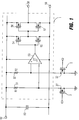
- FIGS 1 to 4 show circuit diagrams and a cross-section through a silicon wafer accommodating at least two insulated LDMOS level shift transistors and a floating well with circuitry.
- Such a device is constructed by means well known in the art and includes a substrate 7 of a first conductivity type, preferably with p polarity, a buried layer 8 with opposite conductivity, preferably with n+ polarity connected to an epitaxial layer, preferably of n- polarity. Above the buried layer 8, the epitaxial layer 6 is arranged.
- the regions 40 and 41 forming the body, 26 and 28 forming the source, and 27 forming the drain of the LDMOS transistor 3, and the regions 42 and 43 forming the body, 31 and 33 forming the source, and 32 forming the drain of the LDMOS transistor 5, as well as the p+ regions (p-iso regions) 12, 13, 14 and 15 separating the n-epitaxial layer 6 into isolated n-epitaxial regions 45, 46 and 47, are provided.
- the reference numerals 34 and 37 represent the gate electrodes.
- the p+ regions 13 and 14 isolate the LDMOS devices 3 and 5, respectively, from the floating-well circuitry.
- the N-MOS device formed inside P-well 10, and the P-MOS device formed inside N-well 11 form part of the circuitry inside floating well 1.
- the high voltage interconnect 2, 4 is made from the drain 27, 32 of the LDMOS transistor 3, 5 to the N-well portion 11 and the P-well portion 10 of the floating well, crossing over the LDMOS transistor 3, 5 and junction 35, 36.
- the circuit in the well floats from 0 volts up to 1000 V.
- Turn on/turn off signals are generated by a voltage drop V R1 , V R2 at the resistors R1 and R2 whereby V R1 , V R2 is 0 - 20 volts.
- the high voltage interconnects are necessary to connect the drain terminals of the LDMOS transistors to the resistors R1 and R2 in the floating well.
- a low voltage signal is provided to a level shifter which transfers it to a higher level.
- a voltage signal must be referenced to the output of an inverter stage. As this output voltages goes up and down, the signal applied floats with it.
- the n-epitaxial regions can be tied to a node having essentially a positive DC voltage with respect to the output of, for example, a half-bridge circuit, and supply a signal between the control-and reference-electrode of an NPN or N-channel FET (MOS-FET, IGBT) device having its reference electrode essentially connected to the output of said half-bridge circuit, via a high-voltage crossover and the circuitry in the floating well.
- MOS-FET, IGBT N-channel FET
- the term "reference electrode essentially connected to the output” is meant to cover a ripple on the DC voltate and an indirect connection of the reference electrode to the output of the half-bridge, eg.
- control electrode is meant to indicate a base and gate; and “reference electrode” indicates an emitter, source or cathode (N-channel).
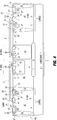
- Figs. 1 and 2 show circuit diagrams which illustrate the input/output electronics of the floating well.
- a bootstrap-capacitor 50 maintains a voltage between node 59 and 60 of typically between 5 and 20 Vdc; node 60 being positive with respect to node 59.
- the state of the voltage at node 58 with respect to node 59 can be changed in the following way: By applying a pulse of voltage of well controlled magnitude to the control electrode of level-shift transistor 3, this device will sink a pulse of current into its drain 27. This will result in a pulse-shaped voltage drop across resistor 51, relatively independent of the momentary voltage level of node 59 and 60. As there is no current flow through the other level-shift transistor 5 at that time, the voltage across resistor 52 will be essentially 0. As soon as the difference between the voltage across resistors 51 and 52 exceeds the hysteresis-level built into comparator 53, the output of comparator 53 will go high with respect to node 59. The non-inverting buffer formed by the transistors 54, 55, 56 and 57 will consequently pull output node 58 up to essentially the same voltage as node 60, thereby making node 58 positive with respect to node 59.
- a pulse of voltage of well controlled magnitude can be applied to the control electrode of transistor 5. This will result in a pulse-shaped flow of current into drain 32 of transistor 5, and consequently result in a voltage drop across resistor 52. As there is no flow of current into drain 27 of transistor 3, the voltage drop across resistor 51 will be 0. As soon as the difference between the voltages across resistors 51 and 52 exceeds the hysteresis-level built into comparator 53, the output of comparator 53 will go low with respect to node 59. The non-inverting buffer formed by the transistors 54, 55, 56 and 57 will consequently pull output node 58 down to essentially the same voltage as node 59.
- the circuit illustrated in Figure 2 acts in an identical fashion, with the pulsating current sources formed by transistors 3 and 5 being replaced by the cascoded current sources formed by transistor 63 and 64, or 65 and 66, respectively.
- Transistor 64 and 66 act as current sources, and can be standard N-MOS low-voltage devices or can even be replaced by low-voltage NPN bipolar devices.
- Transistors 63 and 65 are LDMOS devices, and are used to support the high voltage. Figure 2 shows two embodiments of these LDMOS devices; one with the body connected to the source (transistor 63) and one with the body connected to ground (transistor 65).
- An object of the present invention is to provide a circuit for a floating well and level shifter from ground potential to the floating well wherein high-voltage interconnect cross-overs and the problems associated therewith are substantially eliminated.
- Another object of the invention is to provide a device wherein there is a reduction of capacitances and chip size.
- a device wherein the level shift current sources are incorporated in the same N-well as the floating well circuitry, i.e. a built-in resistor is present in the n-epi layer.
- This built-in resistor with "parasitic" resistance may be used to convert the level shift signal current to a voltage signal that is sensed by circuitry in the floating well.
- the device of the invention lets current flow to the low voltage area through the gate-channel down to the ground and uses that current to generate a signal, i.e. the current flows from an n+ region through a n- epi resistor to a sense node.
- the structures of the invention are eminently suitable for eliminating problems associated with high-voltage interconnect crossovers discussed above and provides enhanced integrated circuit devices as further described and claimed hereinbelow.
- the invention further comprises improved and enhanced structures of the type just described but wherein the connection between the drain of the current sources and the floating well is spaced by a predetermined distance L1 and/or is spaced by a predetermined distance L1 over an area of reduced cross-section with a width W1, preferably a necked-in area, whereby the parasitic resistance between the current sources and the floating well is increased considerably.
- Such enhanced structures may embody circular LDMOS current sources of minimum dimensions thereby allowing the current sources to be located anywhere along the floating well including locations adjacent to or opposite the floating well.
- a sense resistor inside the floating well may be used which is voltage independent and by which the parasitic resistance is maximized.
- the parasitic resistor may be increased to a very high value and when so valued, the voltage independent sense resistor inside the floating well is used.
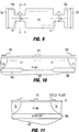
- the structure comprises two LDMOS level shift transistors 103, 105 comprising an epitaxial layer 106 of relatively high resistivity, (eg., a N-conductivity type layer) grown on a p- substrate 107 substantially as described above with respect to Figs. 1 to 4.
- an epitaxial layer 106 of relatively high resistivity eg., a N-conductivity type layer
- the drain 127, 132 of the level shift current sources formed by the LDMOS devices 103, 105 are spaced apart from the floating well 101 by a distance L1, and the high-voltage interconnect has been eliminated.
- the level shift current sources are placed in the same n-epitaxial region as the floating well circuitry, wherein the parasitic resistance R1, R2 between the drain n-region 119, 124 of the current sources and the n-regions 108, 182 and 183 is created and functionally utilized.
- the metal regions 127 and 132 form the drain of LDMOS 103 and 105 respectively.
- the n+ regions 119 and 124 form one of the terminals of the resistors R1 and R2 (151 and 152, 180 and 181), where the n+ regions 182 and 183, together with n-buried layer 108 form the other terminal of the resistors R1 and R2 (151 and 152, 180 and 181); these latter terminals are electrically equivalent to circuit-node 60.
- the resistance of R1 and R2 (151 and 152, 180 and 181) is formed by the part of the n-epitaxial layer 106 between region 119 and 108, 182 or between region 124 and 108, 183 respectively.
- a high-voltage structure which comprises a circuit 100 which comprises a floating well 101 connected to LDMOS level shift transistors 103 and 105 via R1 and R2 sense resistors 180 and 181 and in which high-voltage interconnects are eliminated although low voltage cross-overs 171 and 172 between the floating well and transistors for sensing purposes are retained. Since these are not of high voltage, the problems discussed above relative to high voltage cross-overs are eliminated. In this structure, all interconnects run above the silicon in a low voltage metal connection with less than 20V necessitating low voltage junctions.
- the invention also comprises several steps for increasing the parasitic resistance and increasing the flexibility of the layout of the resulting structures.
- one or both of the distances L1 and W1 between the current sources and the floating well are reduced and the cross-sectional areas 30, 31 of the interconnect regions are accordingly reduced.
- the interconnect regions are necked-in as illustrated in Fig. 9. This reduction in cross-sectional area has been found to increase the parasitic resistance between the current sources and the floating well considerably. This necking-in also considerably reduces the interference between the two HV-LDMOS structures, allowing them to be placed everywhere along the periphery of the floating well instead of opposite each other.
- the length of the drift region Ld is essentially the same as that for the floating well circuit.
- the oxide 9 underneath the metal 171 can support at least partially the voltage between metal and the p-iso 13, 14, p- buried 190 and p-substrate 107 portions of the device.
- This discovery makes it possible to reduce the drift region length Ld to that value that will support this lower voltage.
- the Ld length may be reduced from 50 ⁇ m to 25 ⁇ m resulting in a smaller cross-section of the n-epitaxial region.
- a field plate 192 is provided along the edge of the p-iso regions 13 and 14 for reducing the field strength.
- resistor As used herein is used in the broadest possible sense, i.e. these resistors can essentially be almost any circuit element or combination of elements having the property that a current through or change in current through the combination of these elements results in a voltage across or change in voltage across the combination of these circuit elements.
- resistor may be any essentially non-reactive circuit elements such as linear and non-linear resistors, transistors, diodes, etc.
Landscapes
- Engineering & Computer Science (AREA)
- Power Engineering (AREA)
- Physics & Mathematics (AREA)
- Condensed Matter Physics & Semiconductors (AREA)
- General Physics & Mathematics (AREA)
- Computer Hardware Design (AREA)
- Microelectronics & Electronic Packaging (AREA)
- Metal-Oxide And Bipolar Metal-Oxide Semiconductor Integrated Circuits (AREA)
- Insulated Gate Type Field-Effect Transistor (AREA)
Applications Claiming Priority (2)
| Application Number | Priority Date | Filing Date | Title |
|---|---|---|---|
| US971382 | 1992-11-04 | ||
| US07/971,382 US5446300A (en) | 1992-11-04 | 1992-11-04 | Semiconductor device configuration with multiple HV-LDMOS transistors and a floating well circuit |
Publications (3)
| Publication Number | Publication Date |
|---|---|
| EP0596565A2 true EP0596565A2 (de) | 1994-05-11 |
| EP0596565A3 EP0596565A3 (en) | 1997-06-04 |
| EP0596565B1 EP0596565B1 (de) | 2000-07-26 |
Family
ID=25518309
Family Applications (1)
| Application Number | Title | Priority Date | Filing Date |
|---|---|---|---|
| EP93203015A Expired - Lifetime EP0596565B1 (de) | 1992-11-04 | 1993-10-28 | Neue Anordnung für eine Vorrichtung mit vielen HV-LDMOS Transistoren und einer Schaltung innerhalb einer schwebenden Wanne |
Country Status (5)
| Country | Link |
|---|---|
| US (1) | US5446300A (de) |
| EP (1) | EP0596565B1 (de) |
| JP (1) | JPH06260601A (de) |
| DE (1) | DE69329097T2 (de) |
| TW (1) | TW244394B (de) |
Cited By (5)
| Publication number | Priority date | Publication date | Assignee | Title |
|---|---|---|---|---|
| EP0751572A2 (de) * | 1995-06-28 | 1997-01-02 | Fuji Electric Co. Ltd. | Integrierte Hochspannungsschaltung und Pegelverschiebungseinheit |
| EP0802568A1 (de) * | 1996-04-15 | 1997-10-22 | Mitsubishi Denki Kabushiki Kaisha | Halbleiteranordnung |
| EP0977264A1 (de) * | 1998-07-31 | 2000-02-02 | Motorola, Inc. | Halbleiterstruktur für Treiberschaltkreise mit Pegelverschiebung |
| DE19919130B4 (de) * | 1999-04-27 | 2005-10-06 | Infineon Technologies Ag | Monolithisch integrierte Halbleiteranordnung mit einem Steuerbereich und einem spannungsaufnehmenden Bereich |
| CN100514674C (zh) * | 2004-10-21 | 2009-07-15 | 株式会社瑞萨科技 | 半导体集成电路和半导体器件 |
Families Citing this family (14)
| Publication number | Priority date | Publication date | Assignee | Title |
|---|---|---|---|---|
| DE69207410T2 (de) * | 1992-09-18 | 1996-08-29 | Cons Ric Microelettronica | Monolithisch integrierte Brückenschaltung mit Transistoren und entsprechendes Herstellungsverfahren |
| JP4775357B2 (ja) * | 1995-04-12 | 2011-09-21 | 富士電機株式会社 | 高耐圧ic |
| JP4013785B2 (ja) * | 1995-04-12 | 2007-11-28 | 富士電機デバイステクノロジー株式会社 | 高耐圧ic |
| JP3565181B2 (ja) * | 1995-06-28 | 2004-09-15 | 富士電機デバイステクノロジー株式会社 | 高耐圧ic |
| DE69530216T2 (de) * | 1995-12-19 | 2004-02-12 | Consorzio Per La Ricerca Sulla Microelettronica Nel Mezzogiorno - Corimme | Monolithische Halbleiteranordnung mit Randstruktur und Verfahren zur Herstellung |
| US6184700B1 (en) | 1999-05-25 | 2001-02-06 | Lucent Technologies, Inc. | Fail safe buffer capable of operating with a mixed voltage core |
| JP4610786B2 (ja) * | 2001-02-20 | 2011-01-12 | 三菱電機株式会社 | 半導体装置 |
| DE10225860B4 (de) | 2001-06-11 | 2006-11-09 | Fuji Electric Co., Ltd., Kawasaki | Halbleiterbauteil |
| WO2007035862A2 (en) * | 2005-09-21 | 2007-03-29 | International Rectifier Corporation | Semiconductor package |
| KR101463076B1 (ko) * | 2008-03-28 | 2014-12-05 | 페어차일드코리아반도체 주식회사 | 레벨 시프트 소자들을 구비하는 고압 반도체소자 및 그의제조방법 |
| US8207580B2 (en) * | 2009-05-29 | 2012-06-26 | Power Integrations, Inc. | Power integrated circuit device with incorporated sense FET |
| TWI448055B (zh) | 2010-06-07 | 2014-08-01 | Richtek Technology Corp | 切換式電源供應器之控制電路及其控制方法以及用於其中之電晶體元件 |
| JP6379509B2 (ja) * | 2014-02-18 | 2018-08-29 | セイコーエプソン株式会社 | 回路装置及び電子機器 |
| TWI595653B (zh) * | 2016-09-13 | 2017-08-11 | 立積電子股份有限公司 | 用於增加信號振幅範圍的電晶體 |
Citations (4)
| Publication number | Priority date | Publication date | Assignee | Title |
|---|---|---|---|---|
| JPS6318660A (ja) * | 1986-07-11 | 1988-01-26 | Hitachi Micro Comput Eng Ltd | 半導体装置 |
| US4859878A (en) * | 1986-12-17 | 1989-08-22 | Nec Corporation | Bi-MOS levelshift circuit capable of controlling power consumption |
| EP0403449A2 (de) * | 1989-06-14 | 1990-12-19 | STMicroelectronics S.r.l. | Integrierte Vorrichtung mit komplementären LDMOS Leistungstransistoren, CMOS und vertikalen, integrierten PNP-Strukturen in Mischtechnologie, die imstande ist, relativ hohen Speisespannungen zu widerstehen |
| EP0514060A2 (de) * | 1991-05-06 | 1992-11-19 | SILICONIX Incorporated | DMOS-Transistorstruktur und Verfahren |
Family Cites Families (11)
| Publication number | Priority date | Publication date | Assignee | Title |
|---|---|---|---|---|
| FR1358573A (fr) * | 1963-03-06 | 1964-04-17 | Csf | Circuit électrique intégré |
| JPS58135666A (ja) * | 1983-01-14 | 1983-08-12 | Hitachi Ltd | 高耐圧半導体装置 |
| US4678936A (en) * | 1984-02-17 | 1987-07-07 | Analog Devices, Incorporated | MOS-cascoded bipolar current sources in non-epitaxial structure |
| US4661838A (en) * | 1985-10-24 | 1987-04-28 | General Electric Company | High voltage semiconductor devices electrically isolated from an integrated circuit substrate |
| IT1213027B (it) * | 1986-01-24 | 1989-12-07 | Sgs Microelettrica Spa | Densita'.!circuito integrato a semiconduttore, in particolare del tipo comprendente dispositivi ad alta tensione e dispositivi di elaborazione di segnale ad alta |
| IT1188465B (it) * | 1986-03-27 | 1988-01-14 | Sgs Microelettronica Spa | Rpocedimento per la fabbricazione di circuiti integrati a semiconduttore includenti dispositiv cmos e dispositivi elettronici ad alta tensione |
| JPH0812918B2 (ja) * | 1986-03-28 | 1996-02-07 | 株式会社東芝 | 半導体装置の製造方法 |
| EP0314465B1 (de) * | 1987-10-27 | 1998-05-06 | Nec Corporation | Halbleiteranordnung mit einem isolierten vertikalen Leistungs-MOSFET. |
| US5003362A (en) * | 1989-07-28 | 1991-03-26 | Dallas Semiconductor Corporation | Integrated circuit with high-impedance well tie |
| US5192989A (en) * | 1989-11-28 | 1993-03-09 | Nissan Motor Co., Ltd. | Lateral dmos fet device with reduced on resistance |
| US5146298A (en) * | 1991-08-16 | 1992-09-08 | Eklund Klas H | Device which functions as a lateral double-diffused insulated gate field effect transistor or as a bipolar transistor |
-
1992
- 1992-11-04 US US07/971,382 patent/US5446300A/en not_active Expired - Lifetime
-
1993
- 1993-10-28 EP EP93203015A patent/EP0596565B1/de not_active Expired - Lifetime
- 1993-10-28 DE DE69329097T patent/DE69329097T2/de not_active Expired - Fee Related
- 1993-11-04 JP JP5275531A patent/JPH06260601A/ja active Pending
- 1993-12-27 TW TW082111009A patent/TW244394B/zh active
Patent Citations (4)
| Publication number | Priority date | Publication date | Assignee | Title |
|---|---|---|---|---|
| JPS6318660A (ja) * | 1986-07-11 | 1988-01-26 | Hitachi Micro Comput Eng Ltd | 半導体装置 |
| US4859878A (en) * | 1986-12-17 | 1989-08-22 | Nec Corporation | Bi-MOS levelshift circuit capable of controlling power consumption |
| EP0403449A2 (de) * | 1989-06-14 | 1990-12-19 | STMicroelectronics S.r.l. | Integrierte Vorrichtung mit komplementären LDMOS Leistungstransistoren, CMOS und vertikalen, integrierten PNP-Strukturen in Mischtechnologie, die imstande ist, relativ hohen Speisespannungen zu widerstehen |
| EP0514060A2 (de) * | 1991-05-06 | 1992-11-19 | SILICONIX Incorporated | DMOS-Transistorstruktur und Verfahren |
Non-Patent Citations (2)
| Title |
|---|
| PATENT ABSTRACTS OF JAPAN vol. 012, no. 225 (E-626), 25 June 1988 & JP 63 018660 A (HITACHI MICRO COMPUT ENG LTD;OTHERS: 02), 26 January 1988, * |
| PROCEEDINGS OF THE INTERNATIONAL ELECTRON DEVICES MEETING, WASHINGTON, DEC. 8 - 11, 1991, no. -, 8 December 1991, INSTITUTE OF ELECTRICAL AND ELECTRONICS ENGINEERS, pages 91/145-148, XP000342114 MUKHERJEE S ET AL: "A HIGH CURRENT POWER IC TECHNOLOGY USING TRENCH DMOS POWER DEVICE" * |
Cited By (8)
| Publication number | Priority date | Publication date | Assignee | Title |
|---|---|---|---|---|
| EP0751572A2 (de) * | 1995-06-28 | 1997-01-02 | Fuji Electric Co. Ltd. | Integrierte Hochspannungsschaltung und Pegelverschiebungseinheit |
| EP0751572A3 (de) * | 1995-06-28 | 1999-11-24 | Fuji Electric Co. Ltd. | Integrierte Hochspannungsschaltung und Pegelverschiebungseinheit |
| EP0802568A1 (de) * | 1996-04-15 | 1997-10-22 | Mitsubishi Denki Kabushiki Kaisha | Halbleiteranordnung |
| US5894156A (en) * | 1996-04-15 | 1999-04-13 | Mitsubishi Denki Kabushiki Kaisha | Semiconductor device having a high breakdown voltage isolation region |
| EP0977264A1 (de) * | 1998-07-31 | 2000-02-02 | Motorola, Inc. | Halbleiterstruktur für Treiberschaltkreise mit Pegelverschiebung |
| US6097075A (en) * | 1998-07-31 | 2000-08-01 | Motorola, Inc. | Semiconductor structure for driver circuits with level shifting |
| DE19919130B4 (de) * | 1999-04-27 | 2005-10-06 | Infineon Technologies Ag | Monolithisch integrierte Halbleiteranordnung mit einem Steuerbereich und einem spannungsaufnehmenden Bereich |
| CN100514674C (zh) * | 2004-10-21 | 2009-07-15 | 株式会社瑞萨科技 | 半导体集成电路和半导体器件 |
Also Published As
| Publication number | Publication date |
|---|---|
| EP0596565A3 (en) | 1997-06-04 |
| TW244394B (de) | 1995-04-01 |
| JPH06260601A (ja) | 1994-09-16 |
| DE69329097D1 (de) | 2000-08-31 |
| US5446300A (en) | 1995-08-29 |
| EP0596565B1 (de) | 2000-07-26 |
| DE69329097T2 (de) | 2001-03-22 |
Similar Documents
| Publication | Publication Date | Title |
|---|---|---|
| EP0596565B1 (de) | Neue Anordnung für eine Vorrichtung mit vielen HV-LDMOS Transistoren und einer Schaltung innerhalb einer schwebenden Wanne | |
| US6130458A (en) | Power IC having SOI structure | |
| JP4037472B2 (ja) | グラウンドポテンシャルに接続されていないソース又はドレーンを有するHVp−チャンネル及びn−チャンネルデバイスを含む薄いエピタキシャルRESURF集積回路 | |
| US7704813B2 (en) | Reliable high-voltage junction field effect transistor and method of manufacturing therefor | |
| US8269305B2 (en) | High-voltage semiconductor device | |
| KR101157759B1 (ko) | 집적 레지스터를 가진 고전압 트랜지스터 장치 | |
| US9461115B2 (en) | Junction field effect transistor, integrated circuit for switching power supply, and switching power supply | |
| US6503782B2 (en) | Complementary accumulation-mode JFET integrated circuit topology using wide (>2eV) bandgap semiconductors | |
| US6853040B2 (en) | MOS transistor and fabrication method thereof | |
| KR20010015835A (ko) | 반도체 장치 | |
| US10679987B2 (en) | Bootstrap metal-oxide-semiconductor (MOS) device integrated with a high voltage MOS (HVMOS) device and a high voltage junction termination (HVJT) device | |
| TW201921588A (zh) | 整合高壓接面終端裝置與高壓金氧半導體裝置的積體電路及其製造方法 | |
| US5105251A (en) | Semiconductor device | |
| US7791139B2 (en) | Integrated circuit including a semiconductor assembly in thin-SOI technology | |
| KR970004363B1 (ko) | Da/ac 컨버터 | |
| US11056402B2 (en) | Integrated circuit chip and manufacturing method therefor, and gate drive circuit | |
| US5889310A (en) | Semiconductor device with high breakdown voltage island region | |
| US6355513B1 (en) | Asymmetric depletion region for normally off JFET | |
| US4969020A (en) | Semiconductor device | |
| JP2001507524A (ja) | ハーフブリッジ回路を具える半導体デバイス | |
| JP2007281196A (ja) | 半導体装置 | |
| WO2020230465A1 (ja) | 半導体集積回路 | |
| US5449936A (en) | High current MOS transistor bridge structure | |
| US6849491B2 (en) | Method of making high-voltage bipolar/CMOS/DMOS (BCD) devices | |
| EP0915517A2 (de) | Halbleitervorrichtung |
Legal Events
| Date | Code | Title | Description |
|---|---|---|---|
| PUAI | Public reference made under article 153(3) epc to a published international application that has entered the european phase |
Free format text: ORIGINAL CODE: 0009012 |
|
| AK | Designated contracting states |
Kind code of ref document: A2 Designated state(s): DE FR GB IT NL |
|
| RAP1 | Party data changed (applicant data changed or rights of an application transferred) |
Owner name: N.V. PHILIPS' GLOEILAMPENFABRIEKEN |
|
| PUAL | Search report despatched |
Free format text: ORIGINAL CODE: 0009013 |
|
| AK | Designated contracting states |
Kind code of ref document: A3 Designated state(s): DE FR GB IT NL |
|
| 17P | Request for examination filed |
Effective date: 19971204 |
|
| RAP3 | Party data changed (applicant data changed or rights of an application transferred) |
Owner name: KONINKLIJKE PHILIPS ELECTRONICS N.V. |
|
| GRAG | Despatch of communication of intention to grant |
Free format text: ORIGINAL CODE: EPIDOS AGRA |
|
| RTI1 | Title (correction) |
Free format text: NOVEL DEVICE CONFIGURATION WITH MULTIPLE HV-LDMOS TRANSISTORS AND A FLOATING WELL CIRCUIT |
|
| 17Q | First examination report despatched |
Effective date: 19990927 |
|
| GRAG | Despatch of communication of intention to grant |
Free format text: ORIGINAL CODE: EPIDOS AGRA |
|
| GRAH | Despatch of communication of intention to grant a patent |
Free format text: ORIGINAL CODE: EPIDOS IGRA |
|
| GRAH | Despatch of communication of intention to grant a patent |
Free format text: ORIGINAL CODE: EPIDOS IGRA |
|
| GRAA | (expected) grant |
Free format text: ORIGINAL CODE: 0009210 |
|
| AK | Designated contracting states |
Kind code of ref document: B1 Designated state(s): DE FR GB IT NL |
|
| PG25 | Lapsed in a contracting state [announced via postgrant information from national office to epo] |
Ref country code: NL Free format text: LAPSE BECAUSE OF FAILURE TO SUBMIT A TRANSLATION OF THE DESCRIPTION OR TO PAY THE FEE WITHIN THE PRESCRIBED TIME-LIMIT Effective date: 20000726 Ref country code: IT Free format text: LAPSE BECAUSE OF FAILURE TO SUBMIT A TRANSLATION OF THE DESCRIPTION OR TO PAY THE FEE WITHIN THE PRE;WARNING: LAPSES OF ITALIAN PATENTS WITH EFFECTIVE DATE BEFORE 2007 MAY HAVE OCCURRED AT ANY TIME BEFORE 2007. THE CORRECT EFFECTIVE DATE MAY BE DIFFERENT FROM THE ONE RECORDED.SCRIBED TIME-LIMIT Effective date: 20000726 |
|
| REF | Corresponds to: |
Ref document number: 69329097 Country of ref document: DE Date of ref document: 20000831 |
|
| ET | Fr: translation filed | ||
| NLV1 | Nl: lapsed or annulled due to failure to fulfill the requirements of art. 29p and 29m of the patents act | ||
| PLBE | No opposition filed within time limit |
Free format text: ORIGINAL CODE: 0009261 |
|
| STAA | Information on the status of an ep patent application or granted ep patent |
Free format text: STATUS: NO OPPOSITION FILED WITHIN TIME LIMIT |
|
| 26N | No opposition filed | ||
| REG | Reference to a national code |
Ref country code: GB Ref legal event code: IF02 |
|
| REG | Reference to a national code |
Ref country code: GB Ref legal event code: 746 Effective date: 20020911 |
|
| REG | Reference to a national code |
Ref country code: FR Ref legal event code: D6 |
|
| PGFP | Annual fee paid to national office [announced via postgrant information from national office to epo] |
Ref country code: DE Payment date: 20051213 Year of fee payment: 13 |
|
| PGFP | Annual fee paid to national office [announced via postgrant information from national office to epo] |
Ref country code: FR Payment date: 20061025 Year of fee payment: 14 |
|
| PGFP | Annual fee paid to national office [announced via postgrant information from national office to epo] |
Ref country code: GB Payment date: 20061030 Year of fee payment: 14 |
|
| PG25 | Lapsed in a contracting state [announced via postgrant information from national office to epo] |
Ref country code: DE Free format text: LAPSE BECAUSE OF NON-PAYMENT OF DUE FEES Effective date: 20070501 |
|
| GBPC | Gb: european patent ceased through non-payment of renewal fee |
Effective date: 20071028 |
|
| REG | Reference to a national code |
Ref country code: FR Ref legal event code: ST Effective date: 20080630 |
|
| PG25 | Lapsed in a contracting state [announced via postgrant information from national office to epo] |
Ref country code: GB Free format text: LAPSE BECAUSE OF NON-PAYMENT OF DUE FEES Effective date: 20071028 |
|
| PG25 | Lapsed in a contracting state [announced via postgrant information from national office to epo] |
Ref country code: FR Free format text: LAPSE BECAUSE OF NON-PAYMENT OF DUE FEES Effective date: 20071031 |