EP0403449A2 - Integrierte Vorrichtung mit komplementären LDMOS Leistungstransistoren, CMOS und vertikalen, integrierten PNP-Strukturen in Mischtechnologie, die imstande ist, relativ hohen Speisespannungen zu widerstehen - Google Patents
Integrierte Vorrichtung mit komplementären LDMOS Leistungstransistoren, CMOS und vertikalen, integrierten PNP-Strukturen in Mischtechnologie, die imstande ist, relativ hohen Speisespannungen zu widerstehen Download PDFInfo
- Publication number
- EP0403449A2 EP0403449A2 EP90830268A EP90830268A EP0403449A2 EP 0403449 A2 EP0403449 A2 EP 0403449A2 EP 90830268 A EP90830268 A EP 90830268A EP 90830268 A EP90830268 A EP 90830268A EP 0403449 A2 EP0403449 A2 EP 0403449A2
- Authority
- EP
- European Patent Office
- Prior art keywords
- transistor
- channel
- ldmos
- structures
- cmos
- Prior art date
- Legal status (The legal status is an assumption and is not a legal conclusion. Google has not performed a legal analysis and makes no representation as to the accuracy of the status listed.)
- Granted
Links
Images
Classifications
-
- H—ELECTRICITY
- H10—SEMICONDUCTOR DEVICES; ELECTRIC SOLID-STATE DEVICES NOT OTHERWISE PROVIDED FOR
- H10D—INORGANIC ELECTRIC SEMICONDUCTOR DEVICES
- H10D84/00—Integrated devices formed in or on semiconductor substrates that comprise only semiconducting layers, e.g. on Si wafers or on GaAs-on-Si wafers
- H10D84/80—Integrated devices formed in or on semiconductor substrates that comprise only semiconducting layers, e.g. on Si wafers or on GaAs-on-Si wafers characterised by the integration of at least one component covered by groups H10D12/00 or H10D30/00, e.g. integration of IGFETs
- H10D84/82—Integrated devices formed in or on semiconductor substrates that comprise only semiconducting layers, e.g. on Si wafers or on GaAs-on-Si wafers characterised by the integration of at least one component covered by groups H10D12/00 or H10D30/00, e.g. integration of IGFETs of only field-effect components
- H10D84/83—Integrated devices formed in or on semiconductor substrates that comprise only semiconducting layers, e.g. on Si wafers or on GaAs-on-Si wafers characterised by the integration of at least one component covered by groups H10D12/00 or H10D30/00, e.g. integration of IGFETs of only field-effect components of only insulated-gate FETs [IGFET]
- H10D84/85—Complementary IGFETs, e.g. CMOS
- H10D84/856—Complementary IGFETs, e.g. CMOS the complementary IGFETs having different architectures than each other, e.g. high-voltage and low-voltage CMOS
-
- H—ELECTRICITY
- H10—SEMICONDUCTOR DEVICES; ELECTRIC SOLID-STATE DEVICES NOT OTHERWISE PROVIDED FOR
- H10D—INORGANIC ELECTRIC SEMICONDUCTOR DEVICES
- H10D84/00—Integrated devices formed in or on semiconductor substrates that comprise only semiconducting layers, e.g. on Si wafers or on GaAs-on-Si wafers
- H10D84/40—Integrated devices formed in or on semiconductor substrates that comprise only semiconducting layers, e.g. on Si wafers or on GaAs-on-Si wafers characterised by the integration of at least one component covered by groups H10D12/00 or H10D30/00 with at least one component covered by groups H10D10/00 or H10D18/00, e.g. integration of IGFETs with BJTs
- H10D84/401—Combinations of FETs or IGBTs with BJTs
Definitions
- the present invention relates to a mixed technology, "smart power", integrated device containing power transistors and control logic and analog driving circuitry combined in a monolithic silicon chip.
- the power transistor e.g. VDMOS
- the driving circuitry for power transistors operate at about 12V, while in order to ensure a driving level on the gate of a VDMOS power transistor of 10V and if a reasonable process "spread" is accounted for, the supply voltage of CMOS transistors of the relative driving circuit should be at least 15V.
- better operating conditions of a VDMOS power transistor i.e. a lower resistance R on
- R on the driving voltage level on the gate may be raised to 15-20V, as it is well known to a skilled technician.
- CMOS transistors having an operating voltage of about 20V in a monolithically integrated semiconductor device of the "smart power" type in order to drive directly the output power transistors with a relatively high voltage without employing special level shifter circuits.
- the present invention has the main objective of providing, in a monolithically integrated "smart power" type device, CMOS structures and isolated collector, vertical, PNP transistors capable of withstanding a higher operating voltage than the voltage normally withstood by these devices, when they are formed monolith strictlyically together in a single chip.
- the device is characterized by the fact that it comprises regions of phosphorus doped, n-type silicon of similar diffusion profile extending from the surface of the n-type epitaxial layer wherein the different devices are formed, respectively, through the drain area of n-channel LDMOS transistors extending between the gate electrode thereof and the adjacent isolating field oxide, the body area of p-channel LDMOS transistors, extending between the gate electrode thereof and the adjacent isolation field oxide, the drain area of n-channel MOS transistors, extending between the gate electrode thereof and the adjacent isolation field oxide, and the emitter area of isolated collector vertical PNP bipolar transistors, and by a depth sufficient to contain, respectively, the n+ doped drain region of n-channel LDMOS transistors, the p+ doped source region of p-channel LDMOS transistors, the n+ doped drain region of n-channel MOS transistors and the p+ doped emitter region of the PNP transistors.
- the same auxiliary n ⁇ doped region may conveniently constitute a body region which is so formed without other specific additional process steps.
- CMOS structures formed by pairs of complementary LDMOS transistors when provided with such an n-doped region by phosphorus implantation, become capable of operating with a supply voltage of about 20V without requiring special precautions, such as "field plates", thus remaining advantageously compact.
- the n-doped region obtained by phosphorus implantation in the drain area of the transistor, reduces the sensitivity to electrical stresses due to hot electrons, by acting as a "drain extension" region; this permits to the transistor to withstand a supply voltage of about 12V.
- the additional n-doped region obtained by phosphorus implantation through the emitter area of the transistor permits to improve the transistor's performance transistors by increasing the charge in the base region of the transistor and to increase the "punchthrough" voltage between emitter and collector.
- CMOS structures and vertical PNP transistors to withstand a specifically increased operating voltage specifically increased permits to build mixed technology integrated circuits (i.e. "smart power" devices) with far less pronounced interfacing problems among the different types of circuits, with enhanced possibilities of fully exploiting the intrinsic peculiarities of the different devices and with a higher degree of reliability.
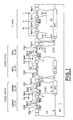
- FIG. 1 An hypothetical partial cross section of an integrated "smart power" type integrated device, wherein it is relatively easy to put in evidence, though in a schematic way, the aspects of the invention, is shown in Fig. 1.
- the depicted cross section does not include VDMOS power transistors, which may be easily imagined present in a different zone of the integrated device from the zone shown in the partial cross section of the figure, wherein two different CMOS structures are depicted, a first structure formed by an n-channel and a p-channel LDMOS transistor and a second structure formed by a p-channel and by an n-channel MOS transistor, and the structure of an isolated collector, vertical PNP bipolar transistor.
- the device comprises a p-type silicon substrate 1 on which an epitaxial n-type silicon layer 2 has been grown after doping with arsenic and/or with boron certain areas defined on the surface of the monocrystalline silicon substrate 1 in order to form the n+ buried layers 3 and the p-type bottom isolations 4.
- the integrated device further comprises an isolation structure among the different integrated devices which, in the depicted example, is formed by a field oxide layer 5 grown on the surface of the silicon 2, after doping with boron predifined areas on the silicon surface in order to form, in accordance with well known techniques, the p-well regions 6 (i.e. top isolations and p-well) as well as regions with a heavier boron doping charge 11, also known as p-field region, while growing the field oxide 5, according to a known technique.
- gate structures 12 commonly of doped polycrystalline silicon, are formed.
- the n-channel, LDMOS transistor comprises a p-body region 7, produced in the silicon by implanting boron under self-alignment conditions in the source area extending between the gate 12 and the field oxide 9 and by successively diffusing the implanted boron until obtaining the desired diffusion profile of the region 7, the n+ source and drain junctions 10 and the p+ region 9 having a relatively high doping level formed in the source region for contacting the body region 7.
- a p-channel LDMOS transistor comprises a p-doped region 7 (having substantially the same profile of the n-channel LDMOS body region), formed in the drain region of the transistor, the p+ drain and source junctions 9 and the n+ region 10, formed in the source area in order to contact an n-body region, the formation of which together with other n-regions in the different integrated structures according to the present invention will be described later.
- the p-channel MOS transistor forming the second CMOS structure depicted in Fig. 1 comprises, as usual, the source and drain p+ junctions 9 and a "back gate” contact, n+ region 10, formed in the source zone of the transistor.
- the n-channel MOS transistor comprises the n+ source and drain junctions 10 and a "back gate” contact, p+ region 9, formed in the source zone of the transistor.
- the structure of the isolated collector PNP vertical transistor comprises the collector (C) and emitter (E) contact p+ diffusions 9 and the base (B) n+ contact diffusion 10.
- an n-type region 8 extends from the surface of the epitaxial layer respectively in the drain area of the n-channel LDMOS transistor extending between the gate electrode and the isolation field oxide, in the source area of the p-channel LDMOS transistor extending between the gate electrode and the isolation field oxide, in the drain area of the n-channel MOS transistor extending between the gate electrode and the adjacent isolation field oxide and in the emitter area of the isolated collector PNP bipolar transistor defined by the surrounding isolation field oxide, for a depth sufficient to contain at least, respectively, the n+ drain junction of the n-channel LDMOS transistor, the p+ source junctions and n+ body contact regions of the p-channel LDMOS transistor, the n+ drain junction of the n-channel MOS transistor and the n+ emitter junction of the PNP transistor.
- n-type regions 8 are made evident in the schematic cross section depicted in Fig. 1 by means of a thick line.
- the distinct regions 8 may be easily formed simultaneously in the indicated zones without requiring critical process steps by simply implanting phosphorus under self-alignment conditions in the indicated areas and by diffusing the implanted phosphorus before proceeding to the formation of the heavily doped n+ regions obtained by implanting arsenic and diffusing it and of the heavily doped p+ regions obtained by implanting boron and diffusing it, which are contained within said auxiliary regions 8.
- the doping level of this additional n-region 8 may be comprised between 1013 and 1014 (phosphorus) atoms per cubic centimeter.
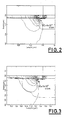
- Fig. 2 Shown in Fig. 2 are the equimodal electric field lines in the overlapping region between the drain and the gate of an n-channel LDMOS transistor having a 600 Angstroms ( ⁇ ) thick gate oxide, produced by means of computer model simulation for the case of a transistor without the auxiliary n-doped region (8 of Fig. 1) in accordance with the present invention and subjected to a 20V bias.
- the maximum electric field intensity is evaluated to be 6 x 10⁵ V/cm.
- Fig. 3 shown in Fig. 3 are the equimodal electric field lines in the same overlapping region under identical bias conditions (20V) of the example shown in Fig. 2, but wherein the n-channel LDMOS transistor is provided with the auxiliary n-region, doped with phosphorus at 1014 atoms per cubic centimeter, in accordance with the present invention.
- the equimodal electric field lines are more "distended" than those of Fig. 1 and the maximum field electric intensity may be evaluated to be 5 x 10⁵ V/cm. This is 17% less than the maximum intensity evaluated in the case of the transistor of the prior art without the auxialiary phosphorus doped region.
- CMOS structure formed by the complementary LDMOS transistors provided with the n-doped region 8 (Fig. 1) in accordance with the present invention may funtions with a supply voltage of 20 V and it may be directly interfaced, as a driving device, with VDMOS power transistors for example, thus eliminating the need for adequate level shifting circuits.
- an LDMOS transistor structure modified ac cording to the invention is intrinsically capable of withstanding voltages in the order of 20V without requiring the formation of "field plates" (according to a known technique for increasing the intrinsic breakdown voltage of integrated transistors) which inevitably clashes with compactness requirements of these integrated structures.
- the complementary LDMOS transistors depicted as forming a CMOS structure in Fig. 1, may themselves be employed as power transistors through an appropriate layout configuration, exploiting also for such applications, the same improved performance in terms of voltage withstanding ability and reduced resistance (R on ), derived by the presence of said additional n-region 8, in accordance with the present invention.
- the electrical performances of the other CMOS structure shown, formed by the pair of complementary MOS transistors, are improved because the n-region 8 formed in the drain region of the n-channel transistor acts as a drain extension region thus increasing the nominal operating voltage of the relative CMOS structure.
- Another, non-negligeable advantage is obtained also in terms of improved performance of the isolated collector, vertical PNP bipolar transistor by providing also this integrated device with the n-region 8 doped with phosphorus enchroaching in the base region of the transistor.
- the consequent increase of the doping level of the base region reduces sensitivity to depletion of the base region thus increasing the punchthrough voltage between emitter and collector.
Landscapes
- Metal-Oxide And Bipolar Metal-Oxide Semiconductor Integrated Circuits (AREA)
- Bipolar Transistors (AREA)
- Insulated Gate Type Field-Effect Transistor (AREA)
Applications Claiming Priority (2)
| Application Number | Priority Date | Filing Date | Title |
|---|---|---|---|
| IT8983626A IT1235843B (it) | 1989-06-14 | 1989-06-14 | Dispositivo integrato contenente strutture di potenza formate con transistori ldmos complementari, strutture cmos e pnp verticali con aumentata capacita' di supportare un'alta tensione di alimentazione. |
| IT8362689 | 1989-06-14 |
Publications (3)
| Publication Number | Publication Date |
|---|---|
| EP0403449A2 true EP0403449A2 (de) | 1990-12-19 |
| EP0403449A3 EP0403449A3 (de) | 1992-07-08 |
| EP0403449B1 EP0403449B1 (de) | 1996-09-04 |
Family
ID=11323341
Family Applications (1)
| Application Number | Title | Priority Date | Filing Date |
|---|---|---|---|
| EP90830268A Expired - Lifetime EP0403449B1 (de) | 1989-06-14 | 1990-06-14 | Integrierte Vorrichtung mit komplementären LDMOS Leistungstransistoren, CMOS und vertikalen, integrierten PNP-Strukturen in Mischtechnologie, die imstande ist, relativ hohen Speisespannungen zu widerstehen |
Country Status (5)
| Country | Link |
|---|---|
| US (1) | US5041895A (de) |
| EP (1) | EP0403449B1 (de) |
| JP (1) | JP3043367B2 (de) |
| DE (1) | DE69028354T2 (de) |
| IT (1) | IT1235843B (de) |
Cited By (10)
| Publication number | Priority date | Publication date | Assignee | Title |
|---|---|---|---|---|
| FR2675311A1 (fr) * | 1991-04-09 | 1992-10-16 | Samsung Electronics Co Ltd | Dispositif semi-conducteur du type bicmos pour circuits integres et son procede de fabrication. |
| EP0522579A3 (en) * | 1991-07-12 | 1994-07-20 | Texas Instruments Inc | Level-shifter circuit for integrated circuits |
| EP0658938A1 (de) * | 1993-12-15 | 1995-06-21 | STMicroelectronics S.r.l. | Integrierte Schaltung die eine EPROM-Zelle und einen MOS-Transistor enthält |
| EP0677876A1 (de) * | 1994-04-08 | 1995-10-18 | Texas Instruments Incorporated | Hoch- und Niederspannungs-CMOS-Bauteil und Herstellungsverfahren |
| EP0596565A3 (en) * | 1992-11-04 | 1997-06-04 | Koninkl Philips Electronics Nv | Novel device configuration with multiple hv-ldmos transistors and a floating well circuit. |
| EP0802567A3 (de) * | 1996-04-15 | 2000-07-05 | Denso Corporation | Halbleiteranordnung und Verfahren zu ihrer Herstellung |
| US6242787B1 (en) | 1995-11-15 | 2001-06-05 | Denso Corporation | Semiconductor device and manufacturing method thereof |
| EP0809294B1 (de) * | 1996-05-21 | 2002-01-02 | Co.Ri.M.Me. Consorzio Per La Ricerca Sulla Microelettronica Nel Mezzogiorno | Leistungshalbleiterbauelementstruktur mit vertikalem PNP-Transistor |
| US6831331B2 (en) | 1995-11-15 | 2004-12-14 | Denso Corporation | Power MOS transistor for absorbing surge current |
| CN102176467A (zh) * | 2011-03-29 | 2011-09-07 | 上海宏力半导体制造有限公司 | 沟槽式金属氧化物半导体场效应晶体管 |
Families Citing this family (34)
| Publication number | Priority date | Publication date | Assignee | Title |
|---|---|---|---|---|
| US5465189A (en) * | 1990-03-05 | 1995-11-07 | Texas Instruments Incorporated | Low voltage triggering semiconductor controlled rectifiers |
| US5204541A (en) * | 1991-06-28 | 1993-04-20 | Texas Instruments Incorporated | Gated thyristor and process for its simultaneous fabrication with high- and low-voltage semiconductor devices |
| JP3218642B2 (ja) * | 1991-09-27 | 2001-10-15 | 富士電機株式会社 | 大電流集積回路の配線構造 |
| US5225702A (en) * | 1991-12-05 | 1993-07-06 | Texas Instruments Incorporated | Silicon controlled rectifier structure for electrostatic discharge protection |
| EP0657995B1 (de) | 1993-12-07 | 1999-10-13 | STMicroelectronics S.r.l. | Ausgangstufe mit Transistoren von unterschiedlichem Typ |
| JP3335060B2 (ja) * | 1995-02-21 | 2002-10-15 | シャープ株式会社 | 半導体装置の製造方法 |
| JP3400181B2 (ja) * | 1995-04-25 | 2003-04-28 | ローム株式会社 | 半導体装置およびその製造方法 |
| DE19548060A1 (de) * | 1995-12-21 | 1997-06-26 | Siemens Ag | Durch Feldeffekt steuerbares Leistungs-Halbleiterbauelement mit Temperatursensor |
| US5950091A (en) * | 1996-12-06 | 1999-09-07 | Advanced Micro Devices, Inc. | Method of making a polysilicon gate conductor of an integrated circuit formed as a sidewall spacer on a sacrificial material |
| US6124174A (en) * | 1997-05-16 | 2000-09-26 | Advanced Micro Devices, Inc. | Spacer structure as transistor gate |
| US5866934A (en) * | 1997-06-20 | 1999-02-02 | Advanced Micro Devices, Inc. | Parallel and series-coupled transistors having gate conductors formed on sidewall surfaces of a sacrificial structure |
| TW421874B (en) * | 1998-01-09 | 2001-02-11 | Winbond Electronics Corp | Integrated structure for output buffer and silicon controlled rectifier |
| US6897525B1 (en) * | 1998-11-26 | 2005-05-24 | Sanyo Electric Co., Ltd. | Semiconductor device and method of manufacturing the same |
| JP3317345B2 (ja) * | 1999-07-23 | 2002-08-26 | 日本電気株式会社 | 半導体装置 |
| US6818494B1 (en) * | 2001-03-26 | 2004-11-16 | Hewlett-Packard Development Company, L.P. | LDMOS and CMOS integrated circuit and method of making |
| JP4689861B2 (ja) * | 2001-04-03 | 2011-05-25 | レンゴー株式会社 | カートン |
| JP4660004B2 (ja) * | 2001-04-13 | 2011-03-30 | 三洋電機株式会社 | Mos半導体装置の製造方法 |
| JP2003017577A (ja) * | 2001-07-04 | 2003-01-17 | Denso Corp | 半導体装置 |
| US6768183B2 (en) * | 2001-04-20 | 2004-07-27 | Denso Corporation | Semiconductor device having bipolar transistors |
| JP4003438B2 (ja) * | 2001-11-07 | 2007-11-07 | 株式会社デンソー | 半導体装置の製造方法および半導体装置 |
| JP3970689B2 (ja) * | 2002-05-30 | 2007-09-05 | エルピーダメモリ株式会社 | 半導体装置及びその製造方法 |
| US7825488B2 (en) | 2006-05-31 | 2010-11-02 | Advanced Analogic Technologies, Inc. | Isolation structures for integrated circuits and modular methods of forming the same |
| US6855985B2 (en) * | 2002-09-29 | 2005-02-15 | Advanced Analogic Technologies, Inc. | Modular bipolar-CMOS-DMOS analog integrated circuit & power transistor technology |
| US7019377B2 (en) * | 2002-12-17 | 2006-03-28 | Micrel, Inc. | Integrated circuit including high voltage devices and low voltage devices |
| SE0303106D0 (sv) * | 2003-11-21 | 2003-11-21 | Infineon Technologies Ag | Ldmos transistor device, integrated circuit, and fabrication method thereof |
| US7230302B2 (en) * | 2004-01-29 | 2007-06-12 | Enpirion, Inc. | Laterally diffused metal oxide semiconductor device and method of forming the same |
| JP4795869B2 (ja) * | 2006-06-26 | 2011-10-19 | レンゴー株式会社 | 包装体 |
| US7781843B1 (en) | 2007-01-11 | 2010-08-24 | Hewlett-Packard Development Company, L.P. | Integrating high-voltage CMOS devices with low-voltage CMOS |
| US20090127629A1 (en) * | 2007-11-15 | 2009-05-21 | Zia Alan Shafi | Method of forming npn and pnp bipolar transistors in a CMOS process flow that allows the collectors of the bipolar transistors to be biased differently than the substrate material |
| US7906810B2 (en) * | 2008-08-06 | 2011-03-15 | United Microelectronics Corp. | LDMOS device for ESD protection circuit |
| KR101681494B1 (ko) * | 2010-03-03 | 2016-12-01 | 삼성전자 주식회사 | 반도체 장치 |
| US9214457B2 (en) | 2011-09-20 | 2015-12-15 | Alpha & Omega Semiconductor Incorporated | Method of integrating high voltage devices |
| US9356512B2 (en) * | 2013-07-29 | 2016-05-31 | Broadcom Corporation | Envelope tracking power supply with direct connection to power source |
| GB2561388B (en) | 2017-04-13 | 2019-11-06 | Raytheon Systems Ltd | Silicon carbide integrated circuit |
Family Cites Families (7)
| Publication number | Priority date | Publication date | Assignee | Title |
|---|---|---|---|---|
| US4120707A (en) * | 1977-03-30 | 1978-10-17 | Harris Corporation | Process of fabricating junction isolated IGFET and bipolar transistor integrated circuit by diffusion |
| FR2571178B1 (fr) * | 1984-09-28 | 1986-11-21 | Thomson Csf | Structure de circuit integre comportant des transistors cmos a tenue en tension elevee, et son procede de fabrication |
| JPS61166071A (ja) * | 1985-01-17 | 1986-07-26 | Toshiba Corp | 半導体装置及びその製造方法 |
| JPS62119936A (ja) * | 1985-11-19 | 1987-06-01 | Fujitsu Ltd | コンプリメンタリ−lsiチツプ |
| GB2186117B (en) * | 1986-01-30 | 1989-11-01 | Sgs Microelettronica Spa | Monolithically integrated semiconductor device containing bipolar junction,cmosand dmos transistors and low leakage diodes and a method for its fabrication |
| JPH01272145A (ja) * | 1988-04-25 | 1989-10-31 | Hitachi Ltd | 半導体集積回路装置及びその製造方法 |
| US4918026A (en) * | 1989-03-17 | 1990-04-17 | Delco Electronics Corporation | Process for forming vertical bipolar transistors and high voltage CMOS in a single integrated circuit chip |
-
1989
- 1989-06-14 IT IT8983626A patent/IT1235843B/it active
-
1990
- 1990-06-08 US US07/535,774 patent/US5041895A/en not_active Ceased
- 1990-06-14 DE DE69028354T patent/DE69028354T2/de not_active Expired - Fee Related
- 1990-06-14 JP JP2156586A patent/JP3043367B2/ja not_active Expired - Fee Related
- 1990-06-14 EP EP90830268A patent/EP0403449B1/de not_active Expired - Lifetime
Cited By (17)
| Publication number | Priority date | Publication date | Assignee | Title |
|---|---|---|---|---|
| FR2675311A1 (fr) * | 1991-04-09 | 1992-10-16 | Samsung Electronics Co Ltd | Dispositif semi-conducteur du type bicmos pour circuits integres et son procede de fabrication. |
| EP0522579A3 (en) * | 1991-07-12 | 1994-07-20 | Texas Instruments Inc | Level-shifter circuit for integrated circuits |
| EP0596565A3 (en) * | 1992-11-04 | 1997-06-04 | Koninkl Philips Electronics Nv | Novel device configuration with multiple hv-ldmos transistors and a floating well circuit. |
| US5610421A (en) * | 1993-12-15 | 1997-03-11 | Sgs-Thomson Microelectronics S.R.L. | Integrated circuit with EPROM cells |
| EP0658938A1 (de) * | 1993-12-15 | 1995-06-21 | STMicroelectronics S.r.l. | Integrierte Schaltung die eine EPROM-Zelle und einen MOS-Transistor enthält |
| US5837554A (en) * | 1993-12-15 | 1998-11-17 | Sgs-Thomson Microelectronics S.R.L. | Integrated circuit with EPROM cells |
| US5747850A (en) * | 1994-04-08 | 1998-05-05 | Texas Instruments Incorporated | Extended drain resurf lateral DMOS devices |
| US5501994A (en) * | 1994-04-08 | 1996-03-26 | Texas Instruments Incorporated | Extended drain resurf lateral DMOS devices |
| US5498554A (en) * | 1994-04-08 | 1996-03-12 | Texas Instruments Incorporated | Method of making extended drain resurf lateral DMOS devices |
| EP0677876A1 (de) * | 1994-04-08 | 1995-10-18 | Texas Instruments Incorporated | Hoch- und Niederspannungs-CMOS-Bauteil und Herstellungsverfahren |
| US6242787B1 (en) | 1995-11-15 | 2001-06-05 | Denso Corporation | Semiconductor device and manufacturing method thereof |
| US6831331B2 (en) | 1995-11-15 | 2004-12-14 | Denso Corporation | Power MOS transistor for absorbing surge current |
| EP0802567A3 (de) * | 1996-04-15 | 2000-07-05 | Denso Corporation | Halbleiteranordnung und Verfahren zu ihrer Herstellung |
| EP0809294B1 (de) * | 1996-05-21 | 2002-01-02 | Co.Ri.M.Me. Consorzio Per La Ricerca Sulla Microelettronica Nel Mezzogiorno | Leistungshalbleiterbauelementstruktur mit vertikalem PNP-Transistor |
| US6518139B1 (en) | 1996-05-21 | 2003-02-11 | Co.Ri.M.Me Consorzio Per La Sulla Microelectronica Nel Mezzogiorno | Power semiconductor device structure with vertical PNP transistor |
| CN102176467A (zh) * | 2011-03-29 | 2011-09-07 | 上海宏力半导体制造有限公司 | 沟槽式金属氧化物半导体场效应晶体管 |
| CN102176467B (zh) * | 2011-03-29 | 2016-03-23 | 上海华虹宏力半导体制造有限公司 | 沟槽式金属氧化物半导体场效应晶体管 |
Also Published As
| Publication number | Publication date |
|---|---|
| US5041895A (en) | 1991-08-20 |
| DE69028354D1 (de) | 1996-10-10 |
| JP3043367B2 (ja) | 2000-05-22 |
| IT1235843B (it) | 1992-11-03 |
| JPH0324758A (ja) | 1991-02-01 |
| IT8983626A0 (it) | 1989-06-14 |
| DE69028354T2 (de) | 1997-01-23 |
| EP0403449B1 (de) | 1996-09-04 |
| EP0403449A3 (de) | 1992-07-08 |
Similar Documents
| Publication | Publication Date | Title |
|---|---|---|
| EP0403449A2 (de) | Integrierte Vorrichtung mit komplementären LDMOS Leistungstransistoren, CMOS und vertikalen, integrierten PNP-Strukturen in Mischtechnologie, die imstande ist, relativ hohen Speisespannungen zu widerstehen | |
| US4862233A (en) | Integrated circuit device having vertical MOS provided with Zener diode | |
| US7279399B2 (en) | Method of forming isolated pocket in a semiconductor substrate | |
| US5218228A (en) | High voltage MOS transistors with reduced parasitic current gain | |
| US5602416A (en) | Power integrated circuit ("PIC") structure | |
| US5394007A (en) | Isolated well and method of making | |
| US5087579A (en) | Method for fabricating an integrated bipolar-CMOS circuit isolation for providing different backgate and substrate bias | |
| US5132235A (en) | Method for fabricating a high voltage MOS transistor | |
| US4035826A (en) | Reduction of parasitic bipolar effects in integrated circuits employing insulated gate field effect transistors via the use of low resistance substrate contacts extending through source region | |
| US5912495A (en) | High voltage driver circuit with diode | |
| JP2718907B2 (ja) | Pic構造体及びその製造方法 | |
| USRE37424E1 (en) | Mixed technology integrated device comprising complementary LDMOS power transistors, CMOS and vertical PNP integrated structures having an enhanced ability to withstand a relatively high supply voltage | |
| US6831346B1 (en) | Buried layer substrate isolation in integrated circuits | |
| US5786622A (en) | Bipolar transistor with a ring emitter | |
| JPH0348458A (ja) | Bi―CMOS集積回路およびその製造方法 | |
| JPH0821679B2 (ja) | 半導体装置 | |
| EP0792514B1 (de) | Herstellungsverfahren eines integrierten schaltkreises mit komplementären isolierten bipolartransistoren | |
| KR0169965B1 (ko) | 보조 ldmos 전력트랜지스터 cmos 및 수직 pnp 집적구조포함의 모놀리식 집적회로 | |
| US6030888A (en) | Method of fabricating high-voltage junction-isolated semiconductor devices | |
| US4656498A (en) | Oxide-isolated integrated Schottky logic | |
| JPH05226588A (ja) | 半導体装置およびその製造方法 | |
| JPH0637264A (ja) | 半導体装置 |
Legal Events
| Date | Code | Title | Description |
|---|---|---|---|
| PUAI | Public reference made under article 153(3) epc to a published international application that has entered the european phase |
Free format text: ORIGINAL CODE: 0009012 |
|
| AK | Designated contracting states |
Kind code of ref document: A2 Designated state(s): DE FR GB NL SE |
|
| PUAL | Search report despatched |
Free format text: ORIGINAL CODE: 0009013 |
|
| AK | Designated contracting states |
Kind code of ref document: A3 Designated state(s): DE FR GB NL SE |
|
| 17P | Request for examination filed |
Effective date: 19921217 |
|
| 17Q | First examination report despatched |
Effective date: 19940913 |
|
| GRAH | Despatch of communication of intention to grant a patent |
Free format text: ORIGINAL CODE: EPIDOS IGRA |
|
| GRAH | Despatch of communication of intention to grant a patent |
Free format text: ORIGINAL CODE: EPIDOS IGRA |
|
| GRAA | (expected) grant |
Free format text: ORIGINAL CODE: 0009210 |
|
| AK | Designated contracting states |
Kind code of ref document: B1 Designated state(s): DE FR GB NL SE |
|
| REF | Corresponds to: |
Ref document number: 69028354 Country of ref document: DE Date of ref document: 19961010 |
|
| ET | Fr: translation filed | ||
| PLBE | No opposition filed within time limit |
Free format text: ORIGINAL CODE: 0009261 |
|
| STAA | Information on the status of an ep patent application or granted ep patent |
Free format text: STATUS: NO OPPOSITION FILED WITHIN TIME LIMIT |
|
| 26N | No opposition filed | ||
| REG | Reference to a national code |
Ref country code: FR Ref legal event code: D6 |
|
| PGFP | Annual fee paid to national office [announced via postgrant information from national office to epo] |
Ref country code: SE Payment date: 20010417 Year of fee payment: 12 |
|
| REG | Reference to a national code |
Ref country code: GB Ref legal event code: IF02 |
|
| PGFP | Annual fee paid to national office [announced via postgrant information from national office to epo] |
Ref country code: FR Payment date: 20020610 Year of fee payment: 13 |
|
| PGFP | Annual fee paid to national office [announced via postgrant information from national office to epo] |
Ref country code: GB Payment date: 20020612 Year of fee payment: 13 |
|
| PG25 | Lapsed in a contracting state [announced via postgrant information from national office to epo] |
Ref country code: SE Free format text: LAPSE BECAUSE OF NON-PAYMENT OF DUE FEES Effective date: 20020615 |
|
| PGFP | Annual fee paid to national office [announced via postgrant information from national office to epo] |
Ref country code: DE Payment date: 20020619 Year of fee payment: 13 |
|
| EUG | Se: european patent has lapsed | ||
| PG25 | Lapsed in a contracting state [announced via postgrant information from national office to epo] |
Ref country code: GB Free format text: LAPSE BECAUSE OF NON-PAYMENT OF DUE FEES Effective date: 20030614 |
|
| PG25 | Lapsed in a contracting state [announced via postgrant information from national office to epo] |
Ref country code: DE Free format text: LAPSE BECAUSE OF NON-PAYMENT OF DUE FEES Effective date: 20040101 |
|
| GBPC | Gb: european patent ceased through non-payment of renewal fee |
Effective date: 20030614 |
|
| PG25 | Lapsed in a contracting state [announced via postgrant information from national office to epo] |
Ref country code: FR Free format text: LAPSE BECAUSE OF NON-PAYMENT OF DUE FEES Effective date: 20040227 |
|
| REG | Reference to a national code |
Ref country code: FR Ref legal event code: ST |
|
| PGFP | Annual fee paid to national office [announced via postgrant information from national office to epo] |
Ref country code: NL Payment date: 20040603 Year of fee payment: 15 |
|
| PG25 | Lapsed in a contracting state [announced via postgrant information from national office to epo] |
Ref country code: NL Free format text: LAPSE BECAUSE OF NON-PAYMENT OF DUE FEES Effective date: 20060101 |
|
| NLV4 | Nl: lapsed or anulled due to non-payment of the annual fee |
Effective date: 20060101 |