EP0591084A2 - Structure de surface latérale de rainure - Google Patents
Structure de surface latérale de rainure Download PDFInfo
- Publication number
- EP0591084A2 EP0591084A2 EP93480127A EP93480127A EP0591084A2 EP 0591084 A2 EP0591084 A2 EP 0591084A2 EP 93480127 A EP93480127 A EP 93480127A EP 93480127 A EP93480127 A EP 93480127A EP 0591084 A2 EP0591084 A2 EP 0591084A2
- Authority
- EP
- European Patent Office
- Prior art keywords
- trench
- layer
- polysilicon
- storage node
- doped polysilicon
- Prior art date
- Legal status (The legal status is an assumption and is not a legal conclusion. Google has not performed a legal analysis and makes no representation as to the accuracy of the status listed.)
- Withdrawn
Links
Images


Classifications
-
- H—ELECTRICITY
- H10—SEMICONDUCTOR DEVICES; ELECTRIC SOLID-STATE DEVICES NOT OTHERWISE PROVIDED FOR
- H10D—INORGANIC ELECTRIC SEMICONDUCTOR DEVICES
- H10D1/00—Resistors, capacitors or inductors
- H10D1/60—Capacitors
- H10D1/62—Capacitors having potential barriers
- H10D1/66—Conductor-insulator-semiconductor capacitors, e.g. MOS capacitors
- H10D1/665—Trench conductor-insulator-semiconductor capacitors, e.g. trench MOS capacitors
-
- Y—GENERAL TAGGING OF NEW TECHNOLOGICAL DEVELOPMENTS; GENERAL TAGGING OF CROSS-SECTIONAL TECHNOLOGIES SPANNING OVER SEVERAL SECTIONS OF THE IPC; TECHNICAL SUBJECTS COVERED BY FORMER USPC CROSS-REFERENCE ART COLLECTIONS [XRACs] AND DIGESTS
- Y10—TECHNICAL SUBJECTS COVERED BY FORMER USPC
- Y10S—TECHNICAL SUBJECTS COVERED BY FORMER USPC CROSS-REFERENCE ART COLLECTIONS [XRACs] AND DIGESTS
- Y10S257/00—Active solid-state devices, e.g. transistors, solid-state diodes
- Y10S257/915—Active solid-state devices, e.g. transistors, solid-state diodes with titanium nitride portion or region
-
- Y—GENERAL TAGGING OF NEW TECHNOLOGICAL DEVELOPMENTS; GENERAL TAGGING OF CROSS-SECTIONAL TECHNOLOGIES SPANNING OVER SEVERAL SECTIONS OF THE IPC; TECHNICAL SUBJECTS COVERED BY FORMER USPC CROSS-REFERENCE ART COLLECTIONS [XRACs] AND DIGESTS
- Y10—TECHNICAL SUBJECTS COVERED BY FORMER USPC
- Y10S—TECHNICAL SUBJECTS COVERED BY FORMER USPC CROSS-REFERENCE ART COLLECTIONS [XRACs] AND DIGESTS
- Y10S257/00—Active solid-state devices, e.g. transistors, solid-state diodes
- Y10S257/924—Active solid-state devices, e.g. transistors, solid-state diodes with passive device, e.g. capacitor, or battery, as integral part of housing or housing element, e.g. cap
Definitions
- This invention relates to a trench sidewall structure. More specifically, the invention relates to a sidewall structure which comprises an oxide collar layer, a doped polysilicon layer, and a diffusion barrier layer.
- the trench sidewall structure reduces trench sidewall leakage between the storage node poly and the oxide collar.
- parasitic sidewall leakage through the trench sidewalls is due to the formation of a parasitic sidewall transistor as explained in a paper by N.C.C. Lu et al., IEEE J. Solid-State Circuits SC-21: 627 (1986).
- the parasitic MOS transistor causes a leakage current to pass through a sidewall portion of a channel formed adjacent to the trench. Such leakage can occur from bitline contact to the storage node, and from storage node to the substrate, for example.
- One way to reduce this parasitic sidewall leakage is to increase the thickness of the oxide collar normally placed around the trench near the top of the trench (the trench neck).
- collar thickness is increased at the expense of storage node thickness within the trench, the size of the trench opening being fixed.
- increasing the collar thickness (1) reduces the contact area available for contact with the storage node, (2) increases the RC time constant of the storage node poly, and (3) introduces other process constraints.
- DRAM dynamic memory
- the present invention is directed to a trench sidewall structure which reduces leakage through the trench sidewall.
- the trench sidewall structure disclosed herein is a viable alternative to reduce the parasitic sidewall leakage for the present and future DRAMs.
- the invention provides a heavily doped polysilicon layer and a diffusion barrier layer placed between the storage node poly of a trench and the oxide collar of the trench.
- the heavily doped polysilicon layer has the same polarity as the array well into which the trench is placed.
- the DRAM cell is placed in a well near the surface of the substrate.
- the polarity of the array well doping is opposite to that of the substrate. For example, consider an n+ substrate with a p-well. If the trench array is placed in a p-well, a p+ polysilicon layer is placed between the storage node poly (generally n+ polysilicon with an n+ substrate) and the oxide collar (for example, tetraethylorthosilicate [TEOS!
- a diffusion barrier layer is also added, which makes ohmic contact with the p+ polysilicon layer as well as the n+ polysilicon in the storage node, to prevent the formation of a p-n junction.
- the diffusion barrier layer comprises titanium nitride.
- tantalum nitride is another material having similar diffusion barrier properties.
- this trench sidewall structure is to shift the threshold voltage by 1.1 V and thereby reduce the subthreshold leakage through the trench sidewall. This is in addition to the effect of the oxide collar in reducing leakage.
- leakage current may be reduced without increasing the thickness of the oxide collar.
- the oxide collar thickness may be reduced while keeping the same leakage, if the trench sidewall structure of the subject invention is utilized.
- the trench structure is formed by initially etching a trench. This is done by anisotropically etching the silicon substrate to the required trench depth using an oxide or silicon nitride mask.
- a capacitor insulator is formed, and the trench is filled with polysilicon, planarized, and recessed to a depth more than the well.
- an n+ substrate, a p-well, and an n+ poly fill is utilized.
- a thin layer of TEOS for the oxide collar is then deposited followed by a thin p+ polysilicon layer.
- the polysilicon and the TEOS are then anisotropically etched to form spacers.
- a thin layer of titanium nitride is then deposited followed by n+ polysilicon deposition.
- the n+ polysilicon is then planarized and recessed, and the exposed titanium nitride is etched off. Further conventional processing is then used to form the desired cell structure which incorporates the trench having the sidewalls as provided herein.
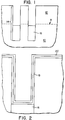
- the trench sidewall structure comprises an oxide collar layer 18, adjacent a doped polysilicon layer 20, adjacent a diffusion barrier layer 26.
- the doped polysilicon layer 20 and the diffusion barrier layer 26 separate the oxide collar layer 18 from the trench storage node polysilicon 28.
- This sidewall structure helps to reduce leakage through the well adjacent to the trench sidewall, for example from the storage node polysilicon 28 to substrate 10.
- FIG. 1 an n+ semiconductor substrate 10 having a p-well 12 formed therein is shown.
- a trench 14 has been formed in the substrate 10 and partially in the p-well 12.
- the polysilicon fill 16 is recessed to a level below the well 12. 8 shows the end of the well.
- an oxide collar layer 18 is conformally deposited into the trench, over which a further layer of doped polysilicon 20 is conformally deposited adjacent to the oxide collar layer 18.
- the oxide collar layer 18 and doped polysilicon layer 20 are then anisotropically etched to remove these layers from the bottom surface 22 of the trench adjacent the polysilicon 16 fill (see FIG. 3). By utilizing anisotropic etching, the oxide collar layer 18 and the doped polysilicon layer 20 remain on the vertical sidewalls 24 of the trench.
- a diffusion barrier layer 26 is then conformally deposited, such that it is adjacent to the bottom surface 22 and the doped polysilicon 20.
- the trench is then filled, for example with n+ polysilicon, to form the storage node 28 as shown in FIG. 5.
- the storage node 28 is planarized and recessed, after which the exposed diffusion barrier layer 26 is etched off (see FIG. 6). This leaves a trench structure comprising the storage node 28 surrounded by the trench sidewall structure of oxide collar 18, doped polysilicon 20, and diffusion barrier layer 26. Further processing according to known techniques can then be utilized to form various cell structures utilizing the trench structure. Such a structure is useful whenever trench sidewall leakage is a problem and the reduction of such leakage can be provided by the subject invention.
- the trench sidewall structure is utilized in a p-well array on an n+ substrate, with a trench having an n+ polysilicon storage node.
- a TEOS oxide collar is provided, adjacent a p+ doped polysilicon layer, adjacent a titanium nitride diffusion barrier layer.
- This structure effectively reduces trench sidewall leakage, for example from the trench storage node to the substrate through the well adjacent to the oxide collar.
- Other combinations are also possible.
- an n-well array over a p+ substrate with p+ storage node polysilicon inside can be utilized.
- an n+ polysilicon layer is placed between the oxide collar and the titanium nitride diffusion barrier.
- suitable materials for the oxide collar such as silicon nitride or other forms of oxide, may be used.
- suitable materials for the diffusion barrier layer are tantalum nitride, for example.
- the p+ doped polysilicon layer has the same polarity as the array well. Therefore, if the trench is placed in an n+ well, an n+ doped polysilicon layer would be placed between the storage node poly and the oxide collar.
- etching and deposition techniques known in the art can be utilized to form the various layers of the trench sidewall structure.
- deposition of the oxide collar and the doped polysilicon layers, as well as the diffusion barrier layer should be by a method which results in a conformally deposited layer, such as chemical vapor deposition.
- Sputtering techniques or plasma deposition could also be utilized as long as conformal deposition is attainable.
- the anisotropic etch can utilize suitable etchants, which depend upon the material being etched.
- an anisotropic etch of p+ doped polysilicon may be performed by reactive ion etching using bromine or chlorine based chemistry.
- the anisotropic etch of the oxide layer is done by reactive ion etching using fluorine based chemistry. Reactive ion etching using chlorine based chemistry may be used to etch titanium nitride.
- the etching of tantalum nitride is similar to that of titanium nitride.
- the resulting sidewall structure of the preferred embodiment is placed inside a trench of opening dimensions about 0.5 microns, and has a diffusion barrier layer of a thickness of about 10 nm, a doped polysilicon layer of a thickness of about 100 nm, and an oxide collar layer of a thickness of about 25 nm.
- These layer thicknesses can be altered depending upon the reduction in leakage desired.
- the subthreshold leakage is reduced by a voltage bias of 1.1 V (bandgap). It is also possible to reduce the oxide collar thickness, if desirable, while still maintaining the same sidewall leakage as the thicker oxide collar provided, if the sidewall structure of the invention is utilized.
Landscapes
- Semiconductor Memories (AREA)
- Element Separation (AREA)
- Semiconductor Integrated Circuits (AREA)
Applications Claiming Priority (2)
| Application Number | Priority Date | Filing Date | Title |
|---|---|---|---|
| US956125 | 1992-10-02 | ||
| US07/956,125 US5283453A (en) | 1992-10-02 | 1992-10-02 | Trench sidewall structure |
Publications (2)
| Publication Number | Publication Date |
|---|---|
| EP0591084A2 true EP0591084A2 (fr) | 1994-04-06 |
| EP0591084A3 EP0591084A3 (fr) | 1994-12-07 |
Family
ID=25497779
Family Applications (1)
| Application Number | Title | Priority Date | Filing Date |
|---|---|---|---|
| EP19930480127 Withdrawn EP0591084A3 (fr) | 1992-10-02 | 1993-09-10 | Structure de surface latérale de rainure. |
Country Status (3)
| Country | Link |
|---|---|
| US (2) | US5283453A (fr) |
| EP (1) | EP0591084A3 (fr) |
| JP (1) | JP2620499B2 (fr) |
Cited By (1)
| Publication number | Priority date | Publication date | Assignee | Title |
|---|---|---|---|---|
| EP0794576A3 (fr) * | 1996-03-04 | 2004-01-07 | Siemens Aktiengesellschaft | Condensateur silloné à DRAM avec anneau d'isolation |
Families Citing this family (33)
| Publication number | Priority date | Publication date | Assignee | Title |
|---|---|---|---|---|
| US5451809A (en) * | 1994-09-07 | 1995-09-19 | Kabushiki Kaisha Toshiba | Smooth surface doped silicon film formation |
| US5593912A (en) * | 1994-10-06 | 1997-01-14 | International Business Machines Corporation | SOI trench DRAM cell for 256 MB DRAM and beyond |
| US6207494B1 (en) * | 1994-12-29 | 2001-03-27 | Infineon Technologies Corporation | Isolation collar nitride liner for DRAM process improvement |
| US5618751A (en) * | 1996-05-23 | 1997-04-08 | International Business Machines Corporation | Method of making single-step trenches using resist fill and recess |
| DE19621855C2 (de) * | 1996-05-31 | 2003-03-27 | Univ Dresden Tech | Verfahren zur Herstellung von Metallisierungen auf Halbleiterkörpern unter Verwendung eines gepulsten Vakuumbogenverdampfers |
| US6232233B1 (en) * | 1997-09-30 | 2001-05-15 | Siemens Aktiengesellschaft | Methods for performing planarization and recess etches and apparatus therefor |
| US5963814A (en) * | 1997-10-28 | 1999-10-05 | Micron Technology, Inc. | Method of forming recessed container cells by wet etching conductive layer and dissimilar layer formed over conductive layer |
| US6583457B1 (en) * | 1997-10-28 | 2003-06-24 | Micron Technology, Inc. | Recessed container cells and method of forming the same |
| US6057216A (en) * | 1997-12-09 | 2000-05-02 | International Business Machines Corporation | Low temperature diffusion process for dopant concentration enhancement |
| US6190955B1 (en) | 1998-01-27 | 2001-02-20 | International Business Machines Corporation | Fabrication of trench capacitors using disposable hard mask |
| US6066566A (en) * | 1998-01-28 | 2000-05-23 | International Business Machines Corporation | High selectivity collar oxide etch processes |
| EP0981164A3 (fr) | 1998-08-18 | 2003-10-15 | International Business Machines Corporation | Remplissage à faible resistance pour condensateur à sillon profond |
| GB2341483B (en) * | 1998-09-11 | 2003-10-01 | Siemens Plc | Improved process for dram cell production |
| US6194736B1 (en) | 1998-12-17 | 2001-02-27 | International Business Machines Corporation | Quantum conductive recrystallization barrier layers |
| US6541371B1 (en) | 1999-02-08 | 2003-04-01 | Novellus Systems, Inc. | Apparatus and method for depositing superior Ta(N)/copper thin films for barrier and seed applications in semiconductor processing |
| US6259129B1 (en) | 1999-04-20 | 2001-07-10 | International Business Machines Corporation | Strap with intrinsically conductive barrier |
| US6236077B1 (en) | 1999-04-20 | 2001-05-22 | International Business Machines Corporation | Trench electrode with intermediate conductive barrier layer |
| US6693320B1 (en) | 1999-08-30 | 2004-02-17 | Micron Technology, Inc. | Capacitor structures with recessed hemispherical grain silicon |
| US6326277B1 (en) | 1999-08-30 | 2001-12-04 | Micron Technology, Inc. | Methods of forming recessed hemispherical grain silicon capacitor structures |
| US6303424B1 (en) * | 1999-10-21 | 2001-10-16 | United Microelectronics Corp. | Method for fabricating a buried bit line in a DRAM cell |
| DE19956078B4 (de) * | 1999-11-22 | 2006-12-28 | Infineon Technologies Ag | Verfahren zur Herstellung eines Isolationskragens in einem Grabenkondensators |
| JP4497260B2 (ja) * | 2000-08-31 | 2010-07-07 | エルピーダメモリ株式会社 | 半導体集積回路装置およびその製造方法 |
| US6503845B1 (en) * | 2001-05-01 | 2003-01-07 | Applied Materials Inc. | Method of etching a tantalum nitride layer in a high density plasma |
| KR100417211B1 (ko) * | 2001-12-20 | 2004-02-05 | 동부전자 주식회사 | 반도체 소자의 금속 배선 형성 방법 |
| DE10328634B3 (de) * | 2003-06-26 | 2004-10-21 | Infineon Technologies Ag | Verfahren zur Herstellung eines Buried-Strap-Kontakts für einen Speicherkondensator |
| US6953724B2 (en) * | 2003-09-25 | 2005-10-11 | International Business Machines Corporation | Self-limited metal recess for deep trench metal fill |
| TWI229414B (en) * | 2003-10-03 | 2005-03-11 | Promos Technologies Inc | Method of fabricating deep trench capacitor |
| US7754601B2 (en) * | 2008-06-03 | 2010-07-13 | Taiwan Semiconductor Manufacturing Co., Ltd. | Semiconductor interconnect air gap formation process |
| KR101608902B1 (ko) * | 2009-11-12 | 2016-04-05 | 삼성전자주식회사 | 소자 분리 구조물을 갖는 반도체 소자 |
| US8642423B2 (en) * | 2011-11-30 | 2014-02-04 | International Business Machines Corporation | Polysilicon/metal contact resistance in deep trench |
| US9881870B2 (en) * | 2015-12-30 | 2018-01-30 | Taiwan Semiconductor Manufacturing Co., Ltd. | Semiconductor device and manufacturing method thereof |
| US9960118B2 (en) | 2016-01-20 | 2018-05-01 | Globalfoundries Inc. | Contact using multilayer liner |
| CN109326596B (zh) * | 2017-08-01 | 2022-05-03 | 联华电子股份有限公司 | 具有电容连接垫的半导体结构与电容连接垫的制作方法 |
Family Cites Families (19)
| Publication number | Priority date | Publication date | Assignee | Title |
|---|---|---|---|---|
| US4605947A (en) * | 1983-03-07 | 1986-08-12 | Motorola Inc. | Titanium nitride MOS device gate electrode and method of producing |
| JPS6072261A (ja) * | 1983-09-28 | 1985-04-24 | Fujitsu Ltd | 半導体装置 |
| US4914739A (en) * | 1984-10-31 | 1990-04-03 | Texas Instruments, Incorporated | Structure for contacting devices in three dimensional circuitry |
| US4621414A (en) * | 1985-03-04 | 1986-11-11 | Advanced Micro Devices, Inc. | Method of making an isolation slot for integrated circuit structure |
| US4689871A (en) * | 1985-09-24 | 1987-09-01 | Texas Instruments Incorporated | Method of forming vertically integrated current source |
| EP0236089B1 (fr) * | 1986-03-03 | 1992-08-05 | Fujitsu Limited | Mémoire dynamique à accès aléatoire comprenant un condensateur dans un sillon |
| US4785337A (en) * | 1986-10-17 | 1988-11-15 | International Business Machines Corporation | Dynamic ram cell having shared trench storage capacitor with sidewall-defined bridge contacts and gate electrodes |
| US4918502A (en) * | 1986-11-28 | 1990-04-17 | Hitachi, Ltd. | Semiconductor memory having trench capacitor formed with sheath electrode |
| JPS63193562A (ja) * | 1987-02-06 | 1988-08-10 | Toshiba Corp | バイポ−ラトランジスタの製造方法 |
| US4783248A (en) * | 1987-02-10 | 1988-11-08 | Siemens Aktiengesellschaft | Method for the production of a titanium/titanium nitride double layer |
| JP2807226B2 (ja) * | 1987-09-12 | 1998-10-08 | ソニー株式会社 | 半導体装置の製造方法 |
| JPH01120050A (ja) * | 1987-11-02 | 1989-05-12 | Hitachi Ltd | 半導体記憶装置 |
| JPH01222469A (ja) * | 1988-03-01 | 1989-09-05 | Fujitsu Ltd | 半導体記憶装置とその製造方法 |
| US4914740A (en) * | 1988-03-07 | 1990-04-03 | International Business Corporation | Charge amplifying trench memory cell |
| JPH01227468A (ja) * | 1988-03-08 | 1989-09-11 | Oki Electric Ind Co Ltd | 半導体記憶装置 |
| JPH0770617B2 (ja) * | 1989-05-15 | 1995-07-31 | 株式会社東芝 | 半導体記憶装置 |
| US5021849A (en) * | 1989-10-30 | 1991-06-04 | Motorola, Inc. | Compact SRAM cell with polycrystalline silicon diode load |
| US5164333A (en) * | 1990-06-19 | 1992-11-17 | Siemens Aktiengesellschaft | Method for manufacturing a multi-layer gate electrode for a mos transistor |
| JPH0449654A (ja) * | 1990-06-19 | 1992-02-19 | Nec Corp | 半導体メモリ |
-
1992
- 1992-10-02 US US07/956,125 patent/US5283453A/en not_active Expired - Fee Related
-
1993
- 1993-09-03 JP JP5219471A patent/JP2620499B2/ja not_active Expired - Lifetime
- 1993-09-10 EP EP19930480127 patent/EP0591084A3/fr not_active Withdrawn
- 1993-12-10 US US08/166,306 patent/US5521114A/en not_active Expired - Fee Related
Cited By (1)
| Publication number | Priority date | Publication date | Assignee | Title |
|---|---|---|---|---|
| EP0794576A3 (fr) * | 1996-03-04 | 2004-01-07 | Siemens Aktiengesellschaft | Condensateur silloné à DRAM avec anneau d'isolation |
Also Published As
| Publication number | Publication date |
|---|---|
| US5283453A (en) | 1994-02-01 |
| US5521114A (en) | 1996-05-28 |
| EP0591084A3 (fr) | 1994-12-07 |
| JPH06196552A (ja) | 1994-07-15 |
| JP2620499B2 (ja) | 1997-06-11 |
Similar Documents
| Publication | Publication Date | Title |
|---|---|---|
| US5521114A (en) | Trench sidewall structure | |
| US6008104A (en) | Method of fabricating a trench capacitor with a deposited isolation collar | |
| US7429507B2 (en) | Semiconductor device having both memory and logic circuit and its manufacture | |
| US6806137B2 (en) | Trench buried bit line memory devices and methods thereof | |
| US7445987B2 (en) | Offset vertical device | |
| US6204140B1 (en) | Dynamic random access memory | |
| US6509599B1 (en) | Trench capacitor with insulation collar and method for producing the trench capacitor | |
| EP0967644A2 (fr) | Condensateur ensillonné pour DRAM | |
| EP0967653A2 (fr) | Condensateur semi-conducteur à sillon de type DRAM | |
| US6437401B1 (en) | Structure and method for improved isolation in trench storage cells | |
| EP0703625A2 (fr) | Procédé de DRAM à sillon profond sur SOI pour cellule DRAM à faible courant | |
| US6255684B1 (en) | DRAM cell configuration and method for its production | |
| US6605838B1 (en) | Process flow for thick isolation collar with reduced length | |
| US6100131A (en) | Method of fabricating a random access memory cell | |
| US7223669B2 (en) | Structure and method for collar self-aligned to buried plate | |
| US6853025B2 (en) | Trench capacitor with buried strap | |
| US6373086B1 (en) | Notched collar isolation for suppression of vertical parasitic MOSFET and the method of preparing the same | |
| US7030442B2 (en) | Stack-film trench capacitor and method for manufacturing the same | |
| US5512768A (en) | Capacitor for use in DRAM cell using surface oxidized silicon nodules | |
| US6404000B1 (en) | Pedestal collar structure for higher charge retention time in trench-type DRAM cells | |
| US6583462B1 (en) | Vertical DRAM having metallic node conductor | |
| HK1024338A (en) | Dram trench capacitor | |
| HK1024562A (en) | Semiconductor dram trench capacitor | |
| HK1020111A (en) | A trench capacitor with isolation collar | |
| HK1015532A (en) | Isolation structure for dram cell with trench capacitor |
Legal Events
| Date | Code | Title | Description |
|---|---|---|---|
| PUAI | Public reference made under article 153(3) epc to a published international application that has entered the european phase |
Free format text: ORIGINAL CODE: 0009012 |
|
| AK | Designated contracting states |
Kind code of ref document: A2 Designated state(s): DE FR GB |
|
| PUAL | Search report despatched |
Free format text: ORIGINAL CODE: 0009013 |
|
| AK | Designated contracting states |
Kind code of ref document: A3 Designated state(s): DE FR GB |
|
| STAA | Information on the status of an ep patent application or granted ep patent |
Free format text: STATUS: THE APPLICATION IS DEEMED TO BE WITHDRAWN |
|
| 18D | Application deemed to be withdrawn |
Effective date: 19950608 |