EP0588191B1 - Austausch von Daten- und Taktleitungen auf mehrformatigen Datenbussen - Google Patents
Austausch von Daten- und Taktleitungen auf mehrformatigen Datenbussen Download PDFInfo
- Publication number
- EP0588191B1 EP0588191B1 EP93114208A EP93114208A EP0588191B1 EP 0588191 B1 EP0588191 B1 EP 0588191B1 EP 93114208 A EP93114208 A EP 93114208A EP 93114208 A EP93114208 A EP 93114208A EP 0588191 B1 EP0588191 B1 EP 0588191B1
- Authority
- EP
- European Patent Office
- Prior art keywords
- data
- bus
- signal
- clock
- iic
- Prior art date
- Legal status (The legal status is an assumption and is not a legal conclusion. Google has not performed a legal analysis and makes no representation as to the accuracy of the status listed.)
- Expired - Lifetime
Links
Images


Classifications
-
- G—PHYSICS
- G06—COMPUTING OR CALCULATING; COUNTING
- G06F—ELECTRIC DIGITAL DATA PROCESSING
- G06F13/00—Interconnection of, or transfer of information or other signals between, memories, input/output devices or central processing units
- G06F13/38—Information transfer, e.g. on bus
-
- G—PHYSICS
- G06—COMPUTING OR CALCULATING; COUNTING
- G06F—ELECTRIC DIGITAL DATA PROCESSING
- G06F13/00—Interconnection of, or transfer of information or other signals between, memories, input/output devices or central processing units
- G06F13/38—Information transfer, e.g. on bus
- G06F13/42—Bus transfer protocol, e.g. handshake; Synchronisation
- G06F13/4282—Bus transfer protocol, e.g. handshake; Synchronisation on a serial bus, e.g. I2C bus, SPI bus
- G06F13/4291—Bus transfer protocol, e.g. handshake; Synchronisation on a serial bus, e.g. I2C bus, SPI bus using a clocked protocol
Definitions
- the present invention relates to bus-controlled signal processing systems.
- Signal processing systems may be implemented using a variety of integrated circuits controlled by one or more control microcomputers ( ⁇ C). Communications between the various functions typically involves a data bus such as a serial data bus.
- ⁇ C control microcomputers
- Communications between the various functions typically involves a data bus such as a serial data bus.
- IC signal processing integrated circuits
- manufacturers support several different communications protocols. For example, Philips and ITT support bus standards designated the Inter IC (IIC or I2C), and Intermetall (IM) standards, respectively.
- Bus standards specify signal patterns that indicate message start and end conditions, device address, and message data for devices coupled to the bus. For example, a particular transition occurring on one signal during a particular state on another signal indicates "start of message" for the IIC bus standard. Signal waveforms that are generated to conform to IM bus standard may inadvertently create the "start message" condition for the IIC bus. If both IM and IIC devices are connected to a bus, an IIC device may be activated unintentionally during an IM format message. As a result, two devices attempt to communicate simultaneously on the bus. Corruption of any transmission that is in progress and incorrect system operation may result.
- bus conflicts will depend on data values and timing. Thus, the conflicts and any subsequent system malfunctions will be intermittent. Testing of the system may identify data patterns that should be avoided to prevent bus conflicts. However, exhaustive and lengthy testing of all possible data patterns may be required to ensure reliable system performance. In addition, it would be necessary to repeat the testing when a device type is changed or a new device is added to the bus.
- An aspect of the invention involves a data bus having first and second bus lines for coupling first and second data processing devices to a control device.
- the first data processing device has clock and data terminals that are coupled to the first and second bus lines, respectively.
- the second data processing device has clock and data terminals that are coupled to the second and first bus lines, respectively.
- the control device generates clock and data signals on the first and second bus lines, respectively, during a first mode of operation to control the operation of the first data processing device without affecting the operation of the second data processing device.
- the control device generates clock and data signals on the second and first bus lines, respectively, during a second mode of operation to control the operation of the second data processing device without affecting the operation of the first data processing device.
- Figure 1 shows a portion of a bus-controlled signal processing system including control microcomputer ( ⁇ C) 100 and devices 150 and 160.
- a serial data bus comprising signals SERBUS1, SERBUS2, and SERBUS3 couples ⁇ C 100 to devices 150 and 160.
- Control ⁇ C 100 may be a microprocessor such as the MC68HC05 from Motorola.
- Devices 150 and 160 represent one or more types of signal or data processing devices that may be digital or analog integrated circuits (IC's). The operation of these devices is controlled via the serial data bus using the Inter IC (IIC) bus protocol for device 150 and the Intermetall (IM) bus protocol for device 160.
- IIC Inter IC
- IM Intermetall
- device 150 represents IC's such as Microchip 24C02 (EEPROM), Motorola MC44802 (tuning processor), and Philips 8444 (digital-to-analog converter (DAC)).
- device 160 represents IC's such as the Thomson 1A68109 ( Proscan processor), Thomson 1A68106 (stereo processor), and Thomson 1A68105 (picture-in-picture (PIP) processor).
- FIG. 2 illustrates the bus signal format for both the IIC and IM bus protocols.
- communications in IIC format requires signal SCL, a clock signal, and signal SDA, a data signal.
- signals SCL and SDA should be at logic 1.
- a "message start” condition occurs when signal SDA goes to logic 0 during the time that signal SCL is at logic 1.
- the start condition is followed by a "start bit”, an 8-bit device address, and an acknowledge bit that is used to acknowledge receipt of the address.
- the address acknowledge bit is followed by 8 bits (one byte) of data and data acknowledge bit.
- the address and data in IIC format is transmitted most significant bit (MSB) first.
- MSB most significant bit
- EOT end of transmission
- the IM bus protocol shown in Figure 2B requires three signals designated IDENT, an enable signal, CLOCK, and DATA.
- a "message start” is indicated by a transition on signal IDENT to logic 0 followed by a transition on signal CLOCK to a logic 0.
- "Message start” is followed by an 8-bit address and 8 bits of data.
- the address and data in IM format is transmitted least significant bit (LSB) first.
- Signal IDENT changes to logic 1 after all address bits are transmitted to cause each IM device that is attached to the bus to compare the transmitted address to the device address. No acknowledge bits are included. Additional bytes of data may follow the initial byte.
- "Message stop” or EOT is indicated by a pulse on signal IDENT.
- signals IDENT, CLOCK, and DATA of IM bus protocol IC's such as device 160 in Figure 1 are coupled to signals SERBUS3, SERBUS1, and SERBUS2, respectively, from ⁇ C 100 in Figure 1.
- signals SERBUS1 and SERBUS2 as clock and data signals, respectively.
- signals SCL and SDA clock and data, respectively
- signals SCL and SDA are coupled to signals SERBUS2 and SERBUS1, respectively, as shown in Figure 1.
- control ⁇ C 100 generates both IIC and IM format messages for purposes of communicating with both IIC devices, e.g. device 150, and IM devices, e.g. device 160.
- Control ⁇ C 100 accomplishes this through the use of two modes of operation that are designated "shift-register” mode and "bit-bang" mode. Shift-register mode is used to produce IM format signals while bit-bang mode produces IIC format signals.
- IM format serial data (IM signal DATA on bus line SERBUS2) is generated using 8-bit shift register 112 in Figure 1.
- Shift register 112 is part of dedicated serial communications interface (SCI) 110 that is in ⁇ C 100.
- SCI dedicated serial communications interface
- the IM format data signal has uniform 8-bit groupings of data values.
- an 8-bit shift register provides an efficient approach to generating the 8-bit serial data signal for IM format.
- ⁇ C 100 loads the 8-bit address byte into 8-bit shift register 112 and shifts each bit out onto bus line SERBUS2 via signal SDAT to produce the 8-bit address portion of an IM format message. Transmission of the address is followed by loading an 8-bit data byte into shift register 112 and shifting the 8-bits of data onto bus line SERBUS2.
- Figure 2A illustrates that the IIC bus protocol requires a data signal (signal SDA) having an irregular waveform in comparison to the IM protocol waveform. More specifically, a start bit, 8-bits of address or data, and acknowledge bits are required.
- the 8-bit size limitation of shift register 112 prevents efficient generation of the irregular sequences required by the IIC data signal.
- the 9-bit sequences are generated in ⁇ C 100 via software routines that are executed during "bit-bang" mode. Bit-bang operations involve using the internal registers and data manipulation functions of ⁇ C 100 to produce the required serial bit patterns on signal BDAT one bit at a time.
- signal BDAT may be coupled to one bit of an internal register. Instructions that load, shift, and perform logical operations on the content of the internal register may be used to change the value of signal BDAT to provide the desired serial data sequence.
- bit-bang mode could be used to generate serial data signals suitable for both IM and IIC formats.
- shift register 112 can produce a serial data signal at a significantly higher data rate than can bit-bang operation because of the software execution delays involved in bit-bang processing. It is desirable, therefore, to use shift-register mode when possible.
- tristate MUX's 120 and 130 are included in ⁇ C 100 for switching between shift-register and bit-bang modes of operation.
- the MUX switching is controlled by ⁇ C 100 via a control signal (not shown in Figure 1) that is coupled to MUX 120 and MUX 130.
- the control signal causes MUX 120 and MUX 130 to couple signals SCLK and SDAT from SCI 110 to serial bus lines SERBUS1 and SERBUS2, respectively, via the "A" inputs of MUX's 120 and 130 during serial shift mode.
- IM bus signals CLOCK and DATA corresponding to signals SCLK and SDAT, respectively are produced on serial bus lines SERBUS1 and SERBUS2, respectively.
- signals BDAT and BCLK are generated in ⁇ C 100 and are coupled to serial bus lines SERBUS1 and SERBUS2, respectively, via the "B" inputs of the MUX 120 and MUX 130.
- IIC bus signals SDA and SCL corresponding to signals BDAT and BCLK, respectively, are produced on serial bus lines SERBUS1 and SERBUS2, respectively.
- Bus line SERBUS3 is the enable signal IDENT for IM format devices only and is not switched when mode changes occur.
- the tristate feature of MUX 120 and MUX 130 permits bidirectional operation on bus lines SERBUS1 and SERBUS2.
- Control ⁇ C 100 controls the operation of the tristate feature of MUX's 120 and 130 in accordance with whether a particular serial bus operation involves writing data to a device from ⁇ C 100 or reading data into ⁇ C 100 from a device.
- Figure 1A For the purposes of illustrating bus conflict situations, the following discussion will refer to Figure 1A in which signals SCL of IIC devices and CLOCK of IM devices are connected to serial bus line SERBUS1, and signals SDA and DATA are both connected to serial bus line SERBUS2.
- bus line SERBUS1 always provides a clock signal
- bus line SERBUS2 always provides a data signal.
- the arrangement in Figure 1A also includes signals SDAT from SCI 110 and bit-bang generated signal BDAT both being coupled to MUX 130, and signals SCLK and BCLK both being connected to MUX 120.
- Figure 3 depicts a bus conflict problem that may occur in the system shown in Figure 1A when an IIC format transmission is followed by an IM format transmission.
- a sequence of transmissions comprising an IM transmission, an IIC format transmission, and another IM format transmission are shown in Figure 3.
- signal SDAT is coupled to SERBUS2 and has the values shifted out of shift-register 112.
- MUX 130 couples signal BDAT to bus line SERBUS2 while signal SDAT retains the last value that was shifted out of shift register 112.
- the last value of signal SDAT is logic 0.
- the value of signal BDAT is set to logic 1 to produce an EOT condition and put the bus into an inactive condition.
- MUX 130 is switched to couple signal SDAT to bus line SERBUS2.
- the switching of MUX 130 will cause serial bus line SERBUS2 to go from the inactive state of logic 1 to the logic 0 value of signal SDAT from the previous IM transmission.
- Unequal signal delays between bus lines SERBUS1 and SERBUS2 may cause the timing of the transition of bus line SERBUS2 from logic 1 to logic 0 to vary with respect to changes on bus line SERBUS1. This timing variation is illustrated by the shaded area of signal SERBUS2 in Figure 3.
- Unequal delays may be caused by, for example, unequal parasitic resistance and capacitance effects.
- Resistor R3 is a pullup device that may be required for IIC data lines because the bus line drivers in IIC devices is typically an open-collector configuration. Typical values for R1 and R3 are 1 K ⁇ and 10 K ⁇ , respectively.
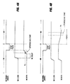
- FIG. 4A shows the end of one IM format message (indicated by the "stop” or “end of transmission” (EOT) pulse), and the beginning of another IM message.
- EOT end of transmission
- IM signals CLOCK and DATA bus lines SERBUS1 and SERBUS2, respectively, in Figure 1A
- signal DATA begins to change to logic 1 after signal CLOCK has already changed to logic 1.
- the time delay between the transitions of signals CLOCK and DATA that is shown in Figure 4A may be caused by unequal parasitic loading of the serial bus lines as described above. After passing logic switching threshold VT, signal DATA is effectively at logic 1.
- transient signals e.g. noise
- signal DATA may cause a negative-going spike in signal DATA that occurs before signal DATA completes its transition to logic 1 but after signal DATA has passed threshold VT.
- signal DATA would appear to exhibit a pulse to logic 0 while signal CLOCK is at logic 1. If the pulse is of sufficient duration and the system is connected as shown in Figure 1A, a spurious IIC start condition is created.
- Figure 4B illustrates another potential cause of bus conflicts that might occur during a sequence of IM format messages in a system connected as in Figure 1A.
- the system shown in Figure 1 might be designed such that any "forced" state on signals CLOCK and DATA at the end of an IM transmission, e.g forced to logic 1, is "released” into a tristate (high impedance) condition at the end of the IM transmission to prevent the forced state from interfering with subsequent bus transmissions.
- the tristate condition permits leakage currents to cause a relatively slow change in the value of signal DATA as shown in Figure 4B.
- the change in the value of signal DATA may be cross switching threshold VT effectively changing the state of signal DATA to logic 0. If signal CLOCK (bus line SERBUS1) is at logic 1 when the change of state occurs, a spurious IIC start condition exists in a system that is connected as in Figure 1A.
Landscapes
- Engineering & Computer Science (AREA)
- Theoretical Computer Science (AREA)
- Physics & Mathematics (AREA)
- General Engineering & Computer Science (AREA)
- General Physics & Mathematics (AREA)
- Small-Scale Networks (AREA)
- Information Transfer Systems (AREA)
- Communication Control (AREA)
Claims (3)
- Anordnung, enthaltend:einen Datenbus mit einer ersten Busleitung (SERBUS1) und einer zweiten Busleitung (SERBUS2);erste (160) und zweite (150) mit dem Datenbus verbundene Mittel zur Verarbeitung der Daten in Abhängigkeit von Signalen auf dem Datenbus; undmit dem Datenbus verbundene Steuermittel (CONTROL mC,110) zur Lieferung von Signalen zur Steuerung der Datenverarbeitung durch die ersten und die zweiten Mittel, dadurch gekennzeichnet, daß die ersten Mittel einen Takteingang (CLOCK) und einen Dateneingang (DATA) aufweisen, die mit der ersten bzw. der zweiten Busleitung verbunden sind, für die Datenverarbeitung in Abhängigkeit von an dem Takteingang und dem Dateneingang empfangenen Takt- und Datensignalen;daß die zweiten Mittel einen Takteingang (SCL) und einen Dateneingang (SDA) aufweisen, die mit der zweiten Busleitung bzw. der ersten Busleitung verbunden sind, für eine Datenverarbeitung in Abhängigkeit von an dem Takteingang und dem Dateneingang empfangenen Takt- und Datensignalen; unddaß die Steuermittel während eines ersten Operationsmodus ein Taktsignal (IM CLOCK) auf der ersten Busleitung und ein Datensignal (IM DATA) auf der zweiten Busleitung zur Steuerung der Operation der ersten Datenverarbeitungsmittel ohne Beeinflussung der Operation der zweiten Datenverarbeitungsmittel erzeugen und während eines zweiten Operationsmodus ein Datensignal (IIC DATA) auf der ersten Busleitung und ein Taktsignal (IIC CLOCK) auf der zweiten Busleitung für die Steuerung der Operation der zweiten Datenverarbeitungsmittel ohne Beeinflussung der Operation der ersten Datenverarbeitungsmittel erzeugen.
- Anordnung nach Anspruch 1, dadurch gekennzeichnet, daß die Steuermittel (CONTROL mC,110) folgendes enthalten:einen Mikroprozessor (CONTROL mC) zur Erzeugung des Datensignals während des ersten Operationsmodus und zur Erzeugung eines Steuersignals zur Anzeige, ob die Anordnung in dem ersten oder dem zweiten Operationsmodus arbeitet;ein Schieberegister (112), das während des zweiten Operationsmodus das Datensignal erzeugt; undeinen auf das Steuersignal ansprechenden Multiplexer (120, 130) zur Zuführung des Datensignals von dem Mikroprozessor zu der zweiten Busleitung während des ersten Operationsmodus und zur Zuführung des Datensignals von dem Schieberegister zu der ersten Busleitung während des zweiten Operationsmodus.
- Anordnung nach Anspruch 2, dadurch gekennzeichnet, daß der Datenbus ein serieller Datenbus ist.
Applications Claiming Priority (2)
| Application Number | Priority Date | Filing Date | Title |
|---|---|---|---|
| US947669 | 1992-09-18 | ||
| US07/947,669 US5376928A (en) | 1992-09-18 | 1992-09-18 | Exchanging data and clock lines on multiple format data buses |
Publications (2)
| Publication Number | Publication Date |
|---|---|
| EP0588191A1 EP0588191A1 (de) | 1994-03-23 |
| EP0588191B1 true EP0588191B1 (de) | 1998-03-04 |
Family
ID=25486539
Family Applications (1)
| Application Number | Title | Priority Date | Filing Date |
|---|---|---|---|
| EP93114208A Expired - Lifetime EP0588191B1 (de) | 1992-09-18 | 1993-09-04 | Austausch von Daten- und Taktleitungen auf mehrformatigen Datenbussen |
Country Status (9)
| Country | Link |
|---|---|
| US (1) | US5376928A (de) |
| EP (1) | EP0588191B1 (de) |
| JP (1) | JP2805579B2 (de) |
| KR (1) | KR100281955B1 (de) |
| CN (1) | CN1038452C (de) |
| ES (1) | ES2113458T3 (de) |
| MX (1) | MX9305711A (de) |
| MY (1) | MY109682A (de) |
| SG (1) | SG75764A1 (de) |
Families Citing this family (46)
| Publication number | Priority date | Publication date | Assignee | Title |
|---|---|---|---|---|
| JPH0738586A (ja) * | 1993-07-21 | 1995-02-07 | Brother Ind Ltd | データ伝送装置 |
| US5594874A (en) * | 1993-09-30 | 1997-01-14 | Cirrus Logic, Inc. | Automatic bus setting, sensing and switching interface unit |
| US5727184A (en) * | 1994-06-27 | 1998-03-10 | Cirrus Logic, Inc. | Method and apparatus for interfacing between peripherals of multiple formats and a single system bus |
| US5794014A (en) * | 1994-06-27 | 1998-08-11 | Cirrus Logic, Inc. | Method and apparatus for interfacing between peripherals of multiple formats and a single system bus |
| DE69515147T2 (de) | 1994-07-15 | 2000-09-21 | Thomson Consumer Electronics, Inc. | Mehrfachprotokoll-Datenbussystem |
| GB9414331D0 (en) * | 1994-07-15 | 1994-09-07 | Thomson Consumer Electronics | Combined I*C and IM bus architecture |
| US5608877A (en) * | 1995-03-24 | 1997-03-04 | Cirrus Logic, Inc. | Reset based computer bus identification method and circuit resilient to power transience |
| FR2740238B1 (fr) * | 1995-10-19 | 1997-12-05 | Sgs Thomson Microelectronics | Cellule integrable ddc dediee a un microprocesseur |
| DE19609883C1 (de) * | 1996-03-13 | 1997-10-09 | Siemens Ag | Verfahren und Anordnung zum Übertragen von systemspezifischen Daten in einem synchronen Mikroprozessorsystem |
| JPH10198633A (ja) * | 1997-01-08 | 1998-07-31 | Mitsubishi Electric Corp | シリアルデータ転送装置 |
| US6526518B1 (en) * | 1997-05-22 | 2003-02-25 | Creative Technology, Ltd. | Programmable bus |
| KR100224965B1 (ko) | 1997-07-10 | 1999-10-15 | 윤종용 | 다층 구조의 아이2씨 버스를 이용한 진단/제어 시스템 |
| FI981894A7 (fi) * | 1998-09-04 | 2000-03-05 | Nokia Multimedia Terminals Oy | Väylärakenne |
| US6622188B1 (en) * | 1998-09-30 | 2003-09-16 | International Business Machines Corporation | 12C bus expansion apparatus and method therefor |
| KR100587261B1 (ko) * | 1998-11-13 | 2006-07-25 | 엘지전자 주식회사 | 데이터 제어장치 |
| US6253268B1 (en) * | 1999-01-15 | 2001-06-26 | Telefonaktiebolaget L M Ericsson (Publ) | Method and system for multiplexing a second interface on an I2C interface |
| DE19917576A1 (de) * | 1999-04-19 | 2000-10-26 | Moeller Gmbh | Datenübertragungseinrichtung |
| US6591322B1 (en) * | 2000-08-01 | 2003-07-08 | Sun Microsystems, Inc. | Method and apparatus for connecting single master devices to a multimaster wired-and bus environment |
| CA2388067A1 (en) * | 2000-09-07 | 2002-03-14 | John Zink Company, L.L.C. | High capacity/low nox radiant wall burner |
| US20020112070A1 (en) * | 2000-12-08 | 2002-08-15 | The Boeing Company | Network controller for digitally controlling remote devices via a common bus |
| US20040225814A1 (en) * | 2001-05-29 | 2004-11-11 | Ervin Joseph J. | Method and apparatus for constructing wired-AND bus systems |
| JP4733877B2 (ja) * | 2001-08-15 | 2011-07-27 | 富士通セミコンダクター株式会社 | 半導体装置 |
| JP3844120B2 (ja) * | 2001-10-19 | 2006-11-08 | 株式会社ルネサステクノロジ | 半導体装置 |
| US6845461B1 (en) * | 2001-11-20 | 2005-01-18 | Silicon Image, Inc. | High-speed bus with embedded clock signals |
| KR20030062900A (ko) * | 2002-01-21 | 2003-07-28 | 엘지전자 주식회사 | Iic 시스템의 충돌방지방법 및 장치 |
| US20030184066A1 (en) * | 2002-03-22 | 2003-10-02 | Thomas Stierle | Synchronous communication interface sharing for communicating with a plurality of devices |
| KR100443467B1 (ko) * | 2002-05-07 | 2004-08-09 | 손권웅 | 무염 경사를 사용하여 체크무늬를 갖는 직물의 제조방법및 그 체크 무늬 직물 |
| CN101057229B (zh) * | 2004-11-16 | 2010-11-03 | Nxp股份有限公司 | 总线通信系统 |
| KR100654796B1 (ko) * | 2004-11-16 | 2006-12-08 | 삼성전자주식회사 | 데이터수신장치 및 그 제어방법 |
| US7467204B2 (en) * | 2005-02-10 | 2008-12-16 | International Business Machines Corporation | Method for providing low-level hardware access to in-band and out-of-band firmware |
| US20090020450A1 (en) * | 2007-07-16 | 2009-01-22 | Heneghan Grace A | Automotive tray |
| US7966438B2 (en) * | 2007-09-27 | 2011-06-21 | Honeywell International Inc. | Two-wire communications bus system |
| TWI474179B (zh) * | 2010-04-28 | 2015-02-21 | Hon Hai Prec Ind Co Ltd | 多設備連接系統 |
| US8667204B2 (en) * | 2011-01-24 | 2014-03-04 | Rpx Corporation | Method to differentiate identical devices on a two-wire interface |
| US8832343B2 (en) | 2012-07-17 | 2014-09-09 | International Business Machines Corporation | Double density I2C system |
| US9996488B2 (en) | 2013-09-09 | 2018-06-12 | Qualcomm Incorporated | I3C high data rate (HDR) always-on image sensor 8-bit operation indicator and buffer over threshold indicator |
| US10353837B2 (en) | 2013-09-09 | 2019-07-16 | Qualcomm Incorporated | Method and apparatus to enable multiple masters to operate in a single master bus architecture |
| US9519603B2 (en) | 2013-09-09 | 2016-12-13 | Qualcomm Incorporated | Method and apparatus to enable multiple masters to operate in a single master bus architecture |
| US9690725B2 (en) | 2014-01-14 | 2017-06-27 | Qualcomm Incorporated | Camera control interface extension with in-band interrupt |
| JP2016538624A (ja) * | 2013-10-08 | 2016-12-08 | クアルコム,インコーポレイテッド | 共有制御データバス上でのi2cスレーブデバイスとカメラ制御インターフェース拡張デバイスの共存 |
| WO2015054548A1 (en) | 2013-10-09 | 2015-04-16 | Qualcomm Incorporated | ERROR DETECTION CAPABILITY OVER CCIe PROTOCOL |
| US9684624B2 (en) | 2014-01-14 | 2017-06-20 | Qualcomm Incorporated | Receive clock calibration for a serial bus |
| CN103955419A (zh) * | 2014-04-28 | 2014-07-30 | 电子科技大学 | 具有串行总线协议在线实时检测分析功能的逻辑分析仪 |
| CN104503330A (zh) * | 2014-12-19 | 2015-04-08 | 上海发电设备成套设计研究院 | 一种基于arm的发电机励磁系统数据采集仪 |
| KR101998702B1 (ko) * | 2017-09-07 | 2019-07-10 | 주식회사 동운아나텍 | 투-와이어 버스용 슬레이브 디바이스 |
| DE112020002619T5 (de) * | 2019-05-31 | 2022-03-17 | Ams International Ag | Ein inter-integrated circuit (i2c) gerät |
Family Cites Families (7)
| Publication number | Priority date | Publication date | Assignee | Title |
|---|---|---|---|---|
| JPS5997245A (ja) * | 1982-11-26 | 1984-06-05 | Fujitsu Ltd | 二重化された時分割多元接続方式の通信装置における同期方式 |
| WO1985003147A1 (en) * | 1984-01-13 | 1985-07-18 | Term-Tronics Incorporated | Generic communications terminal |
| ATE73558T1 (de) * | 1984-08-23 | 1992-03-15 | Siemens Ag | Datenuebertragungsverfahren ueber einen multiprozessorbus. |
| DE3789743T2 (de) * | 1986-09-01 | 1994-08-18 | Nippon Electric Co | Serielles Datenübertragungssystem. |
| US4855905A (en) * | 1987-04-29 | 1989-08-08 | International Business Machines Corporation | Multiprotocol I/O communications controller unit including emulated I/O controllers and tables translation of common commands and device addresses |
| US4792950A (en) * | 1987-06-17 | 1988-12-20 | Ford Motor Company | Multiplex wiring system |
| ES2047523T3 (es) * | 1988-09-22 | 1994-03-01 | Siemens Ag | Procedimiento para el funcionamiento de instalaciones de conmutacion de telecomunicaciones temporal controladas por impulsos de reloj, especialmente instalaciones de conmutacion telefonica-pcm, con campo de acoplamiento central y campos de acoplamiento parcial conectados. |
-
1992
- 1992-09-18 US US07/947,669 patent/US5376928A/en not_active Expired - Lifetime
-
1993
- 1993-08-05 MY MYPI93001543A patent/MY109682A/en unknown
- 1993-09-04 SG SG1996002450A patent/SG75764A1/en unknown
- 1993-09-04 EP EP93114208A patent/EP0588191B1/de not_active Expired - Lifetime
- 1993-09-04 ES ES93114208T patent/ES2113458T3/es not_active Expired - Lifetime
- 1993-09-15 KR KR1019930018507A patent/KR100281955B1/ko not_active Expired - Fee Related
- 1993-09-17 JP JP5263991A patent/JP2805579B2/ja not_active Expired - Fee Related
- 1993-09-17 MX MX9305711A patent/MX9305711A/es not_active IP Right Cessation
- 1993-09-18 CN CN93118005A patent/CN1038452C/zh not_active Expired - Fee Related
Also Published As
| Publication number | Publication date |
|---|---|
| KR100281955B1 (ko) | 2001-02-15 |
| JP2805579B2 (ja) | 1998-09-30 |
| US5376928A (en) | 1994-12-27 |
| EP0588191A1 (de) | 1994-03-23 |
| SG75764A1 (en) | 2000-10-24 |
| MY109682A (en) | 1997-04-30 |
| MX9305711A (es) | 1994-05-31 |
| CN1038452C (zh) | 1998-05-20 |
| ES2113458T3 (es) | 1998-05-01 |
| KR940007698A (ko) | 1994-04-27 |
| JPH06205072A (ja) | 1994-07-22 |
| CN1084986A (zh) | 1994-04-06 |
Similar Documents
| Publication | Publication Date | Title |
|---|---|---|
| US5376928A (en) | Exchanging data and clock lines on multiple format data buses | |
| EP0693729B1 (de) | Mehrfachprotokoll-Datenbussystem | |
| US5852406A (en) | Multi-protocol data bus system | |
| US6339806B1 (en) | Primary bus to secondary bus multiplexing for I2C and other serial buses | |
| US6687769B2 (en) | Serial peripheral interface with high performance buffering scheme | |
| CN1132381C (zh) | 用于在集成电路和其它设备之间传递数据的方法和系统 | |
| US4106091A (en) | Interrupt status indication logic for polled interrupt digital system | |
| EP0740253B1 (de) | Kommunikationsschnittstelle mittels einer Softwaresimulation eines UARTs | |
| WO1998011693A2 (en) | Low power serial protocol translator for use in multi-circuit board electronic systems | |
| US6557062B1 (en) | System and method for low-noise control of radio frequency devices | |
| KR100417186B1 (ko) | 업그레이드 장치 설치 시 그래픽 버스 상의 부하 균형유지 방법 및 장치 | |
| US5577201A (en) | Diagnostic protocol and display system | |
| US5608883A (en) | Adapter for interconnecting single-ended and differential SCSI buses to prevent `busy` or `wired-or` glitches from being passed from one bus to the other | |
| WO2005106689A1 (en) | Bus system for selectively controlling a plurality of identical slave circuits connected to the bus and method therefore | |
| US4006457A (en) | Logic circuitry for selection of dedicated registers | |
| US6438624B1 (en) | Configurable I/O expander addressing for I/O drawers in a multi-drawer rack server system | |
| JPH0884154A (ja) | バスラインシステム | |
| US7009380B2 (en) | Interface device for product testing | |
| US6003096A (en) | Host interface circuit for preventing data loss and improving interface speed for an image forming apparatus by latching received data in response to a strobe input signal | |
| JPH10207834A (ja) | シリアル入出力回路 | |
| US5249287A (en) | General keyboard interface for operating with two types of keyboards | |
| US7020726B2 (en) | Methods and apparatus for signaling to switch between different bus bandwidths | |
| KR101023280B1 (ko) | 데이터 통신 시스템 | |
| KR0181596B1 (ko) | I2c 버스의 데이터 전송 장치 및 방법 | |
| JPH117414A (ja) | 半導体集積回路 |
Legal Events
| Date | Code | Title | Description |
|---|---|---|---|
| PUAI | Public reference made under article 153(3) epc to a published international application that has entered the european phase |
Free format text: ORIGINAL CODE: 0009012 |
|
| AK | Designated contracting states |
Kind code of ref document: A1 Designated state(s): ES GB IT PT |
|
| 17P | Request for examination filed |
Effective date: 19940827 |
|
| GRAG | Despatch of communication of intention to grant |
Free format text: ORIGINAL CODE: EPIDOS AGRA |
|
| 17Q | First examination report despatched |
Effective date: 19970306 |
|
| GRAG | Despatch of communication of intention to grant |
Free format text: ORIGINAL CODE: EPIDOS AGRA |
|
| GRAH | Despatch of communication of intention to grant a patent |
Free format text: ORIGINAL CODE: EPIDOS IGRA |
|
| GRAH | Despatch of communication of intention to grant a patent |
Free format text: ORIGINAL CODE: EPIDOS IGRA |
|
| GRAA | (expected) grant |
Free format text: ORIGINAL CODE: 0009210 |
|
| AK | Designated contracting states |
Kind code of ref document: B1 Designated state(s): ES GB IT PT |
|
| ITF | It: translation for a ep patent filed | ||
| REG | Reference to a national code |
Ref country code: ES Ref legal event code: FG2A Ref document number: 2113458 Country of ref document: ES Kind code of ref document: T3 |
|
| REG | Reference to a national code |
Ref country code: PT Ref legal event code: SC4A Free format text: AVAILABILITY OF NATIONAL TRANSLATION Effective date: 19980529 |
|
| PLBE | No opposition filed within time limit |
Free format text: ORIGINAL CODE: 0009261 |
|
| 26N | No opposition filed | ||
| REG | Reference to a national code |
Ref country code: GB Ref legal event code: IF02 |
|
| REG | Reference to a national code |
Ref country code: GB Ref legal event code: 746 Effective date: 20030103 |
|
| PGFP | Annual fee paid to national office [announced via postgrant information from national office to epo] |
Ref country code: IT Payment date: 20070926 Year of fee payment: 15 Ref country code: ES Payment date: 20071024 Year of fee payment: 15 |
|
| REG | Reference to a national code |
Ref country code: PT Ref legal event code: MM4A Free format text: LAPSE DUE TO NON-PAYMENT OF FEES Effective date: 20090304 |
|
| PG25 | Lapsed in a contracting state [announced via postgrant information from national office to epo] |
Ref country code: PT Free format text: LAPSE BECAUSE OF NON-PAYMENT OF DUE FEES Effective date: 20090304 |
|
| PG25 | Lapsed in a contracting state [announced via postgrant information from national office to epo] |
Ref country code: IT Free format text: LAPSE BECAUSE OF NON-PAYMENT OF DUE FEES Effective date: 20080904 |
|
| REG | Reference to a national code |
Ref country code: ES Ref legal event code: FD2A Effective date: 20080905 |
|
| PGFP | Annual fee paid to national office [announced via postgrant information from national office to epo] |
Ref country code: PT Payment date: 20070904 Year of fee payment: 15 Ref country code: GB Payment date: 20090827 Year of fee payment: 17 |
|
| PG25 | Lapsed in a contracting state [announced via postgrant information from national office to epo] |
Ref country code: ES Free format text: LAPSE BECAUSE OF NON-PAYMENT OF DUE FEES Effective date: 20080905 |
|
| GBPC | Gb: european patent ceased through non-payment of renewal fee |
Effective date: 20100904 |
|
| PG25 | Lapsed in a contracting state [announced via postgrant information from national office to epo] |
Ref country code: GB Free format text: LAPSE BECAUSE OF NON-PAYMENT OF DUE FEES Effective date: 20100904 |