EP0565869B1 - Matrixförmige Anzeigevorrichtung - Google Patents
Matrixförmige Anzeigevorrichtung Download PDFInfo
- Publication number
- EP0565869B1 EP0565869B1 EP93103968A EP93103968A EP0565869B1 EP 0565869 B1 EP0565869 B1 EP 0565869B1 EP 93103968 A EP93103968 A EP 93103968A EP 93103968 A EP93103968 A EP 93103968A EP 0565869 B1 EP0565869 B1 EP 0565869B1
- Authority
- EP
- European Patent Office
- Prior art keywords
- column
- setting
- lines
- resetting
- matrix
- Prior art date
- Legal status (The legal status is an assumption and is not a legal conclusion. Google has not performed a legal analysis and makes no representation as to the accuracy of the status listed.)
- Expired - Lifetime
Links
Images

Classifications
-
- G—PHYSICS
- G09—EDUCATION; CRYPTOGRAPHY; DISPLAY; ADVERTISING; SEALS
- G09G—ARRANGEMENTS OR CIRCUITS FOR CONTROL OF INDICATING DEVICES USING STATIC MEANS TO PRESENT VARIABLE INFORMATION
- G09G3/00—Control arrangements or circuits, of interest only in connection with visual indicators other than cathode-ray tubes
- G09G3/20—Control arrangements or circuits, of interest only in connection with visual indicators other than cathode-ray tubes for presentation of an assembly of a number of characters, e.g. a page, by composing the assembly by combination of individual elements arranged in a matrix no fixed position being assigned to or needed to be assigned to the individual characters or partial characters
- G09G3/34—Control arrangements or circuits, of interest only in connection with visual indicators other than cathode-ray tubes for presentation of an assembly of a number of characters, e.g. a page, by composing the assembly by combination of individual elements arranged in a matrix no fixed position being assigned to or needed to be assigned to the individual characters or partial characters by control of light from an independent source
- G09G3/3486—Control arrangements or circuits, of interest only in connection with visual indicators other than cathode-ray tubes for presentation of an assembly of a number of characters, e.g. a page, by composing the assembly by combination of individual elements arranged in a matrix no fixed position being assigned to or needed to be assigned to the individual characters or partial characters by control of light from an independent source using light modulating elements actuated by a magnetic field
-
- G—PHYSICS
- G09—EDUCATION; CRYPTOGRAPHY; DISPLAY; ADVERTISING; SEALS
- G09F—DISPLAYING; ADVERTISING; SIGNS; LABELS OR NAME-PLATES; SEALS
- G09F9/00—Indicating arrangements for variable information in which the information is built-up on a support by selection or combination of individual elements
- G09F9/30—Indicating arrangements for variable information in which the information is built-up on a support by selection or combination of individual elements in which the desired character or characters are formed by combining individual elements
- G09F9/305—Indicating arrangements for variable information in which the information is built-up on a support by selection or combination of individual elements in which the desired character or characters are formed by combining individual elements being the ends of optical fibres
Definitions
- the invention relates to a display device according to the preamble of claim 1.
- a display device of this type is known from DE 89 13 499 U1.
- nested individual matrices are assigned their own partial control devices, to which partial display information is supplied by a central control.
- the display information is composed of the partial display information.
- the sub-control devices control the assigned sub-pixels via their own control lines.
- This type of control of a matrix with four nested sub-matrices not only requires a high level of control effort, but also complex wiring of the matrix.
- the setting of the matrix is only quick if the partial control devices control all partial pixels to be set in parallel. However, this entails a high outlay on set switches in the partial control devices, since a separate set switch must be provided for each partial pixel.
- DE 40 24 499 C1 describes a circuit arrangement for a display device with a matrix of bistable matrix points is known in which the columns or the rows are controlled one after the other for checking, wherein all matrix points of the column or each row are always set or reset. With this circuit arrangement, however, no display can be set and deleted since, as a rule, only a part of the matrix points of a column or row is set in a display. In addition, a matrix point can only be displayed in one color.
- the electromagnets of the flaps can be controlled one after the other in the column direction by means of a column control device, the reset reference potential in each case in a first sub-step and the set reference potential in a second sub-step, and that in In the row direction, the electromagnets of the flaps can be controlled in parallel by means of a row control device, the reset potential being able to be switched to all half rows in the first partial step of a column control and the partial display information corresponding to the controlled half column being set to the respective assigned half rows in the second partial step of the column control, or in the same advantageous manner in that the electromagnets of the flaps can be controlled one after the other in the column direction by means of a column control device, wherein the reset reference potential in each case in a reset cycle to the controlled half column and with each column control, the reset potential can be switched on simultaneously on all half rows by means of a row control device, and that in a setting cycle, the electromagnets of the flaps can be controlled one after
- all partial matrices can be set in a control cycle with the corresponding half-column partial display information.
- the control lines in the column direction are based on the number of half columns, i.e. twice the number of columns in the matrix, and the control lines in the row direction are reduced to the number of the matrix.
- the control works in series and in the row direction in parallel, so that both the setting and the resetting of the partial pixels can be carried out very quickly, especially since the set and reset pulses only have to be applied for a few milliseconds to actuate the flaps.
- the structure of the matrix is designed in such a way that each half line has both a reset line and a set line, and that each reset line is connected to the one connections of all the electromagnets of the flaps of the assigned half line via rectifiers that are permeable to the reset potential, so that each set line via rectifier which is permeable to the setting potential is connected to the one connections of all the electromagnets of the flaps of the assigned half-line, that the other connections of the electromagnets of the flaps are assigned to Half-column lines are switched on, and that the column control device has half-column-specific reset switches and half-column-specific set switches and the row control device have half-line individual reset switches and half-line individual set switches.
- the column controller and the row controller are from a display controller, e.g. a processor, which can be supplied with the display information from a memory in the form of half-column-specific partial display information.
- a display controller e.g. a processor
- the memory contains the display information in half columns and half lines as values "0" and "1", the value "1" meaning that the assigned flap is set in the release position.
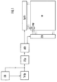
- a column control device SpSt and a row control device ZSt are assigned to a matrix M with matrix points mp consisting of four differently colored partial picture elements.
- a central display control device ASt controls the column control device SpSt and the row control device ZSt.
- An input EG specifies which display information is to be displayed with the matrix M.
- Various display information is stored in a memory ZSp.
- a specific text can also be selected using a TxSp text memory.
- the memory ZSp then converts the letters of the text into partial display information and places them in the fields specified in the matrix M.
- Each sub-pixel of the matrix point mp has an optical fiber which is illuminated in accordance with the color assigned to the sub-matrix.
- the optical fibers of a sub-matrix can be combined to form an optical fiber bundle and at the same time illuminated by an appropriate filter.
- the light exit end of each optical fiber can be covered and released by means of a flap, so that the image partial point with the assigned color can be included in the display or eliminated from the display.
- the partial image point b1 white, the partial pixel b2 is yellow, the partial pixel b3 is green and the partial pixel is red.
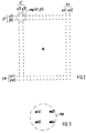
- This arrangement of a matrix point mp is repeated over all columns x1 to xn and over all rows y1 to ym.
- the columns x1 to xn are divided into half columns x11, x12 to xn1, xn2 with assigned control lines and the lines y1 to ym into half lines y11, y12 to ym1, ym2 with assigned control lines.
- the control information present or supplied in the display control device ASt corresponds to the display information, the value "0" meaning a covered optical fiber and the value "1" indicating an enabled optical fiber.
- the structure of the control information corresponds to the structure of the matrix M with the columns x1 to xn and the half columns x11, x12 to xn1, xn2 and with the lines y1 to ym and the half lines y11, y12 to ym1, ym2.
- a half column x11, x12 to xn1, xn2 forms part display information TInf, which is transmitted in parallel into the assigned half column x11, x12 to xn1, xn2 of the matrix M.
- the display information can be divided into fields B1, B2, B3, B4 ... of the same size.
- the fields B1, B2, B3, B4 ... are so large that a letter of a text can be displayed. If a certain text is specified with the text memory TxSp, then the memory ZSp can be used to convert the corresponding partial display information letter by letter.
- the display control device ASt positions the partial display information in the assigned field B1, B2, B3, B4 ... of the matrix M. This process is repeated until the text letter by letter in the matrix M in the corresponding fields B1, B2, B3, B4 ... is set.
- FIG. 5 shows the electrical structure of a matrix point mp (x1, y1) with the four electromagnets Kx11y11, Kx12y11, Kx11y12 and Kx12y12 of the flaps. These electromagnets of the flaps are connected to one of the connections on the assigned control lines of the half columns x11 and x12. The respective other connections lead via two rectifiers Ds and Dr to the set line and the reset line of the assigned half line y11 or y12.
- the Kx11y11 electromagnet of the flap is assigned to the half column x11 and the half line y11, the electromagnet Kx12y11 of the flap of the half column x12 and the half line y11, the electromagnet Kx11y12 of the half column x11 and the half line y12 and the electromagnet Kx12y12 of the flap of the half column x12 and the half line y12.
- the half line y11 has a set line y11s and a reset line y11r and the half line y12 has a set line y12s and a reset line y12r.
- Each set line y11s or y12s is assigned a set switch shz1 or shz2, which connects the set potential + to the set line y11s or y12s via the rectifier Ds.
- the selected half column x11 or x12 is switched to the setting reference potential ground via setting switch shsp1 or shsp2.
- Each reset line y11r or y12r is assigned a reset switch rhz1 or rhz2, which connects the reset reference potential ground to the reset line rhz1 or rhz2 via the rectifier Dr.
- the selected half column x11 or x12 is switched on to the reset potential + via a reset switch rhsp1 or rhsp2.
- the rectifiers Ds and Dr are switched on in such a way that when the current is set or reset the current flows in one direction or the other via the electromagnet of the flap. A brief impulse is sufficient. The flap is then held in the set position by remanence until the solenoid is actuated in the other current direction.
- the control cycle can be done in two ways. This means that setting and resetting can include a separate cycle. Before setting new display information, all flaps are reset to the cover position. This is done in that the half-columns x11, x12 to xn1, xn2 are successively applied with the reset potential + via their reset switches rhsp1 or rhsp2. Each time a half column x11, x12 to xn1, xn2 is activated, all reset lines y11r or y12r are always supplied with reset reference potential ground via the reset switches rhz1 or rhz2. All flaps of the selected half column are reset to their cover positions in one step.
- the flaps can be set from half column to half column in accordance with the display information according to FIG. 4 in a setting cycle.
- the information assigned to the matrix point mp (x1, y1) will lead to the setting of the electromagnet Kx11y12 of the assigned flap when the half-column x11 is activated and to the setting of the electromagnet Kx12y11 of the assigned flap when the half-column x12 is activated.
- all partial display information TInf of the display information is transferred into the half columns x11, x12 to xn1, xn2 of the matrix M.
- the assigned flaps release the partial pixels and the matrix M shows the corresponding display.
- the partial pixels of each matrix point mp can be set as desired or not set.
- the set cycle and the reset cycle can also be nested.
- the half column x11, x12 to xn1, xn2 is first reset in a first partial step and then set in accordance with the assigned partial display information TInf.
- This has the advantage that the half column x11, x12 to xn1, xn2 only has to be addressed once.
- the resetting and setting process is repeated until the cycle on the last half column x11, x12 to xn1, xn2 is completed and ended. New display information is then overwritten from half column to half column.
Applications Claiming Priority (2)
| Application Number | Priority Date | Filing Date | Title |
|---|---|---|---|
| DE4212125A DE4212125C1 (xx) | 1992-04-13 | 1992-04-13 | |
| DE4212125 | 1992-04-13 |
Publications (3)
| Publication Number | Publication Date |
|---|---|
| EP0565869A2 EP0565869A2 (de) | 1993-10-20 |
| EP0565869A3 EP0565869A3 (xx) | 1994-04-06 |
| EP0565869B1 true EP0565869B1 (de) | 1996-07-31 |
Family
ID=6456580
Family Applications (1)
| Application Number | Title | Priority Date | Filing Date |
|---|---|---|---|
| EP93103968A Expired - Lifetime EP0565869B1 (de) | 1992-04-13 | 1993-03-11 | Matrixförmige Anzeigevorrichtung |
Country Status (7)
| Country | Link |
|---|---|
| US (1) | US5406302A (xx) |
| EP (1) | EP0565869B1 (xx) |
| AT (1) | ATE141021T1 (xx) |
| CA (1) | CA2093897C (xx) |
| DE (2) | DE4212125C1 (xx) |
| NO (1) | NO931348L (xx) |
| SG (1) | SG46533A1 (xx) |
Families Citing this family (2)
| Publication number | Priority date | Publication date | Assignee | Title |
|---|---|---|---|---|
| US5793349A (en) * | 1992-03-20 | 1998-08-11 | Mark Iv Industries Limited | Electromagnetic shutter and cover |
| WO1998054689A1 (fr) * | 1997-05-29 | 1998-12-03 | Shozo Hirayama | Dispositif optique d'affichage d'images par points |
Family Cites Families (41)
| Publication number | Priority date | Publication date | Assignee | Title |
|---|---|---|---|---|
| AT36086B (de) | 1907-09-07 | 1909-02-10 | Metall Ind Winter & Adler Ag | Einrichtung zur Lagerung der Verschlußklappe für die Ausgabeöffnung von Dosen. |
| US2589569A (en) * | 1948-08-04 | 1952-03-18 | Westinghouse Brake & Signal | Optical system for use in light signals, indicators, and the like |
| US3389389A (en) * | 1965-01-11 | 1968-06-18 | Neonix Inc | Moving message sign |
| US3553645A (en) * | 1968-04-04 | 1971-01-05 | William P Finkel | Variable message traffic sign |
| JPS4941692B1 (xx) * | 1968-11-27 | 1974-11-11 | ||
| DE2226959C3 (de) * | 1972-06-02 | 1980-10-02 | Siemens Ag, 1000 Berlin Und 8000 Muenchen | Farbige Datenanzeige |
| GB1464001A (en) * | 1973-03-07 | 1977-02-09 | Buchert C | Data display panels |
| US3962702A (en) * | 1974-03-01 | 1976-06-08 | Jenaer Glaswerk Schott & Gen. | Optical fiber display device |
| GB1473068A (en) * | 1975-04-30 | 1977-05-11 | Rank Organisation Ltd | Face plate graticule |
| US4163332B2 (en) * | 1976-10-05 | 1995-09-05 | Unisplay Sa | Matrix display device |
| US4106231A (en) * | 1976-12-06 | 1978-08-15 | Master Specialties Company | Low level light indicator |
| DE2831174A1 (de) * | 1977-07-15 | 1979-01-18 | Kawaguchiko Seimitsu Kk | Leuchtanzeige-vorrichtung |
| GB2051447A (en) * | 1979-06-14 | 1981-01-14 | Rank Organisation Ltd | Optical display apparatus |
| US4299447A (en) * | 1979-06-27 | 1981-11-10 | The United States Of America As Represented By The Secretary Of The Navy | Liquid crystal fiber optics large screen display panel |
| DE7931474U1 (de) * | 1979-11-07 | 1980-04-03 | Landsrath, Walter, 6600 Saarbruecken | Windanzeigeeinrichtung fuer strassenbruecken u.dgl. |
| DE3012816C2 (de) * | 1980-04-02 | 1984-12-13 | Friedrich Merk-Telefonbau GmbH, 8000 München | Alphanumerisches Anzeigesystem für Fahrzeuge |
| DE3021502A1 (de) * | 1980-06-07 | 1981-12-24 | Friedrich Merk Telefonbau GmbH, 8000 München | Bistabile elektromagnetische schauzeichen |
| DE3031246A1 (de) * | 1980-08-19 | 1982-03-25 | Bruno 6721 Harthausen Frittel | Warn- oder hinweiseinrichtung, insbesondere fuer den strassenverkehr |
| DE3128329A1 (de) * | 1981-07-17 | 1983-01-27 | Ruhrkohle Ag, 4300 Essen | Wechselzeichen-signalgabevorrichtung fuer explosionsgefaehrdete bereiche, insbesondere grubenbaue |
| DE8124380U1 (de) * | 1981-08-20 | 1983-03-24 | Siemens AG, 1000 Berlin und 8000 München | Wechselanzeigeeinrichtung, insbesondere fuer verkehrssignalanzeigen |
| DE3303917A1 (de) * | 1983-02-05 | 1984-08-09 | Robert Bosch Gmbh, 7000 Stuttgart | Anzeigevorrichtung |
| JPS59147389A (ja) * | 1983-02-10 | 1984-08-23 | シャープ株式会社 | ドツトマトリツクス表示装置 |
| DE3319179A1 (de) * | 1983-05-21 | 1985-01-24 | Joachim Dipl.-Phys. 5020 Frechen Schick | Lichtleitersystem fuer z.b. kraftfahrzeugrueckleuchtgruppen |
| DE8318633U1 (de) * | 1983-06-28 | 1983-12-08 | Pintsch Bamag Antriebs- Und Verkehrstechnik Gmbh, 4220 Dinslaken | Faseroptischer zeichengeber |
| US4794391A (en) * | 1983-10-31 | 1988-12-27 | Securite Et Signalisation | Display matrix incorporating light-conducting fibers and light-occulting shutters |
| ATE36086T1 (de) * | 1983-11-23 | 1988-08-15 | Cetehor | Leuchtanzeigeanordnung. |
| DE3434355A1 (de) * | 1984-09-19 | 1986-06-12 | Nauschütt, Jürgen, 3000 Hannover | Leuchtanzeigetafel, gebildet aus einer vielzahl von leuchtelementen, die aus den enden von lichtleitern bestehen |
| US4747648A (en) * | 1985-01-24 | 1988-05-31 | Drd Ltd. | Optical fiber display and optical train for same |
| DE3511839A1 (de) * | 1985-03-30 | 1986-10-02 | Braun Ag, 6000 Frankfurt | Lichtleiter zum beleuchten von geraeteanzeigen |
| FR2585164B1 (fr) * | 1985-07-22 | 1988-04-22 | Soc Et Dev Prod Electron | Cellule elementaire d'affichage pour panneau d'affichage a matrice de points |
| US4839635A (en) * | 1987-01-12 | 1989-06-13 | Inwave Corporation | Signboard for displaying optical images |
| EP0324147A3 (en) * | 1988-01-11 | 1990-07-04 | Seiko Epson Corporation | Light guide type display apparatus |
| DE3812418A1 (de) * | 1988-04-14 | 1989-10-26 | Hoechst Ag | Faseroptische leuchtzeichenanlage |
| CA1298082C (en) * | 1988-06-29 | 1992-03-31 | Nei Canada Limited | Fibre optic display device |
| US4914427A (en) * | 1988-11-03 | 1990-04-03 | The Staver Company Inc. | Matrix display system and method |
| NL8900093A (nl) * | 1989-01-16 | 1990-08-16 | Nederland Haarlem B V | Lichtsignaalgever voor signaleringsdoeleinden. |
| US4965488A (en) * | 1989-03-27 | 1990-10-23 | Bachir Hihi | Light-source multiplication device |
| DE8913499U1 (xx) * | 1989-05-19 | 1990-02-08 | Dambach-Werke Gmbh, 7560 Gaggenau, De | |
| ATE107787T1 (de) * | 1989-05-19 | 1994-07-15 | Dambach Werke Gmbh | Anzeigevorrichtung für alphanumerische anzeigen. |
| US5055832A (en) * | 1989-06-09 | 1991-10-08 | Dayco Products Canada Inc. | Display element with notched disk |
| DE4024499C1 (xx) * | 1990-08-02 | 1991-09-26 | Dambach-Werke Gmbh, 7560 Gaggenau, De |
-
1992
- 1992-04-13 DE DE4212125A patent/DE4212125C1/de not_active Expired - Fee Related
-
1993
- 1993-03-11 DE DE59303346T patent/DE59303346D1/de not_active Expired - Fee Related
- 1993-03-11 AT AT93103968T patent/ATE141021T1/de not_active IP Right Cessation
- 1993-03-11 EP EP93103968A patent/EP0565869B1/de not_active Expired - Lifetime
- 1993-03-11 SG SG1996005689A patent/SG46533A1/en unknown
- 1993-04-07 NO NO93931348A patent/NO931348L/no unknown
- 1993-04-08 US US08/045,491 patent/US5406302A/en not_active Expired - Lifetime
- 1993-04-13 CA CA002093897A patent/CA2093897C/en not_active Expired - Fee Related
Also Published As
| Publication number | Publication date |
|---|---|
| DE4212125C1 (xx) | 1993-04-01 |
| US5406302A (en) | 1995-04-11 |
| NO931348L (no) | 1993-10-14 |
| NO931348D0 (no) | 1993-04-07 |
| DE59303346D1 (de) | 1996-09-05 |
| CA2093897C (en) | 1998-07-21 |
| EP0565869A2 (de) | 1993-10-20 |
| EP0565869A3 (xx) | 1994-04-06 |
| SG46533A1 (en) | 1998-02-20 |
| ATE141021T1 (de) | 1996-08-15 |
| CA2093897A1 (en) | 1993-10-14 |
Similar Documents
| Publication | Publication Date | Title |
|---|---|---|
| DE2701277C3 (de) | Wiedergabevorrichtung für graphische Symbole | |
| DE2246047C3 (de) | Elektrische farbige Darstellungsanordnung zur visuellen Darstellung eines Musters | |
| DE3514821A1 (de) | Anzeigesteuerschaltung zur steuerung von mindestens zwei unterschiedlichen anzeigeeinrichtungen | |
| DE2645535A1 (de) | Multiadressdigitalspeicher | |
| EP0584895B1 (de) | Verfahren zum signaltechnisch sicheren Anzeigen verkehrstechnischer Informationen eines Verkehrswegesystems | |
| DE3607945A1 (de) | Bedienungspult fuer drucker, insbesondere fuer matrixdrucker | |
| EP0565869B1 (de) | Matrixförmige Anzeigevorrichtung | |
| DE2944144C2 (xx) | ||
| DE3024452A1 (de) | Einrichtung zur anzeige der elektrisch erfassbaren stellungen bzw. einstellungen einzelner fuer den druckprozess benoetigten einrichtungen | |
| DE3733930C2 (xx) | ||
| DE1799009C2 (de) | Datenverarbeitungs- und Anzeigevorrichtung | |
| DE1474077B2 (de) | Anordnung zur Eingabe von Informationen in ein Datenverarbeitungsgerät durch Markieren eines Punktes auf einer Katodenstrahlröhre | |
| DE2126013A1 (de) | Vorrichtung zur Zeichendarstellung mittels Kathodenstrahlröhren | |
| DE1943770A1 (de) | Verfahren und Vorrichtung zum Entwurf von farbigen Mustern,insbesondere Textilmustern od.dgl. sowie zur Speicherung der Darstellung in Lochstreifen oder anderen Informationstraegern | |
| AT399135B (de) | Vorrichtung zur signaltechnisch sicheren darstellung eines bildes auf einem datensichtgerät | |
| DE3046513C2 (de) | Verfahren und Anordnung zum Speichern von graphischen Mustern | |
| DE3838469A1 (de) | Anzeigevorrichtung | |
| EP0308813B1 (de) | Einrichtung zur Anzeige von Zeichen | |
| DE3917077A1 (de) | Farbmosaik-anzeigetafel | |
| DE4219925C1 (xx) | ||
| DE2056844C3 (de) | Anordnung zur Darstellung von Bildern | |
| DE1774884C (de) | Zeichen-Signalgenerator | |
| DE1487857C3 (de) | Schaltungsanordnung zur Steuerung dezentraler Einrichtungen in Fernmelde-, insbesondere Fernsprechanlagen | |
| DE10346931B4 (de) | Leuchtdioden-Steuerung | |
| AT242568B (de) | Lichtschreiber-Einrichtung |
Legal Events
| Date | Code | Title | Description |
|---|---|---|---|
| PUAI | Public reference made under article 153(3) epc to a published international application that has entered the european phase |
Free format text: ORIGINAL CODE: 0009012 |
|
| AK | Designated contracting states |
Kind code of ref document: A2 Designated state(s): AT BE CH DE DK ES FR GB GR IT LI LU NL SE |
|
| PUAL | Search report despatched |
Free format text: ORIGINAL CODE: 0009013 |
|
| AK | Designated contracting states |
Kind code of ref document: A3 Designated state(s): AT BE CH DE DK ES FR GB GR IT LI LU NL SE |
|
| 17P | Request for examination filed |
Effective date: 19940305 |
|
| 17Q | First examination report despatched |
Effective date: 19951006 |
|
| GRAH | Despatch of communication of intention to grant a patent |
Free format text: ORIGINAL CODE: EPIDOS IGRA |
|
| GRAA | (expected) grant |
Free format text: ORIGINAL CODE: 0009210 |
|
| AK | Designated contracting states |
Kind code of ref document: B1 Designated state(s): AT BE CH DE DK ES FR GB GR IT LI LU NL SE |
|
| PG25 | Lapsed in a contracting state [announced via postgrant information from national office to epo] |
Ref country code: IT Free format text: LAPSE BECAUSE OF FAILURE TO SUBMIT A TRANSLATION OF THE DESCRIPTION OR TO PAY THE FEE WITHIN THE PRESCRIBED TIME-LIMIT;WARNING: LAPSES OF ITALIAN PATENTS WITH EFFECTIVE DATE BEFORE 2007 MAY HAVE OCCURRED AT ANY TIME BEFORE 2007. THE CORRECT EFFECTIVE DATE MAY BE DIFFERENT FROM THE ONE RECORDED. Effective date: 19960731 Ref country code: GR Free format text: LAPSE BECAUSE OF FAILURE TO SUBMIT A TRANSLATION OF THE DESCRIPTION OR TO PAY THE FEE WITHIN THE PRESCRIBED TIME-LIMIT Effective date: 19960731 Ref country code: FR Effective date: 19960731 Ref country code: ES Free format text: THE PATENT HAS BEEN ANNULLED BY A DECISION OF A NATIONAL AUTHORITY Effective date: 19960731 Ref country code: DK Effective date: 19960731 |
|
| REF | Corresponds to: |
Ref document number: 141021 Country of ref document: AT Date of ref document: 19960815 Kind code of ref document: T |
|
| REG | Reference to a national code |
Ref country code: CH Ref legal event code: NV Representative=s name: PATENTANWALTSBUERO FELDMANN AG |
|
| GBT | Gb: translation of ep patent filed (gb section 77(6)(a)/1977) |
Effective date: 19960809 |
|
| REF | Corresponds to: |
Ref document number: 59303346 Country of ref document: DE Date of ref document: 19960905 |
|
| PG25 | Lapsed in a contracting state [announced via postgrant information from national office to epo] |
Ref country code: SE Effective date: 19961031 |
|
| EN | Fr: translation not filed | ||
| PG25 | Lapsed in a contracting state [announced via postgrant information from national office to epo] |
Ref country code: LU Free format text: LAPSE BECAUSE OF NON-PAYMENT OF DUE FEES Effective date: 19970331 Ref country code: BE Effective date: 19970331 |
|
| PLBE | No opposition filed within time limit |
Free format text: ORIGINAL CODE: 0009261 |
|
| STAA | Information on the status of an ep patent application or granted ep patent |
Free format text: STATUS: NO OPPOSITION FILED WITHIN TIME LIMIT |
|
| 26N | No opposition filed | ||
| PGFP | Annual fee paid to national office [announced via postgrant information from national office to epo] |
Ref country code: DE Payment date: 19971004 Year of fee payment: 5 |
|
| PGFP | Annual fee paid to national office [announced via postgrant information from national office to epo] |
Ref country code: GB Payment date: 19971218 Year of fee payment: 6 |
|
| PGFP | Annual fee paid to national office [announced via postgrant information from national office to epo] |
Ref country code: AT Payment date: 19980330 Year of fee payment: 6 |
|
| PGFP | Annual fee paid to national office [announced via postgrant information from national office to epo] |
Ref country code: NL Payment date: 19980331 Year of fee payment: 6 |
|
| PGFP | Annual fee paid to national office [announced via postgrant information from national office to epo] |
Ref country code: CH Payment date: 19980701 Year of fee payment: 6 |
|
| PG25 | Lapsed in a contracting state [announced via postgrant information from national office to epo] |
Ref country code: DE Free format text: LAPSE BECAUSE OF NON-PAYMENT OF DUE FEES Effective date: 19981201 |
|
| PG25 | Lapsed in a contracting state [announced via postgrant information from national office to epo] |
Ref country code: GB Free format text: LAPSE BECAUSE OF NON-PAYMENT OF DUE FEES Effective date: 19990311 Ref country code: AT Free format text: LAPSE BECAUSE OF NON-PAYMENT OF DUE FEES Effective date: 19990311 |
|
| PG25 | Lapsed in a contracting state [announced via postgrant information from national office to epo] |
Ref country code: LI Free format text: LAPSE BECAUSE OF NON-PAYMENT OF DUE FEES Effective date: 19990331 Ref country code: CH Free format text: LAPSE BECAUSE OF NON-PAYMENT OF DUE FEES Effective date: 19990331 |
|
| PG25 | Lapsed in a contracting state [announced via postgrant information from national office to epo] |
Ref country code: NL Free format text: LAPSE BECAUSE OF NON-PAYMENT OF DUE FEES Effective date: 19991001 |
|
| GBPC | Gb: european patent ceased through non-payment of renewal fee |
Effective date: 19990311 |
|
| REG | Reference to a national code |
Ref country code: CH Ref legal event code: PL |
|
| NLV4 | Nl: lapsed or anulled due to non-payment of the annual fee |
Effective date: 19991001 |