EP0535995B1 - Herstellungsverfahren von elektronischen Komponenten - Google Patents
Herstellungsverfahren von elektronischen Komponenten Download PDFInfo
- Publication number
- EP0535995B1 EP0535995B1 EP92309050A EP92309050A EP0535995B1 EP 0535995 B1 EP0535995 B1 EP 0535995B1 EP 92309050 A EP92309050 A EP 92309050A EP 92309050 A EP92309050 A EP 92309050A EP 0535995 B1 EP0535995 B1 EP 0535995B1
- Authority
- EP
- European Patent Office
- Prior art keywords
- metal paste
- block
- cutting
- electronic components
- manufacturing
- Prior art date
- Legal status (The legal status is an assumption and is not a legal conclusion. Google has not performed a legal analysis and makes no representation as to the accuracy of the status listed.)
- Expired - Lifetime
Links
- 238000004519 manufacturing process Methods 0.000 title claims description 24
- 239000002184 metal Substances 0.000 claims description 45
- 229910052751 metal Inorganic materials 0.000 claims description 45
- 238000005520 cutting process Methods 0.000 claims description 43
- 239000003990 capacitor Substances 0.000 claims description 13
- 229910010293 ceramic material Inorganic materials 0.000 claims description 13
- 238000000034 method Methods 0.000 claims description 12
- 239000000919 ceramic Substances 0.000 claims description 9
- 238000010304 firing Methods 0.000 claims 2
- 238000001035 drying Methods 0.000 claims 1
- PXHVJJICTQNCMI-UHFFFAOYSA-N Nickel Chemical compound [Ni] PXHVJJICTQNCMI-UHFFFAOYSA-N 0.000 description 13
- 239000003985 ceramic capacitor Substances 0.000 description 11
- 238000007796 conventional method Methods 0.000 description 7
- 229910052759 nickel Inorganic materials 0.000 description 6
- BQCADISMDOOEFD-UHFFFAOYSA-N Silver Chemical compound [Ag] BQCADISMDOOEFD-UHFFFAOYSA-N 0.000 description 3
- 230000015572 biosynthetic process Effects 0.000 description 3
- 229910052709 silver Inorganic materials 0.000 description 3
- 239000004332 silver Substances 0.000 description 3
- 239000006185 dispersion Substances 0.000 description 2
- 239000010953 base metal Substances 0.000 description 1
- 238000005266 casting Methods 0.000 description 1
- 238000004090 dissolution Methods 0.000 description 1
- 239000002002 slurry Substances 0.000 description 1
Images


Classifications
-
- H—ELECTRICITY
- H01—ELECTRIC ELEMENTS
- H01G—CAPACITORS; CAPACITORS, RECTIFIERS, DETECTORS, SWITCHING DEVICES, LIGHT-SENSITIVE OR TEMPERATURE-SENSITIVE DEVICES OF THE ELECTROLYTIC TYPE
- H01G4/00—Fixed capacitors; Processes of their manufacture
- H01G4/002—Details
- H01G4/228—Terminals
- H01G4/232—Terminals electrically connecting two or more layers of a stacked or rolled capacitor
-
- Y—GENERAL TAGGING OF NEW TECHNOLOGICAL DEVELOPMENTS; GENERAL TAGGING OF CROSS-SECTIONAL TECHNOLOGIES SPANNING OVER SEVERAL SECTIONS OF THE IPC; TECHNICAL SUBJECTS COVERED BY FORMER USPC CROSS-REFERENCE ART COLLECTIONS [XRACs] AND DIGESTS
- Y10—TECHNICAL SUBJECTS COVERED BY FORMER USPC
- Y10T—TECHNICAL SUBJECTS COVERED BY FORMER US CLASSIFICATION
- Y10T29/00—Metal working
- Y10T29/43—Electric condenser making
- Y10T29/435—Solid dielectric type
Definitions
- the present invention relates to a method of manufacturing plural electronic components such as chip capacitors or chip resistors and to a method of manufacturing an electronic component array such as a capacitor array.
- Japanese Patent Laying-Open No. 60-109204 (1985) describes a conventional method of forming external electrodes on chip components, which is of interest to the present invention. According to this known method, external electrodes are formed on chip components in the following procedure:
- Such equipment includes the aforementioned first and second holding plates, and a device for pushing the chip components into the receiving holes of the first holding plate along a constant direction, for example. Further, a relatively large number of steps must be carried out in order to form the external electrodes through the equipment.
- thicknesses of the as-formed metal paste films tend to disperse in the aforementioned conventional method.
- the invention aims to provide a method of manufacturing chip electronic components, which can reduce the number of steps for forming external electrodes with simplified equipment, while reducing dispersion in thickness of the external electrodes.
- a method of manufacturing plural electronic components in order to provide an external electrode on at least one end surface of each component comprising the steps of: preparing a block comprising said plural electronic components; cutting one or more grooves in said block in order to separate said plural components from each other and to form on each component said at least one end surface to be provided with external electrodes; applying metal paste into said one or more grooves; and cutting said metal paste filling up each said groove so as to divide the same in two and thereby form on said at least one end surface of each said component an external electrode comprising a metal paste film of desired thickness.
- the practice of this one aspect of the invention is directed to a method of manufacturing chip electronic components, each of which is provided with external electrodes on both end surfaces thereof.
- the metal paste for forming external electrodes can be applied into the cutting grooves provided in the block, which is still maintained in its original shape. Further, the metal paste filling up each of the cutting grooves is divided in two, to define external electrodes for an adjacent pair of chip electronic components.
- the block is easier to handle as compared with the chip components being separately handled in the conventional method.
- the metal paste can be easily applied to prescribed positions.
- the thicknesses of the external electrodes are determined by spaces provided by the cutting grooves and the thickness of a blade which is employed for cutting the metal paste filling up each of the cutting grooves and dividing the same in two.
- the present invention can advantageously be applied to manufacturing of chip-type ceramic electronic components such as multilayer ceramic capacitors, for example.
- the block may be prepared in a state containing a green ceramic material, i.e., in an unfired state, so that a step of cofiring the metal paste with the green ceramic material is carried out after the step of cutting the metal paste.
- Such a specific method is usefully applied to manufacturing of chip-type ceramic electronic components such as multilayer ceramic capacitors which are provided therein with internal electrodes of a base metal such as nickel, in particular. In this case, it is hard to attain mutual dissolution of the nickel, forming the internal electrodes, with silver, forming external electrodes.
- nickel paste is first applied onto the block as a first layer for forming external electrodes and cofired with the ceramic material contained in the block, so that paste containing silver is then applied as a second layer onto the as-obtained nickel film, and baked.
- a step can be advantageously applied to formation of the first layer for forming external electrodes.
- the present invention can also be effectively applied to manufacturing of an electronic component array comprising a plurality of electronic component elements, each of which is provided with external electrodes on both ends surfaces thereof, and a carrier part holding the electronic component elements in common with spaces defined therebetween.
- the invention provides a method of manufacturing an electronic component array comprising a plurality of electronic component elements each being provided with external electrodes on two ends thereof, and a carrier part holding said electronic component elements in common with spaces defined therebetween, said method comprising the steps of: preparing a block comprising said electronic component elements and said carrier part; cutting grooves in said block between said electronic component elements so as not to extend into the carrier part in order to form surfaces on said electronic component elements which surfaces are to be provided with external electrodes; applying metal paste into said grooves; and cutting said metal paste filling up each said groove so as to divide the same in two and thereby form on said surfaces of said electronic component elements an external electrode comprising a metal paste film of desired thickness.
- Figs. 1(1) to 1(4) illustrate steps included in an embodiment of the present invention, which is directed to manufacturing of multilayer ceramic capacitors.
- a block 1 is prepared from a layered product of green ceramic sheets. This block 1 is provided therein with layers of a plurality of internal electrodes 2 for forming electrostatic capacitance.
- the block 1 provides a plurality of chip-type multilayer ceramic capacitors when the same is cut along surfaces 3 and 4 to be provided with external electrodes.
- cutting grooves 5 are formed in the block 1 along the surfaces 3 and 4 to be provided with external electrodes, as shown in Fig. 1(1). Due to formation of the cutting grooves 5, the block 1 is divided into a plurality of chips 6 for defining individual multilayer ceramic capacitors respectively.
- the cutting grooves 5 are formed with a dicing saw, for example.
- metal paste 7 for forming external electrodes is applied into the cutting grooves 5 by casting, for example, as shown in Fig. 1(2).
- metal paste 7 filling up each of the cutting grooves 5 is cut with a blade 8, for example, to be divided in two, as shown in Fig. 1(4).
- metal paste films 7 are defined on the surfaces 3 and 4 of the chips 6 in desired thicknesses.
- the blade 8 is smaller in thickness than that employed for forming the cutting grooves 5 in the step shown in Fig. 1(1). It is possible to freely control the thicknesses of the metal paste films 7 which are defined on the surfaces 3 and 4 of the chips 6 to be provided with external electrodes, by appropriately selecting thicknesses of the blade for forming the cutting grooves 5 and the blade 8 shown in Fig. 1(4) respectively.
- the chips 6 thus provided with the metal paste films 7 on the surfaces 3 and 4 respectively are then fired. At this time, the green ceramic materials contained in the chips 6 are cofired with the metal paste films 7. Thus, desired multilayer ceramic capacitors are obtained.
- FIG. 2 shows another embodiment of the present invention.
- elements corresponding to those shown in Figs. 1(1) to 1(4) are denoted by similar reference numerals, to omit redundant description.
- a larger block 1a is prepared so that individual chips 6 are obtained when the same is cut along plural cutting lines 9 and 10 which are perpendicular to each other.
- Such a block 1a is first provided with cutting grooves 5, so that metal paste 7 is cast into the same and then dried. Thereafter the block 1a is cut along the cutting lines 9 and 10 with a dicing saw, for example. The block 1a may be successively cut along the cutting lines 9 and 10 in this order, or vice versa.
- formation of the cutting grooves 5 and application of the metal paste 7 can be simultaneously performed in relation to a number of chips 6, whereby mass productivity is improved, in particular.
- ceramic slurry was formed by a doctor blade coater, to obtain sheets of 20 »m in thickness, 150 mm in width and 10 m in length. Then, conductive films for defining internal electrodes were formed on these sheets in desired patterns, and the sheets were stacked with each other and pressed to obtain the block 1a shown in Fig. 2.
- multilayer ceramic capacitors were obtained with nickel films provided as first layers for external electrodes. Then, silver films were formed by baking as second layers for external electrodes, and plated with Ni/Sn for improving solderability. Thus, the multilayer ceramic capacitors were completed.
- the time required for forming the first layers for external electrodes was only 0.3 minutes as to 1000 multilayer ceramic capacitors, although the conventional method required 1 minute for such an operation. Further, it was possible to suppress deviation in thickness of the first layers, which was 120 % in the conventional method, to 15 % in the aforementioned Experimental Example.
- the block to be provided with cutting grooves may not necessarily be unfired as hereinabove described, but a block formed by a sintered body may be provided with cutting grooves, to be subjected to subsequent steps.
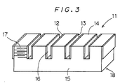
- a capacitor array 11 comprises a plurality of capacitor elements 14, each of which is provided with external electrodes 12 and 13 on both end surfaces thereof. These capacitor elements 14 are held by a carrier part 15 in common, with spaces 16 defined therebetween.
- Each of the capacitor element 14 forms a multilayer capacitor comprising a plurality of internal electrodes 17, as shown expediently in the leftmost one appearing in Fig. 3. Actually, the internal electrodes 17 are not visible from the outside.
- a block 18 is prepared for providing the capacitor elements 14 and the carrier part 15. In this stage, the block 18 is not yet provided with grooves corresponding to the spaces 16.
- This block 18 is formed by a layered product of a plurality of ceramic green sheets, which are provided with the internal electrodes 17 on desired positions.
- grooves for defining the spaces 16 are formed in the block 18, not to reach the carrier part 15.
- metal paste for forming the external electrodes 12 and 13 is applied into the aforementioned grooves.
- the metal paste filling up each groove is dried and then cut to be divided in two.
Landscapes
- Engineering & Computer Science (AREA)
- Power Engineering (AREA)
- Manufacturing & Machinery (AREA)
- Microelectronics & Electronic Packaging (AREA)
- Ceramic Capacitors (AREA)
- Fixed Capacitors And Capacitor Manufacturing Machines (AREA)
- Apparatuses And Processes For Manufacturing Resistors (AREA)
Claims (11)
- Verfahren zum Herstellen mehrerer elektronischer Bauteile zum Aufbringen einer Außenelektrode an mindestens einer Endseite jedes Bauteils, mit den folgenden Schritten:- Herstellen eines Blocks (1, 1a), der die mehreren elektronischen Bauteile enthält;- Einschneiden einer Nut (5) oder mehrerer in den Block (1, 1a), um die mehreren Bauteile voneinander zu trennen und um an jedem Bauteil die genannte mindestens eine Endseite (3, 4) zu erzeugen, die mit Außenelektroden zu versehen ist;- Einbringen von Metallpaste (7) in die Nut (5) oder die mehreren und- Zerschneiden der jede Nut (5) auffüllenden Metallpaste (7), um dieselbe zweizuteilen und dadurch an der mindestens einen genannten Endseite (3, 4) jeder der Bauteile eine Außenelektrode auszubilden, die aus einem Metallpastefilm gewünschter Dicke besteht.
- Verfahren zum Herstellen mehrerer elektronischer Bauteile gemäß Anspruch 1, bei dem die elektronischen Bauteile chipförmige, keramische Elektronikbauteile sind und der Block (1, 1a) aus ungebranntem Keramikmaterial besteht, wobei das Verfahren ferner einen Schritt des gemeinsamen Brennens der Metallpaste (7) und des ungebrannten Keramikmaterials nach dem Schritt des Zertrennens der Metallpaste (7) aufweist.
- Verfahren zum Herstellen elektronischer Chipbauteile gemäß Anspruch 1, bei dem die elektronischen Chipbauteile chipförmige, keramische Elektronikbauteile sind und der Block (1, 1a) aus ungebranntem Keramikmaterial besteht, wobei das Verfahren ferner einen Schritt des Brennens des ungebrannten Keramikmaterials vor dem Schritt des Einschneidens der Nuten (5) in den Block enthält.
- Verfahren zum Herstellen chipförmiger Elektronikbauteile nach einem der vorstehenden Ansprüche, bei dem der Schritt des Einschneidens der Nuten (5) in den Block (1, 1a) mit einer Trennsäge ausgeführt wird.
- Verfahren zum Herstellen elektronischer Chipbauteile nach Anspruch 1, ferner mit einem Schritt des Trocknens der Metallpaste (7) zwischen dem Schritt des Auftragens der Metallpaste (7) und dem Schritt des Durchschneidens der Metallpaste (7).
- Verfahren zum Herstellen elektronischer Chipbauteile nach Anspruch 1, ferner mit einem Schritt des Bereitstellens einer ersten Schneide zum Einschneiden der Nuten (5) in den Block (1, 1a) und einer zweiten Schneide (8) zum Durchschneiden der Metallpaste (7), und mit einem Schritt des Auswählens der Dickendifferenz zwischen der ersten und der zweiten Schneide, um die Dicken der herzustellenden Außenelektroden festzulegen.
- Verfahren zum Herstellen elektronischer Bauteile nach Anspruch 1, bei dem der Block (1a) entlang mehrerer zueinander rechtwinkliger Schnittlinien (9, 10) zerteilt wird, um mehrere elektronische Chipbauteile zu erzeugen, und bei dem die Nuten (5) entlang der ersten Schnittlinien (9) eingeschnitten werden, wobei das Verfahren ferner einen Schritt des Zertrennens des Blocks (la) entlang der zweiten Schnittlinien (10) enthält.
- Verfahren zum Herstellen eines Arrays aus elektronischen Bauteilen (11) mit mehreren elektronischen Bauteilen (14), die jeweils an zwei Enden mit Außenelektroden (12, 13) versehen sind, und mit einem Trägerteil (15), das diese elektronischen Komponenten (14) gemeinsam hält, wobei Zwischenräume (16) zwischen diesen liegen, mit den folgenden Schritten:- Herstellen eines Blocks (18), der die elektronischen Bauteile (14) und den Trägerteil (15) enthält;- Einschneiden von Nuten in den Block (18) zwischen den elektronischen Bauteilen in solcher Weise, daß sie sich nicht in den Trägerteil (15) erstrecken, um an den elektronischen Bauteilen Seiten auszubilden, die mit Außenelektroden (12, 13) zu versehen sind;- Einbringen von Metallpaste in die Nuten und- Zerschneiden der jede Nut auffüllenden Metallpaste, um dieselbe zweizuteilen und dadurch an den Seiten der elektronischen Bauteile eine Außenelektrode auszubilden, die aus einem Metallpastefilm gewünschter Dicke besteht.
- Verfahren zum Herstellen eines Arrays aus elektronischen Bauteilen nach Anspruch 8, bei dem jedes der elektronischen Bauteile einen Kondensator bildet.
- Verfahren zum Herstellen eines Arrays elektronischer Bauteile nach Anspruch 8, bei dem der Block (18) aus einem ungebrannten Keramikmaterial besteht und das Verfahren ferner einen Schritt des gemeinsamen Trennens der Metallpaste und des ungebrannten Keramikmaterials nach dem Schritt des Durchschneidens der Metallpaste umfaßt.
- Verfahren zum Herstellen eines Arrays aus elektronischen Bauteilen nach Anspruch 8, bei dem der Block (18) aus einem ungebrannten Keramikmaterial besteht und das Verfahren ferner einen Schritt des Brennens des ungebrannten Keramikmaterials vor dem Schritt des Herstellens der Nuten umfaßt.
Applications Claiming Priority (2)
| Application Number | Priority Date | Filing Date | Title |
|---|---|---|---|
| JP255640/91 | 1991-10-03 | ||
| JP3255640A JP3018645B2 (ja) | 1991-10-03 | 1991-10-03 | チップ部品の製造方法 |
Publications (3)
| Publication Number | Publication Date |
|---|---|
| EP0535995A2 EP0535995A2 (de) | 1993-04-07 |
| EP0535995A3 EP0535995A3 (en) | 1993-05-12 |
| EP0535995B1 true EP0535995B1 (de) | 1995-08-09 |
Family
ID=17281557
Family Applications (1)
| Application Number | Title | Priority Date | Filing Date |
|---|---|---|---|
| EP92309050A Expired - Lifetime EP0535995B1 (de) | 1991-10-03 | 1992-10-05 | Herstellungsverfahren von elektronischen Komponenten |
Country Status (4)
| Country | Link |
|---|---|
| US (1) | US5295289A (de) |
| EP (1) | EP0535995B1 (de) |
| JP (1) | JP3018645B2 (de) |
| DE (1) | DE69204005T2 (de) |
Families Citing this family (18)
| Publication number | Priority date | Publication date | Assignee | Title |
|---|---|---|---|---|
| US5583738A (en) * | 1993-03-29 | 1996-12-10 | Murata Manufacturing Co., Ltd. | Capacitor array |
| JP2870371B2 (ja) * | 1993-08-05 | 1999-03-17 | 株式会社村田製作所 | 積層電子部品、その製造方法およびその特性測定方法 |
| JP3524630B2 (ja) * | 1995-04-07 | 2004-05-10 | Fdk株式会社 | 積層誘電体フィルタ及びその製造方法 |
| DE69603931T2 (de) * | 1995-06-27 | 2000-03-30 | Koninkl Philips Electronics Nv | Methode zur herstellung von mehrlagigen elektronischen komponenten |
| US5880011A (en) * | 1996-06-19 | 1999-03-09 | Pacific Trinetics Corporation | Method and apparatus for manufacturing pre-terminated chips |
| JP2001502123A (ja) * | 1997-08-05 | 2001-02-13 | コーニンクレッカ フィリップス エレクトロニクス エヌ ヴィ | 複数の電子部品の製造方法 |
| US6678927B1 (en) * | 1997-11-24 | 2004-01-20 | Avx Corporation | Miniature surface mount capacitor and method of making same |
| GB9817120D0 (en) * | 1998-08-07 | 1998-10-07 | Abb Power T & D Limited | Improvements in or relating to electronic components |
| US6515842B1 (en) | 2000-03-30 | 2003-02-04 | Avx Corporation | Multiple array and method of making a multiple array |
| JP3882718B2 (ja) * | 2002-08-29 | 2007-02-21 | 株式会社村田製作所 | 薄膜積層電子部品の製造方法 |
| DE102005016590A1 (de) * | 2005-04-11 | 2006-10-26 | Epcos Ag | Elektrisches Mehrschicht-Bauelement und Verfahren zur Herstellung eines Mehrschicht-Bauelements |
| JP4730559B2 (ja) * | 2006-12-26 | 2011-07-20 | Tdk株式会社 | 電子部品及びその製造方法 |
| KR101498098B1 (ko) * | 2009-07-01 | 2015-03-03 | 케메트 일렉트로닉스 코포레이션 | 고전압 성능을 가지는 고캐패시턴스 다층레이어 |
| KR101141402B1 (ko) | 2011-03-09 | 2012-05-03 | 삼성전기주식회사 | 적층 세라믹 커패시터 및 그 제조방법 |
| JP2014187216A (ja) * | 2013-03-23 | 2014-10-02 | Kyocera Corp | 積層セラミックコンデンサの製造方法 |
| US11443898B2 (en) * | 2017-04-10 | 2022-09-13 | Presidio Components. Inc. | Multilayer broadband ceramic capacitor with internal air gap capacitance |
| DE112020001211T5 (de) * | 2019-03-12 | 2021-12-02 | Tdk Corporation | Laminierte Festkörper-Sekundärzelle und Verfahren zur Herstellung derselben |
| JP7188345B2 (ja) * | 2019-09-30 | 2022-12-13 | 株式会社村田製作所 | 積層セラミック電子部品の製造方法 |
Family Cites Families (3)
| Publication number | Priority date | Publication date | Assignee | Title |
|---|---|---|---|---|
| JPS60109204A (ja) * | 1983-11-17 | 1985-06-14 | 株式会社村田製作所 | チップ部品の外部電極形成方法 |
| JPH01225307A (ja) * | 1988-03-05 | 1989-09-08 | Murata Mfg Co Ltd | 積層セラミックコンデンサの製造方法 |
| JPH03225904A (ja) * | 1990-01-31 | 1991-10-04 | Taiyo Yuden Co Ltd | 積層チップへの導電ペースト塗布方法 |
-
1991
- 1991-10-03 JP JP3255640A patent/JP3018645B2/ja not_active Expired - Lifetime
-
1992
- 1992-10-02 US US07/955,838 patent/US5295289A/en not_active Expired - Lifetime
- 1992-10-05 EP EP92309050A patent/EP0535995B1/de not_active Expired - Lifetime
- 1992-10-05 DE DE69204005T patent/DE69204005T2/de not_active Expired - Lifetime
Also Published As
| Publication number | Publication date |
|---|---|
| JPH05101996A (ja) | 1993-04-23 |
| EP0535995A2 (de) | 1993-04-07 |
| US5295289A (en) | 1994-03-22 |
| DE69204005D1 (de) | 1995-09-14 |
| JP3018645B2 (ja) | 2000-03-13 |
| EP0535995A3 (en) | 1993-05-12 |
| DE69204005T2 (de) | 1996-03-07 |
Similar Documents
| Publication | Publication Date | Title |
|---|---|---|
| EP0535995B1 (de) | Herstellungsverfahren von elektronischen Komponenten | |
| US10714261B2 (en) | Multilayer ceramic capacitor | |
| US4852227A (en) | Method for making a multilayer ceramic capacitor with buried electrodes and terminations at a castellated edge | |
| US5692280A (en) | Manufacturing method of laminated ceramic electronic components | |
| JPH10241991A (ja) | 積層コンデンサとそのトリミング方法 | |
| US7926154B2 (en) | Method of manufacturing multi-layer ceramic condenser | |
| JPH07122455A (ja) | セラミック積層電子部品の製造方法 | |
| JP4099756B2 (ja) | 積層基板 | |
| KR100676035B1 (ko) | 적층 세라믹 콘덴서 | |
| JPH09260187A (ja) | セラミック電子部品の製造方法 | |
| JPH10144504A (ja) | チップ型サーミスタ及びその製造方法 | |
| US6846375B2 (en) | Method of manufacturing multilayer ceramic wiring board and conductive paste for use | |
| JP2000269074A (ja) | 積層セラミックコンデンサとその製造方法 | |
| JPH0917607A (ja) | チップ状回路部品とその製造方法 | |
| JP3493812B2 (ja) | セラミック電子部品の製造方法 | |
| JPH1092606A (ja) | チップ型サーミスタ及びその製造方法 | |
| JPH09260105A (ja) | チップ型サーミスタ及びその製造方法 | |
| US11515090B2 (en) | Ceramic electronic component and method for manufacturing ceramic electronic component | |
| JPH0945830A (ja) | チップ状電子部品 | |
| JPH08321406A (ja) | 積層型複合素子及びその製造方法 | |
| JPH06283335A (ja) | チップインダクタ及びその製造方法 | |
| JPH08273972A (ja) | 電子部品の製造方法 | |
| JPH1126279A (ja) | 積層セラミック電子部品の製造方法 | |
| JP3158793B2 (ja) | コンデンサアレイ | |
| JP2004022958A (ja) | 多数個取りセラミック基板 |
Legal Events
| Date | Code | Title | Description |
|---|---|---|---|
| PUAI | Public reference made under article 153(3) epc to a published international application that has entered the european phase |
Free format text: ORIGINAL CODE: 0009012 |
|
| PUAL | Search report despatched |
Free format text: ORIGINAL CODE: 0009013 |
|
| AK | Designated contracting states |
Kind code of ref document: A2 Designated state(s): DE FR GB |
|
| AK | Designated contracting states |
Kind code of ref document: A3 Designated state(s): DE FR GB |
|
| 17P | Request for examination filed |
Effective date: 19930621 |
|
| 16A | New documents despatched to applicant after publication of the search report | ||
| 17Q | First examination report despatched |
Effective date: 19940218 |
|
| GRAA | (expected) grant |
Free format text: ORIGINAL CODE: 0009210 |
|
| AK | Designated contracting states |
Kind code of ref document: B1 Designated state(s): DE FR GB |
|
| REF | Corresponds to: |
Ref document number: 69204005 Country of ref document: DE Date of ref document: 19950914 |
|
| ET | Fr: translation filed | ||
| PLBE | No opposition filed within time limit |
Free format text: ORIGINAL CODE: 0009261 |
|
| STAA | Information on the status of an ep patent application or granted ep patent |
Free format text: STATUS: NO OPPOSITION FILED WITHIN TIME LIMIT |
|
| 26N | No opposition filed | ||
| REG | Reference to a national code |
Ref country code: GB Ref legal event code: IF02 |
|
| PGFP | Annual fee paid to national office [announced via postgrant information from national office to epo] |
Ref country code: GB Payment date: 20100929 Year of fee payment: 19 |
|
| PGFP | Annual fee paid to national office [announced via postgrant information from national office to epo] |
Ref country code: DE Payment date: 20100929 Year of fee payment: 19 |
|
| PGFP | Annual fee paid to national office [announced via postgrant information from national office to epo] |
Ref country code: FR Payment date: 20111103 Year of fee payment: 20 |
|
| REG | Reference to a national code |
Ref country code: DE Ref legal event code: R071 Ref document number: 69204005 Country of ref document: DE |
|
| REG | Reference to a national code |
Ref country code: DE Ref legal event code: R071 Ref document number: 69204005 Country of ref document: DE |
|
| REG | Reference to a national code |
Ref country code: GB Ref legal event code: PE20 Expiry date: 20121004 |
|
| PG25 | Lapsed in a contracting state [announced via postgrant information from national office to epo] |
Ref country code: GB Free format text: LAPSE BECAUSE OF EXPIRATION OF PROTECTION Effective date: 20121004 |