EP0502382A1 - Composition photosensible et procédé - Google Patents
Composition photosensible et procédé Download PDFInfo
- Publication number
- EP0502382A1 EP0502382A1 EP92102959A EP92102959A EP0502382A1 EP 0502382 A1 EP0502382 A1 EP 0502382A1 EP 92102959 A EP92102959 A EP 92102959A EP 92102959 A EP92102959 A EP 92102959A EP 0502382 A1 EP0502382 A1 EP 0502382A1
- Authority
- EP
- European Patent Office
- Prior art keywords
- composition
- resin
- compound
- phenolic resin
- epoxy
- Prior art date
- Legal status (The legal status is an assumption and is not a legal conclusion. Google has not performed a legal analysis and makes no representation as to the accuracy of the status listed.)
- Withdrawn
Links
Images
Classifications
-
- G—PHYSICS
- G03—PHOTOGRAPHY; CINEMATOGRAPHY; ANALOGOUS TECHNIQUES USING WAVES OTHER THAN OPTICAL WAVES; ELECTROGRAPHY; HOLOGRAPHY
- G03F—PHOTOMECHANICAL PRODUCTION OF TEXTURED OR PATTERNED SURFACES, e.g. FOR PRINTING, FOR PROCESSING OF SEMICONDUCTOR DEVICES; MATERIALS THEREFOR; ORIGINALS THEREFOR; APPARATUS SPECIALLY ADAPTED THEREFOR
- G03F7/00—Photomechanical, e.g. photolithographic, production of textured or patterned surfaces, e.g. printing surfaces; Materials therefor, e.g. comprising photoresists; Apparatus specially adapted therefor
- G03F7/004—Photosensitive materials
- G03F7/04—Chromates
-
- G—PHYSICS
- G03—PHOTOGRAPHY; CINEMATOGRAPHY; ANALOGOUS TECHNIQUES USING WAVES OTHER THAN OPTICAL WAVES; ELECTROGRAPHY; HOLOGRAPHY
- G03F—PHOTOMECHANICAL PRODUCTION OF TEXTURED OR PATTERNED SURFACES, e.g. FOR PRINTING, FOR PROCESSING OF SEMICONDUCTOR DEVICES; MATERIALS THEREFOR; ORIGINALS THEREFOR; APPARATUS SPECIALLY ADAPTED THEREFOR
- G03F7/00—Photomechanical, e.g. photolithographic, production of textured or patterned surfaces, e.g. printing surfaces; Materials therefor, e.g. comprising photoresists; Apparatus specially adapted therefor
- G03F7/004—Photosensitive materials
- G03F7/038—Macromolecular compounds which are rendered insoluble or differentially wettable
-
- H—ELECTRICITY
- H05—ELECTRIC TECHNIQUES NOT OTHERWISE PROVIDED FOR
- H05K—PRINTED CIRCUITS; CASINGS OR CONSTRUCTIONAL DETAILS OF ELECTRIC APPARATUS; MANUFACTURE OF ASSEMBLAGES OF ELECTRICAL COMPONENTS
- H05K3/00—Apparatus or processes for manufacturing printed circuits
- H05K3/22—Secondary treatment of printed circuits
- H05K3/28—Applying non-metallic protective coatings
- H05K3/285—Permanent coating compositions
- H05K3/287—Photosensitive compositions
-
- Y—GENERAL TAGGING OF NEW TECHNOLOGICAL DEVELOPMENTS; GENERAL TAGGING OF CROSS-SECTIONAL TECHNOLOGIES SPANNING OVER SEVERAL SECTIONS OF THE IPC; TECHNICAL SUBJECTS COVERED BY FORMER USPC CROSS-REFERENCE ART COLLECTIONS [XRACs] AND DIGESTS
- Y10—TECHNICAL SUBJECTS COVERED BY FORMER USPC
- Y10S—TECHNICAL SUBJECTS COVERED BY FORMER USPC CROSS-REFERENCE ART COLLECTIONS [XRACs] AND DIGESTS
- Y10S430/00—Radiation imagery chemistry: process, composition, or product thereof
- Y10S430/136—Coating process making radiation sensitive element
Definitions
- This invention relates to light-sensitive compositions. More particularly, this invention relates to aqueous developable light-sensitive compositions useful as high resolution soldermasks in the manufacture of printed circuit boards.
- Aqueous developable liquid soldermasks are known. They are typically applied as a wet coating, such as by curtain coating, dried, image-wise exposed to activating radiation, partially cured using heat, developed, such as with an aqueous alkaline solution, and often finally cured. Examples of aqueous developable soldermasks are disclosed in European patent Publication No. 0,255,989 and in Japanese published Patent Disclosures 55-129341 and 60-26943 published October 7, 1980 and February 9, 1985, respectively.
- Soldermasks disclosed in these publications typically consist of at least one alkali soluble phenolic resin, a compound containing at least two epoxy or vinyl ether groups, generally an epoxy resin, and a photoactive component such as a sulfonium salt or an azide compound capable of initiating crosslinking of the epoxy or vinyl ether compound upon exposure to activating radiation with heating as necessary.
- a photoactive component such as a sulfonium salt or an azide compound capable of initiating crosslinking of the epoxy or vinyl ether compound upon exposure to activating radiation with heating as necessary.
- the phenolic component in adequate concentration, enables aqueous development, and the combination of the epoxy or vinyl ether compound and the photoactive component permits cure in exposed areas of the film.
- aqueous developable soldermasks fail to yield a high resolution image upon development. It is believed that a cause of poor resolution is the phenolic component of the formulation. Prior to development, the phenolic component is essentially uncured because the liberation of acid by the photoreaction does not catalyze curing of the phenolic component of the soldermask. Consequently, upon contact of an exposed film with developer, selective development is possible between exposed and non-exposed areas because the epoxy or vinyl ether component is cured, but high resolution images are not obtained because the phenolic component is non-selectively dissolved from both exposed and non-exposed portions of the coating alike.
- thermo curing agent for the phenolic component may be included in the formulation.
- the phenolic of the composition cannot be cured prior to development because curing will take place uniformly in both exposed and non-exposed portions of the film making development difficult or impossible. Therefore, inclusion of a thermal curing agent would not overcome the problem of poor resolution following development.
- the photoimageable composition of the invention comprises a binder that is a mixture comprising an alkali soluble phenolic resin and a compound containing at least two active groups selected from epoxy groups, vinyl ether groups and mixtures of the two, a photoactive compound that liberates a curing catalyst for binder components in imaged areas upon patterned exposure to activating radiation, and a crosslinking agent for the phenolic resin component of the binder that is activated in the presence of a photogenerated curing catalyst.
- the primary components of the binder comprise a poly(vinyl phenol) and an epoxy resin.
- the composition of the invention is used in conventional manner. It is applied to a substrate, dried, exposed to patterned radiation at a wavelength that causes a photoreaction that liberates a curing catalyst, heated as necessary to cure the film in exposed areas, developed and optionally heat cured.
- all primary components of the binder, inclusive of the phenolic component are cured in imaged areas, but not elsewhere. Therefore, upon development, high resolution images are obtained because uncured binder is essentially not solvated in the exposed areas of the film.
- a post development bake step may be employed to complete the curing reactions.
- the drawing is a diagrammatic representation of comparative processes and results using a photoactivated curing agent for all polymer components in accordance with the invention compared to results that would be obtained using a non-photoactive curing agent for the binder components.
- the phenolic resin component of the composition of the invention is a film-forming resin having phenolic hydroxyl groups that permit development of the composition in an aqueous alkaline developer.
- Phenolic resins are well known in the art.
- Exemplary phenolic resins include, for example, phenol aldehyde condensates known as the novolak resins, homo and copolymers of alkenyl phenols and homo and copolymers of N-hydroxyphenylmaleimides.
- Novolak resins are preferred. They are made following procedures known in the art and disclosed in numerous publications such as by DeForest, Photoresist Materials and Processes , McGraw-Hill Book Company, New York, Ch. 2, 1975 and by Moreau, Semiconductor Lithography Principles, Practices and Materials , Plenum Press, New York, Chs. 2 and 4, 1988, both incorporated herein by reference. Novolak resins are the thermoplastic condensation product of a phenol and an aldehyde.
- Suitable phenols for condensation with an aldehyde, especially formaldehyde, for the formation of novolak resins include phenol; m-cresol; o-cresol; p-cresol; 2,4-xylenol; 2,5-xylenol; 3,4-xylenol; 3,5-xylenol; thymol and mixtures thereof.
- An acid catalyzed condensation reaction results in the formation of a suitable novolak resin which may vary in molecular weight from about 500 to 100,000 daltons.
- the preferred novolak resins are the cresol formaldehyde condensation products.
- Poly(vinyl phenol) resins may be formed by block polymerization, emulsion polymerization or solution polymerization of corresponding monomers in the presence of a suitable catalyst.
- Suitable materials for purposes of the invention, include those materials disclosed in EPO application publication No. 0,255,989 and in U.S. Patent No. 4,439,516 incorporated herein by reference.
- phenolic resins for purposes of the present invention, include homo and copolymers of N-hydroxyphenyl maleimides. Such materials are also disclosed in the above-cited European published application 0,255,989 beginning on page 2, line 45 and continuing to page 5, line 51, incorporated herein by reference for its teaching of such resins.
- phenolic resin as used herein are the copolymers of cyclic alcohols and phenols as disclosed in published European patent application No. 0 401 499 having a publication date of December 12, 1990 and incorporated herein by reference.
- Another component of the composition of the invention is one containing at least two active groups selected from epoxy groups, vinyl ether groups and mixtures of the two.
- Useful epoxy-containing materials are disclosed in the above referenced EPO application publication No. 0,255,989. They may vary from low molecular weight monomeric materials to high molecular weight polymers and may vary greatly in the nature of their backbone and substituent groups.
- the backbone may be of any type and substituent groups may be any group free of an active hydrogen atom reactive with an oxirane ring at room temperature.
- suitable substituents include halogens, ester groups, ethers, sulfonate groups, siloxane groups, nitro groups, phosphate groups, etc.
- Exemplary epoxy-containing materials include glycidyl ethers such as the glycidyl ethers of polyhydric phenols obtained by reacting a polyhydric phenol with an excess of chlorohydrin such as epichlorohydrin. Further examples of epoxy materials of this type are described in U.S. Patent No. 3,018,262, incorporated herein by reference.
- epoxy materials suitable for use in the compositions of the invention.
- Such materials include epichlorohydrin, glycidol, glycidylmethacrylate, the glycidyl ether of p-tertiarybutylphenol (e.g. those available under the trade designation “Epi-Rez” 5014 from Celanese); diglycidyl ether of Bisphenol A (e.g. those available under the trade designations "Epon 828,” “Epon 1004" and “Epon 1010” from Shell Chemical Co. and "DER-331,” “DER-332” and “DER-334,” from Dow Chemical Co.), vinylcyclohexene dioxide (e.g.
- ERP-4206 from Union Carbide Corp.
- 3,4-epoxy-6-methylcyclohexylmethyl-3,4-epoxy-6-methylcyclohexene carboxylate e.g. "ERL-4201” from Union Carbide Corp.
- bis(2,3-epoxycyclopentyl) ether e.g. "ERL-0400” from Union Carbide Corp.
- aliphatic epoxy modified with polypropylene glycol e.g. "ERL-4050” and “ERL-4052” from Union Carbide Corp.
- epoxidized polybutadiene e.g. "Oxiron 2001” from FMC Corp.
- flame retardant epoxy resins e.g.
- DER-580 a brominated bisphenol type epoxy resin available from Dow Chemical Co.
- 1,4-butanediol diglycidyl ether of phenol formaldehyde novolak e.g. "DEN-431” and “DEN-438” from Dow Chemical co.
- resorcinol diglycidyl ether e.g. "Kopoxite” from Koppers Company, Inc.
- Examples of compounds with at least two vinyl ether groups include divinyl ethers of aliphatic, cycloaliphatic, aromatic or araliphatic diols.
- examples of such materials include divinyl ethers of aliphatic diols having from 1 to 12 carbon atoms, polyethylene glycols, propylene glycols, polybutylene glycols, dimethylcyclohexanes, etc.
- Specific examples include divinyl ethers of ethylene glycol, trimethylene-1,3- diol, diethylene glycol, triethylene glycol, dipropylene glycol, tripropylene glycol, resorcinol, Bisphenol A, etc.
- the photoactive compound used in the composition of the invention is one that liberates a photogenerated curing catalyst upon exposure to activating radiation.
- the catalyst is an acid.
- the photogenerated curing catalyst initiates the reactions that cause cure of the binder components in the presence of curing agents, as necessary. Since the curing reactions are dependent upon a photogenerated catalyst, curing takes place only in exposed areas of a coating formed from the composition. Since all primary components of the binder are cured in the exposed coating, differential solubility between exposed areas and unexposed areas is excellent resulting in developed images of high resolution without significant loss of binder from exposed areas.
- photoacid generators useful in the compositions of the invention are known in the art and extensively described in the literature such as in U.S. Patents Nos. 4,090,936 and 5,034,304 incorporated herein by reference.
- One class of preferred acid generators are onium salts of a Group VA element, onium salts of a Group VI A element, and aromatic halonium salts. These complex salts, upon being exposed to activating radiation such as ultraviolet radiation or electron beam irradiation, generate acids capable of initiating the required reactions.
- Preferred onium photoactive compounds are aromatic iodonium complex salts and aromatic sulfonium complex salts. These materials are fully disclosed in the above noted published EPO application No. 0,255,989.
- aromatic iodonium complex salt photoactive compounds include diphenyliodonium tetrafluoroborate, diphenyliodonium hexafluorophosphate, phenyl-2-thienyliodonium hexafluorophosphate, diphenyliodonium hexafluoroantimonate, di(2,4-dichlorophenyl)iodonium hexafluorophosphate, di(4-methoxyphenyl)iodonium hexafluorophosphate and di(3-methoxycarbonylphenyl)iodonium hexafluorophosphate, di(4-acetamidophenyl)iodonium hexafluorophosphate.
- aromatic sulfonium compounds include triphenylsulfonium tetrafluoroborate, dimethylphenylsulfonium hexafluorophosphate, tritolysulfonium hexafluorophosphate, 4-butoxyphenyldiphenylsulfonium tetrafluoroborate, tris(4-phenoxyphenyl)sulfonium hexafluorophosphate, 4-acetoxy-phenyldiphenylsulfonium tetrafluoroborate, tris(4-thiomethoxyphenyl)sulfonium hexafluorophosphate, di(methoxynaphthyl)methylsulfonium tetrafluoroborate, dimethylnaphthylsulfonium hexafluorophosphate and phenylmethylbenxylsulfonium hexafluorophosphate.
- triaryl substituted salts such as triphenylsulfonium hexafluorophosphate are preferred.
- photoactive compounds suitable for purposes of the present invention are the photoacid generators such as those disclosed in U.S. Patent No. 5,034,304.
- halogenated photoacid generators are preferred. These materials include 1,10-dibromodecane; 1,1-bis[p-chlorophenyl]-2,2-di-dichloroethane; 4,41-dichloro-2-(trichloromethyl) benzhydrol or 1,1-bis(chlorophenyl)2-2,2-trichloroethane (Kelthane R ); hexachlorodimethyl sulfone; 2-chloro-6-(trichloromethyl) pyridine; 0,0-diethyl-0-(3,5,6-trichloro-2-pyridyl)phosporothionate (Dursban R ); 1,2,3,4,5,6-hexachlorocyclohexane; N(1,1-bis [p-chlorophenyl]-2,2,2-
- An additional component of the composition of this invention is a low temperature curing agent for the phenolic component of the binder catalyzed by photogenerated catalyst.
- Preferred curing agents are acid catalyzed materials reactive with the phenolic hydroxyl group.
- An especially preferred agent is a melamine formaldehyde resin.
- Melamine formaldehyde resins are amino resins formed by condensation of formaldehyde with melamine.
- the resins are typically ethers such as trialkylol melamine and hexaalkylol melamine.
- the alkyl group may have from 1 to as many as 8 or more carbon atoms but is preferably methyl. Dependent upon the reaction conditions and the concentration of formaldehyde, the methyl ethers may react with each other to form more complex units.
- the preferred melamine formaldehyde resin has a degree of polymerization varying between 1.3 and 2.0 and most preferably, is a member of the Cymel 300 Resin series which are highly methylated melamine formaldehyde resins.
- the most preferred melamine formaldehyde resin for purposes of this invention is Cymel 301 which is a hexamethoxymethyl melamine with a low methylol content having alkoxy groups as the principle reactive groups and a degree of polymerization of 1.5.
- the preferred catalyzed crosslinking agents are believed to react primarily with the phenolic resin. Consequently, it is believed that the following exposure and low temperature cure and prior to development, the photoimaged composition in exposed portions of the film comprise a network consisting primarily of epoxy condensation products and the reaction product of the phenolic resin and the melamine resin.
- Sensitizers constitute a preferred additive and are added to increase the range of wavelength photosensitivity.
- Suitable sensitizers include phenothiazines inclusive of substituted phenothiazines, 2-ethyl-9,10-dimethoxy-anthracene, 9,10-dichloroanthracene, 9,10-phenylanthracene, 1-chloroanthracene, 2-methylanthracene, 9-methylanthracene, 2-t-butyl anthracene, anthracene, 1,2-benzanthracene, 1,2,3,4-dibenzanthracene, 1,2,5,6-dibenzanthracene, 1,2,7,8-dibenzanthracene, 9,10-dimethoxydimethylanthracene, and the like.
- a suitable solvent such as, for example, one or more glycol ethers such as ethylene glycol monomethyl ether, ethylene glycol monoethyl ether; esters such as a methyl cellosolve acetate, ethyl cellosolve acetate, propylene glycol monomethyl ether acetate, dipropylene glycol monomethyl ether acetate and other solvents such as dibasic esters, propylene carbonate and gamma-butaryl lactone.
- glycol ethers such as ethylene glycol monomethyl ether, ethylene glycol monoethyl ether
- esters such as a methyl cellosolve acetate, ethyl cellosolve acetate, propylene glycol monomethyl ether acetate, dipropylene glycol monomethyl ether acetate
- other solvents such as dibasic esters, propylene carbonate and gamma-butaryl lactone.
- composition components may vary within wide limits dependent upon the use of the material. Concentration ranges for the principal ingredients of the formulation are set forth in the following table and expressed as dry solids in parts by weight. Broad Range Preferred Range Phenolic Resin 25 - 65 40 - 50 Epoxy or Vinyl Compound 15 - 50 25 - 35 Crosslinking Agent 5 - 35 1 - 20 Photoactive Compound 1 - 15 2 - 10
- additives commonly found in such compositions are present in minor concentration except for fillers and pigments which may be present in larger concentration such as, for example, in amounts of from 5 to 30 percent by weight of the total of the dry components.
- the above components are desirably dispersed in a solvent to form a liquid coating composition.
- Their concentration in a solvent would depend on several factors, for example, the coating method used to apply the material to a substrate.
- the concentration of the dry components in a slot coating composition would be higher than in a curtain coating composition.
- the concentration of the dry components in the solvent may vary from about 10 to 50 weight percent or more of the total weight of the coating composition.
- the percentage may vary between about 20 and 30 percent of the total concentration
- for slot coating may vary between 40 and 50 percent, it being understood that the weight percentage of solids in the composition would be best determined by the viscosity required for the particular coating method used. If the composition is to be applied as a dry film, of course the dry film would be essentially free of solvent.
- the coating composition of the invention is used in conventional manner provided there is a step of low temperature cure following exposure and preceding development.
- the photoimageable composition may be applied to a substrate having a pattern of conductive material disposed thereon.
- the substrate may be a copper laminate substrate prepared by the method described in the second chapter of Printed Circuits Handbook by Clyde F. Coombs, Jr., 2nd Edition, McGraw-Hill, 1979.
- Other suitable substrates include those prepared by laminating multilayer boards for the manufacture of printed circuit boards with vias (through-holes) and interconnections which may contain solder, as described in chapter twenty-three of the above reference, both incorporated herein by reference.
- the composition of the invention is coated onto the substrate using conventional techniques and preferably, the coating is deposited so as to yield a dry film thickness of at least 0.50 mil on top of a trace as required by IPC Specification No. SM-840B.
- the wet film formed is dried at a temperature varying between about 80 and 100 o C for a time of from about 20 to 60 minutes to remove solvent. During this drying step, it is desirable to avoid temperatures in excess of 120 o C and drying times of more than 60 minutes to prevent premature curing of the composition as this could make development difficult.
- the process of transferring an image to the coating involves exposing the coating to a source of patterned activating radiation to initiate the photoreaction in exposed areas. Suitable sources of activating radiation include actinic radiation, x-rays, etc.
- Suitable sources of activating radiation include actinic radiation, x-rays, etc.
- the layer is subjected to a low temperature bake to initiate crosslinking of the exposed portions of the binder by the liberation of the photogenerated catalyst.
- the bake conditions comprise heating to a temperature capable of initiating the curing reaction but the temperature should be below that temperature where thermal crosslinking would occur in unexposed areas of the film.
- the bake temperature varies between about 85 to 120 o C and the bake time ranges between 1 and 20 minutes.
- catalyst generated by the photoreaction initiates the curing reaction of the binder components in exposed areas of the film.
- the area not exposed to activating radiation and free of photogenerated catalyst remains uncured and is readily dissolved by aqueous alkali solutions such as sodium hydroxide, sodium metasilicate, sodium carbonate, potassium hydroxide, potassium carbonate, ethylene diamine and the like.
- the preferred developer is a metal hydroxide with concentrations between 0.5 to 5% of alkaline hydroxide in water.
- a typical development time is 30 to 60 seconds.
- the remainder of the coating is characterized by a partial cure whereby most of the binder components are crosslinked.
- a second cure is desirable to achieve full thermal and electrical solder mask properties. This may be achieved by heating to a temperature of about 120 to 160 o C for a period of time of between about 10 and 60 minutes. The second cure hardens the developed image and the coating is resistant to soldering and may also be used as a permanent dielectric coating.
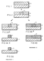
- step 1 substrate 1 is coated with soldermask coating 2.
- Exposure of soldermask coating 2 in step 2 results in a region 3 of the coating having photogenerated acid in exposed areas as represented by the symbol H+.
- step 3A following low temperature cure, coating 2 is cured in region 3 to crosslink the exposed areas of the coating.
- the coating is developed to remove unexposed areas of the coating with exposed and cured region 3 remaining due to decreased solubility in the developer following cure. This is illustrated by Step 4A of the drawing.
- step 5A the crosslinking density in region 3 is significantly increased.
- compositions were prepared by customary mixing procedures where the phenolic resin used is poly-(p-vinylphenol) (PVP); the epoxy resin is a bisphenol A epoxy; the melamine is hexamethoxymethyl melamine; the photoinitiator (PI) is triphenylsulphonium tetrafluoroantimonate; and the solvents are 100% propylene glycol monomethyl ether acetate (S) or a cosolvent of 50% propylene glycol monomethyl ether acetate and 50% dipropylene glycol monomethyl ether acetate (Co).
- concentration of each component for each example is as set forth in the following table.
- Components were mixed together as specified and additional optional components (i.e. dyes, sensitizer, wetting agent and filler) were added.
- the solvent was added to the solids in a one-to-one weight ratio.
- Precleaned copper clad laminate panels (12" x 12") were coated with each formulation using a draw down technique with a #65 Meier rod and dried for 30 to 40 minutes at 95 o C.
- the boards were then exposed using the standard IPC-B25 primary image artwork. After exposure, panels were subjected to a first cure by heating for about 15 minutes at 95 o C. Panels were then developed using an aqueous solution of 15 percent sodium hydroxide. After development, panels were subjected to a second cure by heating at 140 o C for 60 minutes.
- the boards coated with the above compositions were then tested for survival in an alkaline copper plating bath (pH >13) for periods of 7 hours on two consecutive days for a total of 14 hours exposure to the bath.
- the boards were evaluated based on three criteria: adhesion, halo or encroachment, and spots.
- adhesion was measured by counting the squares below the pads on the IPC-B25 pattern. The best results are indicated by the highest number of squares remaining on the board after the test.
- Halo or encroachment was measured at specific locations, indicated by four areas of the IPC pattern, around the edges of a developed image. Halo's are indicative of non-adhesion in those areas and result in unsatisfactory electrical performance of the board. Each of the areas was measured for diameter of the halo and averaged. Because of the spacing between these four areas, a 15 mm encroachment was the worst score.
- Example No. 10 11 12 13 14 15 16 17 18 Component Novolak 50 40 40 45 50 50 45 40 40 Epoxy 50 60 60 55 35 35 40 45 45 Melamine 0 0 0 0 15 15 15 15 P I 4 8 4 8 4 8 6 8 8 Solvent Co S S Co S Co Co Co S
- Results show that the presence of melamine resin in formulations 14 to 18 improves adhesion, significantly reduces the diameter of any halo and reduces the number of spots on the board.
Landscapes
- Physics & Mathematics (AREA)
- General Physics & Mathematics (AREA)
- Spectroscopy & Molecular Physics (AREA)
- Materials For Photolithography (AREA)
- Compositions Of Macromolecular Compounds (AREA)
- Epoxy Resins (AREA)
- Non-Metallic Protective Coatings For Printed Circuits (AREA)
Applications Claiming Priority (4)
| Application Number | Priority Date | Filing Date | Title |
|---|---|---|---|
| US07/663,604 US5206116A (en) | 1991-03-04 | 1991-03-04 | Light-sensitive composition for use as a soldermask and process |
| US663604 | 1992-02-03 | ||
| US07/829,371 US5312715A (en) | 1991-03-04 | 1992-02-03 | Light-sensitive composition and process |
| US829371 | 1997-03-31 |
Publications (1)
| Publication Number | Publication Date |
|---|---|
| EP0502382A1 true EP0502382A1 (fr) | 1992-09-09 |
Family
ID=27098787
Family Applications (1)
| Application Number | Title | Priority Date | Filing Date |
|---|---|---|---|
| EP92102959A Withdrawn EP0502382A1 (fr) | 1991-03-04 | 1992-02-21 | Composition photosensible et procédé |
Country Status (5)
| Country | Link |
|---|---|
| US (1) | US5312715A (fr) |
| EP (1) | EP0502382A1 (fr) |
| JP (1) | JPH05273753A (fr) |
| KR (1) | KR920018521A (fr) |
| DE (1) | DE502382T1 (fr) |
Cited By (3)
| Publication number | Priority date | Publication date | Assignee | Title |
|---|---|---|---|---|
| EP0534204A1 (fr) * | 1991-09-26 | 1993-03-31 | International Business Machines Corporation | Photoréserve de type négatif développable en milieu basique et son emploi |
| US6190833B1 (en) * | 1997-03-30 | 2001-02-20 | Jsr Corporation | Radiation-sensitive resin composition |
| WO2003107093A2 (fr) * | 2002-06-13 | 2003-12-24 | Clariant International Ltd | Composition de photoresist pour lithographie dans l'ultraviolet profond comprenant un melange de composes photo-actifs |
Families Citing this family (13)
| Publication number | Priority date | Publication date | Assignee | Title |
|---|---|---|---|---|
| JP3429852B2 (ja) * | 1993-06-04 | 2003-07-28 | シップレーカンパニー エル エル シー | ネガ型感光性組成物 |
| CA2158915A1 (fr) * | 1994-09-30 | 1996-03-31 | Dekai Loo | Photoresine liquide |
| JPH1041633A (ja) * | 1996-07-25 | 1998-02-13 | Hitachi Ltd | 多層配線板とそれに用いる感光性樹脂組成物 |
| US5858615A (en) * | 1997-07-31 | 1999-01-12 | Morton International, Inc. | Hardenable photoimageable compositions |
| KR100518533B1 (ko) * | 2002-06-14 | 2005-10-04 | 삼성전자주식회사 | 에폭시 링을 포함하는 베이스 폴리머와 실리콘 함유가교제로 이루어지는 네가티브형 레지스트 조성물 및 이를이용한 반도체 소자의 패턴 형성 방법 |
| JP2004206058A (ja) * | 2002-10-31 | 2004-07-22 | Sumitomo Chem Co Ltd | ポジ型感光性組成物 |
| JP4251612B2 (ja) * | 2003-01-30 | 2009-04-08 | ローム・アンド・ハース・エレクトロニック・マテリアルズ,エル.エル.シー. | エポキシ含有物質を含むネガ型感光性樹脂組成物 |
| JP4266310B2 (ja) * | 2003-01-31 | 2009-05-20 | ローム・アンド・ハース・エレクトロニック・マテリアルズ,エル.エル.シー. | 感光性樹脂組成物および該組成物を用いた樹脂パターンの形成方法 |
| JP4397601B2 (ja) * | 2003-02-06 | 2010-01-13 | ローム・アンド・ハース・エレクトロニック・マテリアルズ,エル.エル.シー. | フェノール−ビフェニレン樹脂を含むネガ型感光性樹脂組成物 |
| JP4662793B2 (ja) * | 2005-03-01 | 2011-03-30 | ローム・アンド・ハース・エレクトロニック・マテリアルズ,エル.エル.シー. | エポキシ含有物質を含むネガ型感光性樹脂組成物 |
| JP4633500B2 (ja) * | 2005-03-01 | 2011-02-16 | ローム・アンド・ハース・エレクトロニック・マテリアルズ,エル.エル.シー. | エポキシ含有物質を含むネガ型感光性樹脂組成物 |
| JP4990966B2 (ja) * | 2006-04-13 | 2012-08-01 | コーロン インダストリーズ インク | 金属電極の製造方法 |
| JP6182391B2 (ja) * | 2013-08-21 | 2017-08-16 | ナミックス株式会社 | エポキシ樹脂組成物、感光性樹脂および半導体装置 |
Citations (6)
| Publication number | Priority date | Publication date | Assignee | Title |
|---|---|---|---|---|
| EP0232972A2 (fr) * | 1986-01-13 | 1987-08-19 | Rohm And Haas Company | Composition photoréserve négative et procédé de préparation d'images résistantes à la chaleur utilisant cette composition |
| EP0302019A2 (fr) * | 1987-07-28 | 1989-02-01 | Ciba-Geigy Ag | Photoréserves négatives à base de polyphénols et un choix d'époxydes ou de vinyléthers |
| EP0349803A2 (fr) * | 1988-06-25 | 1990-01-10 | Hoechst Aktiengesellschaft | Mélange réticulable par radiation et matériel pour l'enregistrement sensible aux radiations de ce mélange pour un rayonnement hautement énergétique |
| EP0423446A1 (fr) * | 1989-10-17 | 1991-04-24 | Shipley Company Inc. | Photoréserve pour U.V. proche |
| EP0425418A2 (fr) * | 1989-10-23 | 1991-05-02 | International Business Machines Corporation | PhotorÀ©serve de type négatif développable en milieu basique |
| EP0462391A2 (fr) * | 1990-06-19 | 1991-12-27 | Shipley Company Inc. | Photoréserves durcies par les acides |
Family Cites Families (4)
| Publication number | Priority date | Publication date | Assignee | Title |
|---|---|---|---|---|
| US4256828A (en) * | 1975-09-02 | 1981-03-17 | Minnesota Mining And Manufacturing Company | Photocopolymerizable compositions based on epoxy and hydroxyl-containing organic materials |
| JPS5439092A (en) * | 1977-08-30 | 1979-03-24 | Kyorin Seiyaku Kk | Sstriazolo*1*55a*pyridine derivative |
| JPS58134467A (ja) * | 1982-02-05 | 1983-08-10 | Nippon Denso Co Ltd | 半導体装置 |
| US5206116A (en) * | 1991-03-04 | 1993-04-27 | Shipley Company Inc. | Light-sensitive composition for use as a soldermask and process |
-
1992
- 1992-02-03 US US07/829,371 patent/US5312715A/en not_active Expired - Fee Related
- 1992-02-21 EP EP92102959A patent/EP0502382A1/fr not_active Withdrawn
- 1992-02-21 DE DE199292102959T patent/DE502382T1/de active Pending
- 1992-03-03 KR KR1019920003460A patent/KR920018521A/ko not_active Application Discontinuation
- 1992-03-04 JP JP4082853A patent/JPH05273753A/ja active Pending
Patent Citations (6)
| Publication number | Priority date | Publication date | Assignee | Title |
|---|---|---|---|---|
| EP0232972A2 (fr) * | 1986-01-13 | 1987-08-19 | Rohm And Haas Company | Composition photoréserve négative et procédé de préparation d'images résistantes à la chaleur utilisant cette composition |
| EP0302019A2 (fr) * | 1987-07-28 | 1989-02-01 | Ciba-Geigy Ag | Photoréserves négatives à base de polyphénols et un choix d'époxydes ou de vinyléthers |
| EP0349803A2 (fr) * | 1988-06-25 | 1990-01-10 | Hoechst Aktiengesellschaft | Mélange réticulable par radiation et matériel pour l'enregistrement sensible aux radiations de ce mélange pour un rayonnement hautement énergétique |
| EP0423446A1 (fr) * | 1989-10-17 | 1991-04-24 | Shipley Company Inc. | Photoréserve pour U.V. proche |
| EP0425418A2 (fr) * | 1989-10-23 | 1991-05-02 | International Business Machines Corporation | PhotorÀ©serve de type négatif développable en milieu basique |
| EP0462391A2 (fr) * | 1990-06-19 | 1991-12-27 | Shipley Company Inc. | Photoréserves durcies par les acides |
Cited By (7)
| Publication number | Priority date | Publication date | Assignee | Title |
|---|---|---|---|---|
| EP0534204A1 (fr) * | 1991-09-26 | 1993-03-31 | International Business Machines Corporation | Photoréserve de type négatif développable en milieu basique et son emploi |
| US5286599A (en) * | 1991-09-26 | 1994-02-15 | International Business Machines Corporation | Base developable negative photoresist composition and use thereof |
| US6190833B1 (en) * | 1997-03-30 | 2001-02-20 | Jsr Corporation | Radiation-sensitive resin composition |
| WO2003107093A2 (fr) * | 2002-06-13 | 2003-12-24 | Clariant International Ltd | Composition de photoresist pour lithographie dans l'ultraviolet profond comprenant un melange de composes photo-actifs |
| WO2003107093A3 (fr) * | 2002-06-13 | 2004-04-01 | Clariant Int Ltd | Composition de photoresist pour lithographie dans l'ultraviolet profond comprenant un melange de composes photo-actifs |
| US6991888B2 (en) | 2002-06-13 | 2006-01-31 | Az Electronic Materials Usa Corp. | Photoresist composition for deep ultraviolet lithography comprising a mixture of photoactive compounds |
| CN100565338C (zh) * | 2002-06-13 | 2009-12-02 | Az电子材料日本株式会社 | 包含光活性化合物混合物的用于深紫外平版印刷的光刻胶组合物 |
Also Published As
| Publication number | Publication date |
|---|---|
| JPH05273753A (ja) | 1993-10-22 |
| US5312715A (en) | 1994-05-17 |
| DE502382T1 (de) | 1993-01-14 |
| KR920018521A (ko) | 1992-10-22 |
Similar Documents
| Publication | Publication Date | Title |
|---|---|---|
| EP0555749B1 (fr) | Compositions sensibles aux rayonnements et procédés | |
| US5312715A (en) | Light-sensitive composition and process | |
| JP3865321B2 (ja) | 輻射線感受性組成物 | |
| US20010006759A1 (en) | Radiation sensitive compositions | |
| KR101322702B1 (ko) | 네가티브-형 감광성 수지 조성물 | |
| JP4266310B2 (ja) | 感光性樹脂組成物および該組成物を用いた樹脂パターンの形成方法 | |
| DE69821202T2 (de) | Photohärtbare Harzzusammensetzung und photoempfindliches Element | |
| US5310619A (en) | Resist compositions comprising a phenolic resin, an acid forming onium salt and a tert-butyl ester or tert-butyl carbonate which is acid-cleavable | |
| KR100789733B1 (ko) | 포지티브형 감광성 에폭시 수지 조성물 및 그를 사용한인쇄회로판 | |
| US5278010A (en) | Composition for photo imaging | |
| KR101322389B1 (ko) | 네가티브-형 감광성 수지 조성물 | |
| US5206116A (en) | Light-sensitive composition for use as a soldermask and process | |
| US5397685A (en) | Light-sensitive composition and process | |
| US20050112503A1 (en) | Developing solution for photoresist | |
| EP0613050B1 (fr) | Photoréserve universel de type négatif | |
| US5457005A (en) | Dry developable photoresist and use thereof | |
| CA1325353C (fr) | Compositions de reserve negative | |
| KR101013187B1 (ko) | 페놀-비페닐렌 수지를 함유하는 네거티브형 감광성 수지조성물 | |
| KR19990007040A (ko) | 아이-라인 감광성 내식막 조성물 | |
| JPH11286535A (ja) | 感光性・熱硬化性樹脂組成物及びそれを用いた樹脂絶縁パターンの形成方法 | |
| KR101090153B1 (ko) | 에폭시 화합물을 함유하는 네거티브형 감광성 수지 조성물 | |
| JP2002503829A (ja) | ポジ作用光誘電性組成物 | |
| JPH0527420A (ja) | レジスト組成物とレジストパターンの形成方法 | |
| JPH05181278A (ja) | ネガ型化学増幅レジスト組成物 | |
| JPH0224657A (ja) | 感光性樹脂組成物 |
Legal Events
| Date | Code | Title | Description |
|---|---|---|---|
| PUAI | Public reference made under article 153(3) epc to a published international application that has entered the european phase |
Free format text: ORIGINAL CODE: 0009012 |
|
| AK | Designated contracting states |
Kind code of ref document: A1 Designated state(s): CH DE FR GB IT LI NL |
|
| DET | De: translation of patent claims | ||
| 17P | Request for examination filed |
Effective date: 19921217 |
|
| STAA | Information on the status of an ep patent application or granted ep patent |
Free format text: STATUS: THE APPLICATION IS DEEMED TO BE WITHDRAWN |
|
| 18D | Application deemed to be withdrawn |
Effective date: 19960903 |