EP0502148B1 - Verfahren zur herstellung einer absorberschicht für solarzellen mit hilfe galvanischer abscheidetechnik - Google Patents
Verfahren zur herstellung einer absorberschicht für solarzellen mit hilfe galvanischer abscheidetechnik Download PDFInfo
- Publication number
- EP0502148B1 EP0502148B1 EP91915927A EP91915927A EP0502148B1 EP 0502148 B1 EP0502148 B1 EP 0502148B1 EP 91915927 A EP91915927 A EP 91915927A EP 91915927 A EP91915927 A EP 91915927A EP 0502148 B1 EP0502148 B1 EP 0502148B1
- Authority
- EP
- European Patent Office
- Prior art keywords
- process according
- dispersed
- absorber layer
- alloy
- dispersion
- Prior art date
- Legal status (The legal status is an assumption and is not a legal conclusion. Google has not performed a legal analysis and makes no representation as to the accuracy of the status listed.)
- Expired - Lifetime
Links
Images
Classifications
-
- C—CHEMISTRY; METALLURGY
- C25—ELECTROLYTIC OR ELECTROPHORETIC PROCESSES; APPARATUS THEREFOR
- C25D—PROCESSES FOR THE ELECTROLYTIC OR ELECTROPHORETIC PRODUCTION OF COATINGS; ELECTROFORMING; APPARATUS THEREFOR
- C25D15/00—Electrolytic or electrophoretic production of coatings containing embedded materials, e.g. particles, whiskers, wires
-
- C—CHEMISTRY; METALLURGY
- C25—ELECTROLYTIC OR ELECTROPHORETIC PROCESSES; APPARATUS THEREFOR
- C25D—PROCESSES FOR THE ELECTROLYTIC OR ELECTROPHORETIC PRODUCTION OF COATINGS; ELECTROFORMING; APPARATUS THEREFOR
- C25D5/00—Electroplating characterised by the process; Pretreatment or after-treatment of workpieces
- C25D5/08—Electroplating with moving electrolyte e.g. jet electroplating
-
- C—CHEMISTRY; METALLURGY
- C25—ELECTROLYTIC OR ELECTROPHORETIC PROCESSES; APPARATUS THEREFOR
- C25D—PROCESSES FOR THE ELECTROLYTIC OR ELECTROPHORETIC PRODUCTION OF COATINGS; ELECTROFORMING; APPARATUS THEREFOR
- C25D5/00—Electroplating characterised by the process; Pretreatment or after-treatment of workpieces
- C25D5/18—Electroplating using modulated, pulsed or reversing current
-
- C—CHEMISTRY; METALLURGY
- C25—ELECTROLYTIC OR ELECTROPHORETIC PROCESSES; APPARATUS THEREFOR
- C25D—PROCESSES FOR THE ELECTROLYTIC OR ELECTROPHORETIC PRODUCTION OF COATINGS; ELECTROFORMING; APPARATUS THEREFOR
- C25D5/00—Electroplating characterised by the process; Pretreatment or after-treatment of workpieces
- C25D5/20—Electroplating using ultrasonic waves
-
- C—CHEMISTRY; METALLURGY
- C25—ELECTROLYTIC OR ELECTROPHORETIC PROCESSES; APPARATUS THEREFOR
- C25D—PROCESSES FOR THE ELECTROLYTIC OR ELECTROPHORETIC PRODUCTION OF COATINGS; ELECTROFORMING; APPARATUS THEREFOR
- C25D5/00—Electroplating characterised by the process; Pretreatment or after-treatment of workpieces
- C25D5/48—After-treatment of electroplated surfaces
- C25D5/50—After-treatment of electroplated surfaces by heat-treatment
-
- H—ELECTRICITY
- H10—SEMICONDUCTOR DEVICES; ELECTRIC SOLID-STATE DEVICES NOT OTHERWISE PROVIDED FOR
- H10F—INORGANIC SEMICONDUCTOR DEVICES SENSITIVE TO INFRARED RADIATION, LIGHT, ELECTROMAGNETIC RADIATION OF SHORTER WAVELENGTH OR CORPUSCULAR RADIATION
- H10F77/00—Constructional details of devices covered by this subclass
- H10F77/10—Semiconductor bodies
- H10F77/12—Active materials
- H10F77/126—Active materials comprising only Group I-III-VI chalcopyrite materials, e.g. CuInSe2, CuGaSe2 or CuInGaSe2 [CIGS]
-
- H—ELECTRICITY
- H10—SEMICONDUCTOR DEVICES; ELECTRIC SOLID-STATE DEVICES NOT OTHERWISE PROVIDED FOR
- H10F—INORGANIC SEMICONDUCTOR DEVICES SENSITIVE TO INFRARED RADIATION, LIGHT, ELECTROMAGNETIC RADIATION OF SHORTER WAVELENGTH OR CORPUSCULAR RADIATION
- H10F77/00—Constructional details of devices covered by this subclass
- H10F77/10—Semiconductor bodies
- H10F77/16—Material structures, e.g. crystalline structures, film structures or crystal plane orientations
- H10F77/169—Thin semiconductor films on metallic or insulating substrates
- H10F77/1698—Thin semiconductor films on metallic or insulating substrates the metallic or insulating substrates being flexible
- H10F77/1699—Thin semiconductor films on metallic or insulating substrates the metallic or insulating substrates being flexible the films including Group I-III-VI materials, e.g. CIS or CIGS on metal foils or polymer foils
-
- Y—GENERAL TAGGING OF NEW TECHNOLOGICAL DEVELOPMENTS; GENERAL TAGGING OF CROSS-SECTIONAL TECHNOLOGIES SPANNING OVER SEVERAL SECTIONS OF THE IPC; TECHNICAL SUBJECTS COVERED BY FORMER USPC CROSS-REFERENCE ART COLLECTIONS [XRACs] AND DIGESTS
- Y02—TECHNOLOGIES OR APPLICATIONS FOR MITIGATION OR ADAPTATION AGAINST CLIMATE CHANGE
- Y02E—REDUCTION OF GREENHOUSE GAS [GHG] EMISSIONS, RELATED TO ENERGY GENERATION, TRANSMISSION OR DISTRIBUTION
- Y02E10/00—Energy generation through renewable energy sources
- Y02E10/50—Photovoltaic [PV] energy
- Y02E10/541—CuInSe2 material PV cells
-
- Y—GENERAL TAGGING OF NEW TECHNOLOGICAL DEVELOPMENTS; GENERAL TAGGING OF CROSS-SECTIONAL TECHNOLOGIES SPANNING OVER SEVERAL SECTIONS OF THE IPC; TECHNICAL SUBJECTS COVERED BY FORMER USPC CROSS-REFERENCE ART COLLECTIONS [XRACs] AND DIGESTS
- Y10—TECHNICAL SUBJECTS COVERED BY FORMER USPC
- Y10S—TECHNICAL SUBJECTS COVERED BY FORMER USPC CROSS-REFERENCE ART COLLECTIONS [XRACs] AND DIGESTS
- Y10S205/00—Electrolysis: processes, compositions used therein, and methods of preparing the compositions
- Y10S205/915—Electrolytic deposition of semiconductor
-
- Y—GENERAL TAGGING OF NEW TECHNOLOGICAL DEVELOPMENTS; GENERAL TAGGING OF CROSS-SECTIONAL TECHNOLOGIES SPANNING OVER SEVERAL SECTIONS OF THE IPC; TECHNICAL SUBJECTS COVERED BY FORMER USPC CROSS-REFERENCE ART COLLECTIONS [XRACs] AND DIGESTS
- Y10—TECHNICAL SUBJECTS COVERED BY FORMER USPC
- Y10S—TECHNICAL SUBJECTS COVERED BY FORMER USPC CROSS-REFERENCE ART COLLECTIONS [XRACs] AND DIGESTS
- Y10S205/00—Electrolysis: processes, compositions used therein, and methods of preparing the compositions
- Y10S205/923—Solar collector or absorber
-
- Y—GENERAL TAGGING OF NEW TECHNOLOGICAL DEVELOPMENTS; GENERAL TAGGING OF CROSS-SECTIONAL TECHNOLOGIES SPANNING OVER SEVERAL SECTIONS OF THE IPC; TECHNICAL SUBJECTS COVERED BY FORMER USPC CROSS-REFERENCE ART COLLECTIONS [XRACs] AND DIGESTS
- Y10—TECHNICAL SUBJECTS COVERED BY FORMER USPC
- Y10S—TECHNICAL SUBJECTS COVERED BY FORMER USPC CROSS-REFERENCE ART COLLECTIONS [XRACs] AND DIGESTS
- Y10S438/00—Semiconductor device manufacturing: process
- Y10S438/93—Ternary or quaternary semiconductor comprised of elements from three different groups, e.g. I-III-V
Definitions
- the invention relates to a method for producing an absorber layer for solar cells, in particular a CuInSe2 absorber layer, with the aid of galvanic deposition technology, wherein a semiconductor ternary layer is deposited on an electrically conductive substrate, which consists of elements of the first and third subgroups and the sixth main group of the periodic system of elements.
- a CuInSe2 thin film solar cell typically consists of a substrate that gives the cell the necessary stability.
- the substrate is coated with the absorber layer mentioned, which is also referred to in the literature as an absorber generator. There is usually a large-area, metallic current draw contact between the substrate and the absorber layer.
- the collector is located on the top of the absorber layer and is used to generate the pn junction.
- the collector consists of a coating made of CdS. A more or less fine grid is usually applied to the top of the collector, which reduces the series resistance.
- the invention is based on this prior art.
- the invention thus makes use of the knowledge that binary CuIn layers can be deposited electrolytically well.
- the incorporation of selenium - or generally the relevant element of the sixth main group of the Periodic Table of the Elements - is carried out according to the invention by dispersion electrolysis, which avoids the disadvantages of the prior art, in particular one no longer goes the way of deposition from a ternary bath, what, how said is unstable.
- the procedure according to the invention retains the advantages of the one-step deposition by galvanic means, in particular the high material utilization with high throughput due to the possibility of a parallel coating of several substrates or the continuous coating of the substrate.
- the absorber layers can be deposited on any metal substrate without subsequent, environmentally harmful selenidization.
- a binary CuIn alloy galvanically deposited on a metal substrate e.g. a binary CuIn alloy galvanically deposited on a metal substrate.
- fine Se particles suspended in the electrolyte are finely dispersed in the CuIn layer that forms, so that after a thermal-chemical reaction of the components the end product is a ternary CuInSe2 alloy, i.e. the desired absorber layer.
- the Se installation can take place both on vertically and horizontally arranged cathode materials.
- a very high Se incorporation can be achieved with a horizontal cathode by utilizing the sedimentation effect.
- the Se particles can also be conditioned by heavy monovalent metal ions (e.g. cesium ions) or by surface-active substances.
- the possibilities of ultrasound application of jet plating and / or pulse plating can be used to achieve an optimal layer composition during the deposition.
- the exemplified CuInSe2 dispersion layer can be subjected to a diffusion or crystallization heat treatment.
- the Se powders used according to the invention can be ground to the required fineness by grinding and classifying commercial powders They can also be produced by reducing selenium acid with sulfur dioxide and can be brought into the hexagonally crystallized form required for semiconductors by heat treatment.
- absorber layers can thus be produced on a technical scale in a simple and environmentally friendly manner by dispersion electrolysis.
- the layer thickness of the absorber layer is usually a few »m
- a very fine selenium powder must be used, for example.
- this can also be produced with the aid of the process steps according to claim 10, whereby a powder with a grain size of the order of magnitude smaller than 1 »m can also be produced.
- the Se powder is brought into the hexagonal crystal form which is particularly advantageous for the production of solar cells.
- the measures of claim 12 improve the photovoltaic properties of the absorption layer.
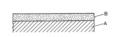
- Figure 1 shows schematically a copper-indium-selenium dispersion layer (B) deposited by dispersion electrolysis on an electrically conductive substrate (A).
- the In and Se contents of the deposition used in this example are readily variable, e.g. in such a way that the Se content is increased and the In content is lowered.
- the sulfamate base instead of the sulfamate base, other bath types are e.g. possible on the basis of chloride, cyanite and sulfate.
Landscapes
- Chemical & Material Sciences (AREA)
- Engineering & Computer Science (AREA)
- Chemical Kinetics & Catalysis (AREA)
- Electrochemistry (AREA)
- Materials Engineering (AREA)
- Metallurgy (AREA)
- Organic Chemistry (AREA)
- Electroplating Methods And Accessories (AREA)
- Photovoltaic Devices (AREA)
- Folding Of Thin Sheet-Like Materials, Special Discharging Devices, And Others (AREA)
- Physical Vapour Deposition (AREA)
Description
- Die Erfindung betrifft ein Verfahren zur Herstellung einer Absorberschicht für Solarzellen, insbesondere einer CuInSe₂-Absorberschicht, mit Hilfe galvanischer Abscheidetechnik, wobei auf einem elektrisch leitenden Substrat eine Halbleiter-Ternärschicht abgeschieden wird, die aus Elementen der ersten und der dritten Nebengruppe sowie der sechsten Hauptgruppe des periodischen Systems der Elemente besteht.
- Eine CuInSe₂-Dünschicht-Solarzelle besteht typischerweise aus einem Substrat, das der Zelle die notwendige Stabilität verleiht. Das Substrat ist mit der erwähnten Absorberschicht beschichtet, die in der Literatur auch als Absorber-Generator bezeichnet wird. Üblicherweise befindet sich zwischen dem Substrat und der Absorberschicht ein großflächiger, metallischer Stromabnahmekontakt. Auf der Oberseite der Absorberschicht befindet sich der Kollektor, mit dessen Hilfe der pn-Übergang erzeugt wird. Beim Beispiel der CuInSe₂-Absorberschicht besteht der Kollektor aus einer Beschichtung aus CdS. Auf der Oberseite des Kollektors ist üblicherweise ein mehr oder weniger feines Gitter aufgebracht, das den Serienwiderstand verringert. Vorstehendes zum allgemeinen Aufbau einer Dünnschicht-Solarzelle wie sie mit Hilfe der nach dem erfindungsgemäßen Verfahren hergestellten Absorberschicht aufgebaut wird.
- Für die Herstellung derartiger Absorberschichten gibt es mehrere aufwendige, meist physikalische Verfahren und unter diesen Verfahren verspricht die Herstellung mit Hilfe galvanischer Abscheidetechnik besonders wirtschaftlich und umweltfreundlich zu sein. Mit dieser Technik befaßt sich daher die vorliegende Erfindung.
- Am erfolgversprechendsten erscheint gegenwärtig eine Solarzelle, deren Absorberschicht aus CuInSe₂ besteht. Die galvanische Herstellung dieser Absorberschicht ist aber bisher gescheitert, zwar konnten aus saurem Cu-Chlorid, In-Chlorid und Se-Oxid-Bädern Schichten der Zusammensetzung CuInSe₂ abgeschieden werden. Solche Ternär-Bäder sind jedoch instabil und kommen daher für eine wirtschaftliche Fertigung nicht in Betracht.
- Zum Stand der Technik wird verwiesen auf
R.N. Bharracharya, Solar Cells, 16 (1986) 237-243,
G. Hodes: Solar Cells, 16 (1986) 245-254,
C.D. Lokhande: I.Electrochem. Soc.,134 (1987) 1727-1729. - Von diesem Stand der Technik geht die Erfindung aus.
- Ihr liegt die Aufgabe zugrunde, ein Verfahren zur Herstellung einer Absorberschicht für Solarzellen mit Hilfe der erfolgversprechenden galvanischen Dispersionsabscheidung vorzuschlagen, die wirtschaftlich durchgeführt werden kann. Insbesondere sollen keine Instabilitäten bei den zum Einsatz kommenden galvanischen Bädern auftreten.
- Die Lösung dieser Aufgabe gelingt gemäß der im Anspruch 1 definierten Erfindung dadurch, daß auf dem Substrat galvanisch eine binäre Legierung aus Ionen der Elemente der ersten und der dritten Nebengruppe des periodensystems abgeschieden wird sowie gleichzeitig der in dem galvanischen Bad suspendierte Legierungsbestandteil der sechsten Hauptgruppe des periodensystems, der durch Dispersionselektrolyse feindispers in die Legierung eingebaut wird.
- Die Erfindung macht sich somit die Erkenntnis zunutze, daß binäre CuIn-Schichten elektrolytisch gut abgeschieden werden können. Der Einbau des Selens - bzw. allgemein des betreffenden Elements der sechten Hauptgruppe des Periodensystems der Elemente - erfolgt erfindungsgemäß durch Dispersionselektrolyse, wodurch die Nachteile beim Stand der Technik vermieden werden, insbesondere geht man nicht mehr den Weg des Abscheidens aus einem Ternärbad, was, wie gesagt, instabil ist.
- Die erfindungsgemäße Verfahrensführung behält die Vorteile der Ein-Schritt-Abscheidung auf galvanischem Wege bei, insbesondere die hohe Materialausnutzung mit großem Durchsatz aufgrund der Möglichkeit einer parallelen Beschichtung mehrerer Substrate bzw. der kontinuierlichen Beschichtung des Substrats. Außerdem können die Absorberschichten ohne nachgeschaltete, umweltbelastende Selenidisierung auf einem beliebigen Metallsubstrat abgeschieden werden.
- Es sei erwähnt, daß Cu und In vorstehend und nachfolgend als Beispiele für die Elemente der ersten und der dritten Nebengruppe des periodensystems der Elemente erwähnt werden und Selen als Beispiel für ein Element der sechsten Hauptgruppe des Periodensystems. Grundsätzlich kommen aber alle anderen Elemente dieser Nebengruppen bzw. der erwähnten Hauptgruppe für das erfindungsgemäße Verfahren infrage.
- Erfindungsgemäß wird somit z.B. eine binäre CuIn-Legierung galvanisch auf einem Metallsubstrat abgeschieden. Gleichzeitig werden aufgrund des Prinzips der Dispersionselektrolyse feine, im Elektrolyt suspendierte Se-Partikel in die sich bildende CuIn-Schicht feindispers eingelagert, so daß nach einer thermisch-chemischen Reaktion der Komponenten als Endprodukt eine ternäre CuInSe₂-Legierung resultiert, d.h. die gewünschte Absorberschicht.
- Ausgestaltungen der Erfindung sind in den Unteransprüchen enthalten.
- Bei Ausführung des Verfahrens in Form einer Bandgalvanisierung bietet sich die kontinuierliche Herstellung von Absorberschichten in technischem Maßstab an. Der Se-Einbau kann sowohl an vertikal als auch an horizontal angeordneten Kathodenwerkstoffen erfolgen. Ein sehr hoher Se-Einbau kann bei horizontaler Kathode durch Ausnutzung des Sedimentationseffekts erreicht werden. Zur Erhöhung des Se-Einbaus in die binäre Legierung können die Se-Partikel auch durch schwere einwertige Metallionen (z.B. Cäsium-Ionen) oder durch oberflächenaktive Substanzen konditioniert werden. Ebenso können zur Erzielung einer optimalen Schichtzusammensetzung bei der Abscheidung die Möglichkeiten der Ultraschallanwendung des Jet-Plating und/oder des Pulse-Plating herangezogen werden.
- Zur Erzeugung einer für die photovoltaische Energieumwandlung optimalen Kristallstruktur und Oberflächenmorphologie kann die beispielhaft angeführte CuInSe₂-Dispersionsschicht einer Diffusions- bzw. Kristallisations-Wärmebehandlung unterzogen werden. Die erfindungsgemäß eingesetzten Se-Pulver können durch Mahlen und Klassieren kommerzieller Pulver auf die erforderliche Feinheit gebracht werden, sie können ebenso durch Reduktion seleniger Säure mit Schwefeldioxid hergestellt und durch Wärmebehandlung in die für Halbleiter erforderliche hexagonal kristallisierte Form gebracht werden.
- Mit dem Verfahren gemäß der Erfindung können somit durch Dispersionselektrolyse auf einfache und umweltschonende Weise Absorberschichten in technischem Maßstab hergestellt werden.
- Weil die Schichtdicke der Absorberschicht üblicherweise einige »m beträgt, muß beispielsweise ein sehr feines Selenpulver verwendet werden. Neben den üblichen Verfahrensmaßnahmen des Mahlens mit anschließendem Klassieren kann dieses auch mit Hilfe der Verfahrensschritte nach Patentanspruch 10 hergestellt werden, wodurch sich ebenfalls ein Pulver mit einer Korngröße in der Größenordnung kleiner als 1»m herstellen läßt.
- Durch die Maßnahmen von Patentanspruch 11 wird das Se-Pulver in die für die Herstellung von Solarzellen besonders vorteilhafte hexagonale Kristallform gebracht.
- Durch die Maßnahmen von Patentanspruch 12 werden die photovoltaischen Eigenschaften der Absorbtionsschicht verbessert.
- Bild 1 zeigt schematisch eine durch Dispersionselektrolyse auf einem elektrisch leitfähigem Substrat (A) abgeschiedene Kupfer-Indium-Selen-Dispersionsschicht (B).
- Im folgenden ist ein Ausführungsbeispiel für das erfindungsgemäße Verfahren aufgeführt.
Aus einem galvanischen Bad auf Sulfamatbasis mit 0,5 mol/l Cu und 0,01 mol/l In, in dem 50 g/l Se-Pulver suspendiert waren, wurde bei einer Stromdichte von 3 A/dm² eine 10 »m dicke, zusammenhängende und auf dem Substrat gut haftende CuInSe-Schicht folgender Zusammensetzung abgeschieden:
Cu = 20,5 Gew.%; In = 44,1 Gew.%; und Se = 35,4 Gew.%. - Die in diesem Beispiel verwendeten In- und Se-Gehalte der Abscheidung sind ohne weiteres variierbar, z.B. in der Weise, daß der Se-Gehalt erhöht und der In-Gehalt erniedrigt wird. Statt der Sulfamatbasis sind auch andere Badtypen z.B. auf der Basis Chlorid, Cyanit und Sulfat möglich.
Claims (12)
- Verfahren zur Herstellung einer Absorberschicht für Solarzellen, insbesondere einer CuInSe₂-Absorberschicht, mit Hilfe galvanischer Abscheidetechnik, wobei auf einem elektrisch leitenden Substrat eine Halbleiter-Ternärschicht abgeschieden wird, die aus Elementen der ersten und der dritten Nebengruppe sowie der sechsten Hauptgruppe des periodischen Systems der Elemente besteht,
dadurch gekennzeichnet,
daß auf dem Substrat galvanisch eine binäre Legierung aus Ionen der Elemente der ersten und der dritten Nebengruppe des Periodensystems abgeschieden und gleichzeitig der in dem galvanischen Bad suspendierte Legierungsbestandteil der sechsten Hauptgruppe des Periodensystems, durch Dispersionselektrolyse feindispers in die Legierung eingebaut wird, die dann durch thermische Nachbehandlung in eine Verbindung des Typs I-III-VI₂ umgewandelt wird. - Verfahren nach Anspruch 1,
dadurch gekennzeichnet,
daß, bezogen auf die binäre Legierung, der Volumenanteil der beiden Komponenten der binären Legierung jeweils zwischen 25 bis 75% beträgt. - Verfahren nach Anspruch 1 oder 2,
dadurch gekennzeichnet,
daß, bezogen auf die Ternärschicht, der Volumenanteil des durch die Dispersionselektrolyse in die binäre Legierung eingebauten Legierungsbestandteile 25 bis 70% beträgt. - Verfahren nach einem der Ansprüche 1 bis 3,
dadurch gekennzeichnet,
daß die Dispersionselektrolyse unter Einsatz von Pulse-Plating, Jet-Plating und/oder Ultraschall erfolgt. - Verfahren nach einem der Ansprüche 1 bis 4,
dadurch gekennzeichnet,
daß die Abscheidung des in dem galvanischen Bad suspendierten Legierungsbestandteils durch Sedimentation unterstützt wird. - Verfahren nach einem der Ansprüche 1 bis 5,
dadurch gekennzeichnet,
daß die Abscheidung nach Art der Bandgalvanisierung kontinuierlich erfolgt. - Verfahren nach einem der Ansprüche 1 bis 6,
dadurch gekennzeichnet,
daß die Konzentration des einzulagernden, im Elektrolyt suspendierten Elements 10 bis 500 g/l beträgt. - Verfahren nach einem der Ansprüche 1 bis 7,
dadurch gekennzeichnet,
daß das einzulagernde Elementpulver mit oberflächenaktiven Substanzen konditioniert wird. - Verfahren nach einem der Ansprüche 1 bis 8,
dadurch gekennzeichnet,
daß das einzulagernde Elementpulver durch Mahlen und Klassieren hergestellt wird. - Verfahren nach einem der Ansprüche 1 bis 8,
dadurch gekennzeichnet,
daß bei Verwendung von Se als einzulagerndes Elementpulver dieses durch Reduktion von seleniger Säure mit Schwefeldioxid hergestellt wird. - Verfahren nach einem der Ansprüche 1 bis 10,
dadurch gekennzeichnet,
daß bei Verwendung von Se als einzulagerndes Elementpulver dieses durch eine Wärmebehandlung in eine halbleitende hexagonale Kristallform gebracht worden ist. - Verfahren nach einem der Ansprüche 1 bis 11,
dadurch gekennzeichnet,
daß die Beschichtung des Substrats einer Diffusionserwärmung unterworfen wird.
Applications Claiming Priority (5)
| Application Number | Priority Date | Filing Date | Title |
|---|---|---|---|
| DE4030057 | 1990-09-22 | ||
| DE4030057 | 1990-09-22 | ||
| DE4103291A DE4103291A1 (de) | 1990-09-22 | 1991-02-04 | Verfahren zur herstellung einer absorberschicht fuer solarzellen mit hilfe galvanischer abscheidetechnik |
| DE4103291 | 1991-02-04 | ||
| PCT/EP1991/001708 WO1992005586A1 (de) | 1990-09-22 | 1991-09-09 | Verfahren zur herstellung einer absorberschicht für solarzellen mit hilfe galvanischer abscheidetechnik |
Publications (2)
| Publication Number | Publication Date |
|---|---|
| EP0502148A1 EP0502148A1 (de) | 1992-09-09 |
| EP0502148B1 true EP0502148B1 (de) | 1995-05-24 |
Family
ID=25897096
Family Applications (1)
| Application Number | Title | Priority Date | Filing Date |
|---|---|---|---|
| EP91915927A Expired - Lifetime EP0502148B1 (de) | 1990-09-22 | 1991-09-09 | Verfahren zur herstellung einer absorberschicht für solarzellen mit hilfe galvanischer abscheidetechnik |
Country Status (7)
| Country | Link |
|---|---|
| US (1) | US5275714A (de) |
| EP (1) | EP0502148B1 (de) |
| JP (1) | JP2756187B2 (de) |
| AT (1) | ATE123177T1 (de) |
| DE (2) | DE4103291A1 (de) |
| ES (1) | ES2075461T3 (de) |
| WO (1) | WO1992005586A1 (de) |
Families Citing this family (29)
| Publication number | Priority date | Publication date | Assignee | Title |
|---|---|---|---|---|
| JPH0788063A (ja) * | 1991-05-08 | 1995-04-04 | Sharp Corp | ハンドル取付構造 |
| DE4217454B4 (de) * | 1991-05-27 | 2004-09-30 | Fuji Electric Corporate Research & Development Ltd., Yokosuka | CuInSe-2-Dünnschicht-Solarzelle und Verfahren zu ihrer Herstellung |
| CH687112A5 (fr) * | 1993-06-08 | 1996-09-13 | Yazaki Corp | Procédé pour déposer un précurseur du composé CuInSe(2). |
| JP2806469B2 (ja) * | 1993-09-16 | 1998-09-30 | 矢崎総業株式会社 | 太陽電池吸収層の製造方法 |
| JP2967908B2 (ja) * | 1994-09-21 | 1999-10-25 | 矢崎総業株式会社 | 分散めっき法と太陽電池の製造方法 |
| US5772431A (en) * | 1995-05-22 | 1998-06-30 | Yazaki Corporation | Thin-film solar cell manufacturing apparatus and manufacturing method |
| JP3089994B2 (ja) * | 1995-07-26 | 2000-09-18 | 矢崎総業株式会社 | 銅−インジウム−硫黄−セレン薄膜の作製方法、及び銅−インジウム−硫黄−セレン系カルコパイライト結晶の製造方法 |
| US5712187A (en) * | 1995-11-09 | 1998-01-27 | Midwest Research Institute | Variable temperature semiconductor film deposition |
| DE19634580C2 (de) * | 1996-08-27 | 1998-07-02 | Inst Solar Technologien | Verfahren zur Herstellung einer CIS-Bandsolarzelle und Vorrichtung zur Durchführung des Verfahrens |
| US6268014B1 (en) | 1997-10-02 | 2001-07-31 | Chris Eberspacher | Method for forming solar cell materials from particulars |
| US6379521B1 (en) * | 1998-01-06 | 2002-04-30 | Canon Kabushiki Kaisha | Method of producing zinc oxide film, method of producing photovoltaic element, and method of producing semiconductor element substrate |
| DE19917758C2 (de) * | 1999-04-10 | 2003-08-28 | Cis Solartechnik Gmbh | Verfahren zur Herstellung einer CuInSe2(CIS)Solarzelle |
| US6159853A (en) * | 1999-08-04 | 2000-12-12 | Industrial Technology Research Institute | Method for using ultrasound for assisting forming conductive layers on semiconductor devices |
| GB2386907B (en) * | 2002-03-27 | 2005-10-26 | Isle Coat Ltd | Process and device for forming ceramic coatings on metals and alloys, and coatings produced by this process |
| FR2849532B1 (fr) * | 2002-12-26 | 2005-08-19 | Electricite De France | Procede de fabrication d'un compose i-iii-vi2 en couches minces, favorisant l'incorporation d'elements iii |
| TW200425940A (en) * | 2003-05-16 | 2004-12-01 | Chung Shan Inst Of Science | An air cleaning florescent lamp coated with photocatalysis materials |
| US8309163B2 (en) * | 2004-02-19 | 2012-11-13 | Nanosolar, Inc. | High-throughput printing of semiconductor precursor layer by use of chalcogen-containing vapor and inter-metallic material |
| US7306823B2 (en) * | 2004-09-18 | 2007-12-11 | Nanosolar, Inc. | Coated nanoparticles and quantum dots for solution-based fabrication of photovoltaic cells |
| US8623448B2 (en) * | 2004-02-19 | 2014-01-07 | Nanosolar, Inc. | High-throughput printing of semiconductor precursor layer from chalcogenide microflake particles |
| US8329501B1 (en) | 2004-02-19 | 2012-12-11 | Nanosolar, Inc. | High-throughput printing of semiconductor precursor layer from inter-metallic microflake particles |
| US8372734B2 (en) | 2004-02-19 | 2013-02-12 | Nanosolar, Inc | High-throughput printing of semiconductor precursor layer from chalcogenide nanoflake particles |
| KR100850000B1 (ko) * | 2005-09-06 | 2008-08-01 | 주식회사 엘지화학 | 태양전지 흡수층의 제조방법 |
| US20070227633A1 (en) * | 2006-04-04 | 2007-10-04 | Basol Bulent M | Composition control for roll-to-roll processed photovoltaic films |
| US7736913B2 (en) * | 2006-04-04 | 2010-06-15 | Solopower, Inc. | Composition control for photovoltaic thin film manufacturing |
| US7892413B2 (en) * | 2006-09-27 | 2011-02-22 | Solopower, Inc. | Electroplating methods and chemistries for deposition of copper-indium-gallium containing thin films |
| US8425753B2 (en) * | 2008-05-19 | 2013-04-23 | Solopower, Inc. | Electroplating methods and chemistries for deposition of copper-indium-gallium containing thin films |
| US20100213073A1 (en) * | 2009-02-23 | 2010-08-26 | International Business Machines Corporation | Bath for electroplating a i-iii-vi compound, use thereof and structures containing same |
| US8618411B2 (en) * | 2009-04-08 | 2013-12-31 | David M. Schwartz | Method of making photovoltaic cell |
| FR2957365B1 (fr) * | 2010-03-11 | 2012-04-27 | Electricite De France | Procede de preparation d'une couche mince d'absorbeur pour cellules photovoltaiques |
Family Cites Families (6)
| Publication number | Priority date | Publication date | Assignee | Title |
|---|---|---|---|---|
| JPS61237476A (ja) * | 1985-04-12 | 1986-10-22 | シーメンス・ソラー・インダストリエス・リミテッド・パートナーシップ | 化合物半導体の製造方法 |
| US4612411A (en) * | 1985-06-04 | 1986-09-16 | Atlantic Richfield Company | Thin film solar cell with ZnO window layer |
| GB8715082D0 (en) * | 1987-06-26 | 1987-08-05 | Prutec Ltd | Solar cells |
| DE3887650T2 (de) * | 1987-11-27 | 1994-08-04 | Siemens Solar Ind Lp | Herstellungsverfahren einer Dünnschichtsonnenzelle. |
| DE3822073A1 (de) * | 1988-06-30 | 1990-01-04 | Bloss Werner Heinz Prof Dr Ing | Verfahren zur herstellung von verbindungshalbleiter-duennschichten |
| US4915745A (en) * | 1988-09-22 | 1990-04-10 | Atlantic Richfield Company | Thin film solar cell and method of making |
-
1991
- 1991-02-04 DE DE4103291A patent/DE4103291A1/de active Granted
- 1991-09-09 US US07/852,200 patent/US5275714A/en not_active Expired - Lifetime
- 1991-09-09 JP JP3514716A patent/JP2756187B2/ja not_active Expired - Fee Related
- 1991-09-09 AT AT91915927T patent/ATE123177T1/de active
- 1991-09-09 ES ES91915927T patent/ES2075461T3/es not_active Expired - Lifetime
- 1991-09-09 DE DE59105590T patent/DE59105590D1/de not_active Expired - Lifetime
- 1991-09-09 EP EP91915927A patent/EP0502148B1/de not_active Expired - Lifetime
- 1991-09-09 WO PCT/EP1991/001708 patent/WO1992005586A1/de not_active Ceased
Also Published As
| Publication number | Publication date |
|---|---|
| ATE123177T1 (de) | 1995-06-15 |
| EP0502148A1 (de) | 1992-09-09 |
| JPH05506334A (ja) | 1993-09-16 |
| DE4103291C2 (de) | 1992-09-17 |
| DE59105590D1 (de) | 1995-06-29 |
| WO1992005586A1 (de) | 1992-04-02 |
| DE4103291A1 (de) | 1992-04-02 |
| JP2756187B2 (ja) | 1998-05-25 |
| ES2075461T3 (es) | 1995-10-01 |
| US5275714A (en) | 1994-01-04 |
Similar Documents
| Publication | Publication Date | Title |
|---|---|---|
| DE4103291C2 (de) | ||
| DE69621467T2 (de) | Vorbereitung von cu x in y ga z se n (x=0-2, y = 0-2, z = 0-2, n = 0-3) vorläuferfilmen durch elektroplattierung zur herstellung von solarzellen von hohem wirkungsgrad | |
| DE112011102300B4 (de) | Verfahren zum ausbilden einer p-halbleiterschicht für eine photovoltaikeinheit | |
| DE4433097A1 (de) | Verfahren zum Herstellen einer lichtabsorbierenden Schicht einer Solarzelle | |
| EP0922303B1 (de) | Cis-bandsolarzelle-verfahren und vorrichtung zu ihrer herstellung | |
| Pottier et al. | Preparation of polycrystalline thin films of CuInSe2 by electrodeposition | |
| DE69434829T2 (de) | HERSTELLUNGSVERFAHREN FÜR EINE CuInSe2-VERBINDUNG | |
| DE19630321C2 (de) | Verfahren zur Herstellung eines Kupfer-Indium-Schwefel-Selen-Dünnfilms und zur Herstellung eines Kupfer-Indium-Schwefel-Selen-Chalcopyrit-Kristalls | |
| DE3887650T2 (de) | Herstellungsverfahren einer Dünnschichtsonnenzelle. | |
| DE3686605T2 (de) | Photovoltaische duennfilmvorrichtung. | |
| DE3307748A1 (de) | Verfahren zum behandeln einer metallfolie zwecks verbesserung ihres haftvermoegens | |
| DE19921515A1 (de) | Dünnschichtsolarzelle auf der Basis der Ia/IIIb/VIa- Verbindungshalbleiter und Verfahren zu ihrer Herstellung | |
| DE10113782A1 (de) | Solarzelle und Verfahren zu ihrer Herstellung | |
| Chraibi et al. | Influence of citrate ions as complexing agent for electrodeposition of CuInSe2 thin films | |
| EP1792348A1 (de) | Verfahren zum aufbringen einer zinksulfid-pufferschicht auf ein halbleitersubstrat mittels chemischer badabscheidung, insbesondere auf die absorberschicht einer chalkopyrit-dünnschicht-solarzelle | |
| US20130112564A1 (en) | Electroplating Solutions and Methods For Deposition of Group IIIA-VIA Films | |
| DE2726009A1 (de) | Verfahren und vorrichtung zum erzeugen von lichtelektrischer energie | |
| DE102012216026A1 (de) | Verfahren zur Herstellung einer flexiblen Photovoltaik-Dünnschichtzelle mit einer Eisendiffusionsbarriereschicht | |
| US20100200050A1 (en) | Electroplating methods and chemistries for deposition of copper-indium-gallium containing thin films | |
| Herrero et al. | Electrodeposition of Cu In alloys for preparing CuInS2 thin films | |
| DE3586847T2 (de) | Herstellungsverfahren eines zusammengesetzten halbleiters. | |
| DE2337899B2 (de) | Verfahren zur Herstellung einer negativen Kadmiumelektrode für galvanische Elemente | |
| EP2411558B1 (de) | VERFAHREN ZUM AUFBRINGEN EINER Zn(S, O)-PUFFERSCHICHT AUF EIN HALBLEITERSUBSTRAT MITTELS CHEMISCHER BADABSCHEIDUNG | |
| Jeyakumar et al. | Electrochemical preparation and characterization of copper indium diselenide thin films | |
| EP4010515A1 (de) | Verfahren und anlage zum elektrolytischen beschichten eines elektrisch leitfähigen bandes und/oder gewebes mittels pulstechnik |
Legal Events
| Date | Code | Title | Description |
|---|---|---|---|
| PUAI | Public reference made under article 153(3) epc to a published international application that has entered the european phase |
Free format text: ORIGINAL CODE: 0009012 |
|
| 17P | Request for examination filed |
Effective date: 19920511 |
|
| AK | Designated contracting states |
Kind code of ref document: A1 Designated state(s): AT BE CH DE DK ES FR GB GR IT LI LU NL SE |
|
| RAP1 | Party data changed (applicant data changed or rights of an application transferred) |
Owner name: BATTELLE MEMORIAL INSTITUTE |
|
| 17Q | First examination report despatched |
Effective date: 19940711 |
|
| GRAA | (expected) grant |
Free format text: ORIGINAL CODE: 0009210 |
|
| AK | Designated contracting states |
Kind code of ref document: B1 Designated state(s): AT BE CH DE DK ES FR GB GR IT LI LU NL SE |
|
| PG25 | Lapsed in a contracting state [announced via postgrant information from national office to epo] |
Ref country code: NL Free format text: LAPSE BECAUSE OF NON-PAYMENT OF DUE FEES Effective date: 19950524 Ref country code: DK Effective date: 19950524 Ref country code: BE Effective date: 19950524 Ref country code: GR Free format text: LAPSE BECAUSE OF FAILURE TO SUBMIT A TRANSLATION OF THE DESCRIPTION OR TO PAY THE FEE WITHIN THE PRESCRIBED TIME-LIMIT Effective date: 19950524 |
|
| REF | Corresponds to: |
Ref document number: 123177 Country of ref document: AT Date of ref document: 19950615 Kind code of ref document: T |
|
| REF | Corresponds to: |
Ref document number: 59105590 Country of ref document: DE Date of ref document: 19950629 |
|
| REG | Reference to a national code |
Ref country code: CH Ref legal event code: PUE Owner name: YAZAKI CORPORATION |
|
| RAP2 | Party data changed (patent owner data changed or rights of a patent transferred) |
Owner name: YAZAKI CORPORATION |
|
| ITF | It: translation for a ep patent filed | ||
| PG25 | Lapsed in a contracting state [announced via postgrant information from national office to epo] |
Ref country code: SE Effective date: 19950824 |
|
| PG25 | Lapsed in a contracting state [announced via postgrant information from national office to epo] |
Ref country code: AT Effective date: 19950909 |
|
| ET | Fr: translation filed | ||
| GBT | Gb: translation of ep patent filed (gb section 77(6)(a)/1977) |
Effective date: 19950822 |
|
| PG25 | Lapsed in a contracting state [announced via postgrant information from national office to epo] |
Ref country code: LU Free format text: LAPSE BECAUSE OF NON-PAYMENT OF DUE FEES Effective date: 19950930 |
|
| REG | Reference to a national code |
Ref country code: ES Ref legal event code: FG2A Ref document number: 2075461 Country of ref document: ES Kind code of ref document: T3 |
|
| NLT2 | Nl: modifications (of names), taken from the european patent patent bulletin |
Owner name: YAZAKI CORPORATION |
|
| NLV1 | Nl: lapsed or annulled due to failure to fulfill the requirements of art. 29p and 29m of the patents act | ||
| PLBE | No opposition filed within time limit |
Free format text: ORIGINAL CODE: 0009261 |
|
| STAA | Information on the status of an ep patent application or granted ep patent |
Free format text: STATUS: NO OPPOSITION FILED WITHIN TIME LIMIT |
|
| 26N | No opposition filed | ||
| REG | Reference to a national code |
Ref country code: CH Ref legal event code: NV Representative=s name: MOINAS KIEHL SAVOYE & CRONIN |
|
| REG | Reference to a national code |
Ref country code: GB Ref legal event code: IF02 |
|
| PGFP | Annual fee paid to national office [announced via postgrant information from national office to epo] |
Ref country code: GB Payment date: 20060906 Year of fee payment: 16 |
|
| PGFP | Annual fee paid to national office [announced via postgrant information from national office to epo] |
Ref country code: FR Payment date: 20060908 Year of fee payment: 16 |
|
| PGFP | Annual fee paid to national office [announced via postgrant information from national office to epo] |
Ref country code: CH Payment date: 20060913 Year of fee payment: 16 |
|
| PGFP | Annual fee paid to national office [announced via postgrant information from national office to epo] |
Ref country code: IT Payment date: 20060930 Year of fee payment: 16 |
|
| PGFP | Annual fee paid to national office [announced via postgrant information from national office to epo] |
Ref country code: ES Payment date: 20061003 Year of fee payment: 16 |
|
| REG | Reference to a national code |
Ref country code: CH Ref legal event code: PL |
|
| GBPC | Gb: european patent ceased through non-payment of renewal fee |
Effective date: 20070909 |
|
| PG25 | Lapsed in a contracting state [announced via postgrant information from national office to epo] |
Ref country code: LI Free format text: LAPSE BECAUSE OF NON-PAYMENT OF DUE FEES Effective date: 20070930 Ref country code: CH Free format text: LAPSE BECAUSE OF NON-PAYMENT OF DUE FEES Effective date: 20070930 |
|
| REG | Reference to a national code |
Ref country code: FR Ref legal event code: ST Effective date: 20080531 |
|
| PG25 | Lapsed in a contracting state [announced via postgrant information from national office to epo] |
Ref country code: FR Free format text: LAPSE BECAUSE OF NON-PAYMENT OF DUE FEES Effective date: 20071001 |
|
| PG25 | Lapsed in a contracting state [announced via postgrant information from national office to epo] |
Ref country code: GB Free format text: LAPSE BECAUSE OF NON-PAYMENT OF DUE FEES Effective date: 20070909 |
|
| REG | Reference to a national code |
Ref country code: ES Ref legal event code: FD2A Effective date: 20070910 |
|
| PG25 | Lapsed in a contracting state [announced via postgrant information from national office to epo] |
Ref country code: ES Free format text: LAPSE BECAUSE OF NON-PAYMENT OF DUE FEES Effective date: 20070910 |
|
| PG25 | Lapsed in a contracting state [announced via postgrant information from national office to epo] |
Ref country code: IT Free format text: LAPSE BECAUSE OF NON-PAYMENT OF DUE FEES Effective date: 20070909 |
|
| PGFP | Annual fee paid to national office [announced via postgrant information from national office to epo] |
Ref country code: DE Payment date: 20100901 Year of fee payment: 20 |
|
| REG | Reference to a national code |
Ref country code: DE Ref legal event code: R071 Ref document number: 59105590 Country of ref document: DE |
|
| REG | Reference to a national code |
Ref country code: DE Ref legal event code: R071 Ref document number: 59105590 Country of ref document: DE |
|
| PG25 | Lapsed in a contracting state [announced via postgrant information from national office to epo] |
Ref country code: DE Free format text: LAPSE BECAUSE OF EXPIRATION OF PROTECTION Effective date: 20110910 |