EP0485187A2 - Vorrichtung zur Erzeugung der zweiten Harmonischen einer von einer Laserquelle erzeugten Grundschwingung - Google Patents
Vorrichtung zur Erzeugung der zweiten Harmonischen einer von einer Laserquelle erzeugten Grundschwingung Download PDFInfo
- Publication number
- EP0485187A2 EP0485187A2 EP91310248A EP91310248A EP0485187A2 EP 0485187 A2 EP0485187 A2 EP 0485187A2 EP 91310248 A EP91310248 A EP 91310248A EP 91310248 A EP91310248 A EP 91310248A EP 0485187 A2 EP0485187 A2 EP 0485187A2
- Authority
- EP
- European Patent Office
- Prior art keywords
- light
- quasi
- phase matching
- semiconductor laser
- harmonic
- Prior art date
- Legal status (The legal status is an assumption and is not a legal conclusion. Google has not performed a legal analysis and makes no representation as to the accuracy of the status listed.)
- Granted
Links
Images


Classifications
-
- H—ELECTRICITY
- H01—ELECTRIC ELEMENTS
- H01S—DEVICES USING THE PROCESS OF LIGHT AMPLIFICATION BY STIMULATED EMISSION OF RADIATION [LASER] TO AMPLIFY OR GENERATE LIGHT; DEVICES USING STIMULATED EMISSION OF ELECTROMAGNETIC RADIATION IN WAVE RANGES OTHER THAN OPTICAL
- H01S5/00—Semiconductor lasers
- H01S5/10—Construction or shape of the optical resonator, e.g. extended or external cavity, coupled cavities, bent-guide, varying width, thickness or composition of the active region
- H01S5/14—External cavity lasers
-
- G—PHYSICS
- G02—OPTICS
- G02F—OPTICAL DEVICES OR ARRANGEMENTS FOR THE CONTROL OF LIGHT BY MODIFICATION OF THE OPTICAL PROPERTIES OF THE MEDIA OF THE ELEMENTS INVOLVED THEREIN; NON-LINEAR OPTICS; FREQUENCY-CHANGING OF LIGHT; OPTICAL LOGIC ELEMENTS; OPTICAL ANALOGUE/DIGITAL CONVERTERS
- G02F1/00—Devices or arrangements for the control of the intensity, colour, phase, polarisation or direction of light arriving from an independent light source, e.g. switching, gating or modulating; Non-linear optics
- G02F1/35—Non-linear optics
- G02F1/37—Non-linear optics for second-harmonic generation
- G02F1/377—Non-linear optics for second-harmonic generation in an optical waveguide structure
- G02F1/3775—Non-linear optics for second-harmonic generation in an optical waveguide structure with a periodic structure, e.g. domain inversion, for quasi-phase-matching [QPM]
-
- G—PHYSICS
- G02—OPTICS
- G02F—OPTICAL DEVICES OR ARRANGEMENTS FOR THE CONTROL OF LIGHT BY MODIFICATION OF THE OPTICAL PROPERTIES OF THE MEDIA OF THE ELEMENTS INVOLVED THEREIN; NON-LINEAR OPTICS; FREQUENCY-CHANGING OF LIGHT; OPTICAL LOGIC ELEMENTS; OPTICAL ANALOGUE/DIGITAL CONVERTERS
- G02F1/00—Devices or arrangements for the control of the intensity, colour, phase, polarisation or direction of light arriving from an independent light source, e.g. switching, gating or modulating; Non-linear optics
- G02F1/35—Non-linear optics
- G02F1/37—Non-linear optics for second-harmonic generation
- G02F1/377—Non-linear optics for second-harmonic generation in an optical waveguide structure
- G02F1/383—Non-linear optics for second-harmonic generation in an optical waveguide structure of the optical fibre type
-
- H—ELECTRICITY
- H01—ELECTRIC ELEMENTS
- H01S—DEVICES USING THE PROCESS OF LIGHT AMPLIFICATION BY STIMULATED EMISSION OF RADIATION [LASER] TO AMPLIFY OR GENERATE LIGHT; DEVICES USING STIMULATED EMISSION OF ELECTROMAGNETIC RADIATION IN WAVE RANGES OTHER THAN OPTICAL
- H01S3/00—Lasers, i.e. devices using stimulated emission of electromagnetic radiation in the infrared, visible or ultraviolet wave range
- H01S3/10—Controlling the intensity, frequency, phase, polarisation or direction of the emitted radiation, e.g. switching, gating, modulating or demodulating
- H01S3/106—Controlling the intensity, frequency, phase, polarisation or direction of the emitted radiation, e.g. switching, gating, modulating or demodulating by controlling devices placed within the cavity
- H01S3/108—Controlling the intensity, frequency, phase, polarisation or direction of the emitted radiation, e.g. switching, gating, modulating or demodulating by controlling devices placed within the cavity using non-linear optical devices, e.g. exhibiting Brillouin or Raman scattering
- H01S3/109—Frequency multiplication, e.g. harmonic generation
-
- H—ELECTRICITY
- H01—ELECTRIC ELEMENTS
- H01S—DEVICES USING THE PROCESS OF LIGHT AMPLIFICATION BY STIMULATED EMISSION OF RADIATION [LASER] TO AMPLIFY OR GENERATE LIGHT; DEVICES USING STIMULATED EMISSION OF ELECTROMAGNETIC RADIATION IN WAVE RANGES OTHER THAN OPTICAL
- H01S5/00—Semiconductor lasers
- H01S5/005—Optical components external to the laser cavity, specially adapted therefor, e.g. for homogenisation or merging of the beams or for manipulating laser pulses, e.g. pulse shaping
- H01S5/0092—Optical components external to the laser cavity, specially adapted therefor, e.g. for homogenisation or merging of the beams or for manipulating laser pulses, e.g. pulse shaping for nonlinear frequency conversion, e.g. second harmonic generation [SHG] or sum- or difference-frequency generation outside the laser cavity
-
- H—ELECTRICITY
- H01—ELECTRIC ELEMENTS
- H01S—DEVICES USING THE PROCESS OF LIGHT AMPLIFICATION BY STIMULATED EMISSION OF RADIATION [LASER] TO AMPLIFY OR GENERATE LIGHT; DEVICES USING STIMULATED EMISSION OF ELECTROMAGNETIC RADIATION IN WAVE RANGES OTHER THAN OPTICAL
- H01S5/00—Semiconductor lasers
- H01S5/02—Structural details or components not essential to laser action
- H01S5/028—Coatings ; Treatment of the laser facets, e.g. etching, passivation layers or reflecting layers
Definitions
- the present invention relates to a second harmonic generator using a laser as a fundamental wave light source.
- This type of second harmonic generator is adapted to reduce the wavelength of an output light from a light source into half for the purpose of reduction of the wavelength.
- Second harmonic generating elements also termed as SHG elements
- SHG elements used in such a device are disclosed in E.J. Lim, et al, "Blue Light Generation by Frequency Doubling in Periodically Polled Lithium Niobate Channel Waveguide” Electronics Letters, Vol. 25, No. 11, pp. 731-732 (1989).
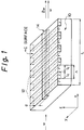
- FIG. 1 is a schematic perspective view of a second harmonic generating element, a concept of principle of operation, or quasi-phase matching method, of the SHG element, will be described.
- a LiNbO3 substrate 10 has a +C surface in which Ti (titanium) has been thermally diffused periodically with the period of ⁇ at the diffusion temperature of about 1,100°C for the diffusion time of about one hour to form a domain inversion structure 12, which is a grating-like structure.
- An optical waveguide 14 is formed by a proton exchange method (Li+ - H+ exchange method) perpendicular to the domain inversion structure 12.
- m 0, 1, 2, ...
- Nn effective guide index of refractive index
- coherence length lc depends on the fundamental wavelength ⁇ ( ⁇ ) and the size of the optical waveguide.
- the amount lc is said to be on the order of 1.7 micron or micrometer ( ⁇ m)
- Coherence length lc being 1.7 micron means that the intensity of the second harmonic becomes maximal as the fundamental wave propagates in the optical waveguide 14 by a length of 1.7 micron, and then becomes 0 (zero) as it propagates by a further length of 1.7 micron.
- coherence length lc is finite rather than infinite indicates that phase matching between the fundamental wave and the second harmonic is incomplete, and that if the fundamental wave propagates in the optical waveguide 14 over a distance longer than the coherence length lc, the intensity of the second harmonic will not exceed a certain value.
- phase mismatching ⁇ k (4 ⁇ / ⁇ ( ⁇ ))(N(2 ⁇ )) - N( ⁇ )).
- the use of a dye laser for the light source for fundamental wave leads to increased size of the overall second harmonic generator, and the second harmonic generator using a dye laser for the light source for fundamental wave is of substantially no practical use because a monochromatic laser light is already available by gas laser or the like.
- a practically useful second harmonic generator can be constructed using a semiconductor laser (hereafter, abbreviated as LD) more compact than the dye laser for the fundamental wave light source and adopting a technology making an oscillation wavelength variable.
- LD semiconductor laser
- a second harmonic generator which is compact, uses a semiconductor laser for a fundamental wave light source and a second harmonic generating element based on a quasi-phase matching method and can produce a high power, short wavelength laser beam.
- a second harmonic generator comprises a semiconductor laser chip having an active layer therein acting as a semiconductor laser for a fundamental wave light source for emitting a laser light, and a quasi-phase matching element optically coupled to the semiconductor laser chip to allow said semiconductor laser chip to lase utilizing feedback of a light from said quasi-phase matching element, the quasi-phase matching element being adapted to generate a second harmonic light using the laser light emitted from said semiconductor laser chip as a fundamental wave light.
- the quasi-phase matching element may preferably comprise an optical waveguide having a periodical guide index distribution structure.
- the semiconductor laser chip may preferably have a first chip end and a second chip end each of which is capable of emitting a light, in which the second chip end of the semiconductor laser chip is an end on which the semiconductor laser chip is optically coupled with the quasi-phase matching element, and the first chip end of the semiconductor laser chip and the periodical guide index distribution structure of the quasi-phase matching element may constitute an external optical resonator for lasing the semiconductor laser chip.
- the second harmonic generator may further comprise a structure for lasing of the semiconductor laser chip utilizing feedback of a light from the periodical guide index distribution structure.
- the semiconductor chip and the quasi-phase matching element may preferably be arranged so that the feedback of the light from the optical waveguide in the quasi-phase matching element is made into the active layer in the semiconductor laser chip.
- the semiconductor laser chip may preferably have a first chip end and a second chip end each of which is capable of emitting a light, in which the second chip end of the semiconductor laser chip is an end on which the semiconductor laser chip is optically coupled with the quasi-phase matching element, in which the first chip end of the semiconductor laser chip has provided thereon a first (higher) reflection coating film constituting an external optical resonator for lasing of the semiconductor laser chip; and in which the second chip end of the semiconductor laser chip has provided thereon a second (lower) reflection coating film free of contribution to the lasing of the semiconductor laser chip.
- the periodical guide index distribution structure may preferably have a reflection effect on the fundamental wave light.
- periodical guide index distribution structure may preferably have a transmission effect on the second harmonic light.
- the periodical guide index distribution structure may preferably have a period of variation of a guide index satisfying:
- the quasi-phase matching element may preferably comprise a LiNbO3 substrate having a +C surface, an optical waveguide formed on the +C surface of the substrate by a Li+ - H+ proton exchange method, and a periodical guide index distribution structure formed in the optical waveguide by Ti diffusion.
- the quasi-phase matching element may preferably have a first element end capable of introduction and emission of the fundamental wave light, and a second element end capable of introduction and emission of the second harmonic light.
- each of the first and second element ends may have a second reflection coating film to keep reflection of the fundamental wave light and the second harmonic light to respective predetermined (low) levels.
- the second harmonic generator may preferably have a 1/2 wavelength plate inserted between the semiconductor laser chip and the quasi-phase matching element.
- the active layer of the semiconductor layer chip and the optical waveguide of the quasi-phase matching element may preferably be optically coupled with each other.
- the quasi-phase matching element may be of a planar type or of an optical fiber type.
- the semiconductor laser chip may preferably be adapted to be used under application of an operation current in a range free of lasing with the semiconductor laser chip alone.
- the quasi-phase matching element may preferably comprise a crystal substrate having a +C face as a surface, in which the quasi-phase matching element has a first element end on a side of the semiconductor laser chip, the first element end being capable of introduction and emission of the fundamental wave light, and a second element end opposite to the first element end capable of introduction and emission of the second harmonic light, in which the optical waveguide extends between the first and second element ends, the first and second element ends being inclined at interior angles ⁇ 1 and ⁇ 2, respectively, with respect to the +C face, and in which the semiconductor laser chip and the quasi-phase matching element are arranged so that the fundamental wave light can be incident into the optical waveguide at Brewster angle or an angle approximate thereto.
- the crystal substrate may include a substrate layer in which material of the crystal substrate remains unchanged, in which the optical waveguide and the substrate layer define therebetween an interface, the interface being parallel to the +C face; and in which the interior angle ⁇ 1 is set up at a value at which the fundamental wave light and the second harmonic light in the optical waveguide can enter the interface and the +C face at a total reflection angle.
- the interior angle ⁇ 1 may satisfy an expresion of 49.2° ⁇ ⁇ 1 ⁇ 83.3°, when the fundamental wave light has a wavelength of 830 nm.
- the first and second element ends and the +C face may preferably define respective edges parallel to each other.
- the crystal substrate may include a substrate layer in which material of the crystal substrate remains unchanged, in which the optical waveguide and the substrate layer define therebetween an interface, the interface being parallel to the +C face, and in which the interior angle ⁇ 1 is set up at a value at which the fundamental wave light and the second harmonic light in the optical waveguide can enter the interface and the +C face at a total reflection angle.
- a semiconductor laser is used instead of a dye laser which has been used conventionally, and a laser beam from the semiconductor laser is launched into a quasi-phase matching element as a light of a fundamental wave, resulting in that a second harmonic of the fundamental wave is emitted from the quasi-phase matching element. Therefore, the whole structure of the second harmonic generator is compacter and smaller than the conventional one using a dye laser.
- the quasi-phase matching element includes a substrate and an optical waveguide formed on the surface thereof.
- the optical waveguide is formed periodically a domain inversion region.
- the domain inversion regions thus formed have each a refractive index slightly higher than the remaining part of the optical waveguide. This construction may be deemed as forming a diffraction grating along the direction of optical guiding when the optical waveguide is viewed as a whole. Therefore, the domain inversion regions form a periodical guide index distribution structure.
- the periodical guide index distribution structure is constructed such that the period of guide index variation, i.e., period of formation of domain inversion regions satisfies the following three conditions:
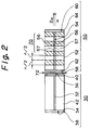
- FIG. 2 is a schematic cross sectional view of a second harmonic generator according to one embodiment of the present invention.
- the second harmonic generator is an apparatus utilizing a semiconductor laser for a fundamental wave light source, and hence the second harmonic generator of the present invention includes a semiconductor chip (hereafter, sometimes referred to simply as LD chip) 30 and a quasi-phase matching element (hereafter, sometimes referred to simply as SHG element) 50 optically connected to one another.
- This construction permits the quasi-phase matching element 50 to generate and emit a light of second harmonic using a laser beam emitted from the semiconductor laser chip 30 as a fundamental wave light.
- the semiconductor laser chip 30 includes an active layer 32 which emits a light and serves as an optical waveguide and both radiation ends of the active layer 32 are substantially perpendicular to the direction in which light is guided, and these ends are termed as a first chip end 34 and a second chip end 36.
- a peripheral semiconductor region around the active layer 32 is indicated by 42.
- the semiconductor chip has a coating film formed at the radiation ends thereof so that the radiation ends on which the laser beam is reflected can establish a predetermined reflectivity (for example, about 30 %).
- a predetermined reflectivity for example, about 30 %.
- the semiconductor chip can lase alone without being combined with any quasi-phase matching element unlike the instant embodiment of the present invention.
- ordinary semiconductor chips used alone for lasing have respective oscillation wavelengths fixed to ones specific to the chips.
- the semiconductor laser chip 30 is adapted to lase at a wavelength of a fundamental wave light satisfying quasi-phase matching conditions of the quasi-phase matching element 50. Therefore, a usually employed laser chip lasing alone cannot be used for the laser chip 30 in the present invention.
- the semiconductor laser chip 30 included in the present invention is used in an operation current range in which no lasing will occur by itself although light emission occurs in the active layer 32.
- a high reflection coating film (hereafter, sometimes referred to simply as HR coating film) 38 contributing to lasing be provided on the first chip end 34 while on the second chip end 36 be provided a low reflection coating film (hereafter, sometimes referred to simply as AR coating film) 40 which does not contribute to lasing to obtain a construction which will not permit the oscillation of LD chip 30 by itself.
- HR coating film high reflection coating film
- AR coating film low reflection coating film
- the HR and AR coating films 38 and 40 mean that they are highly and lowly reflective, respectively, for both wavelengths of the laser light (fundamental wave light, also referred to simply as fundamental wave or fundamental light) and of the second harmonic (also referred to as SH light) which will be discussed later on.
- the reflectivity of the HR coating film 38 is desirably 10% in ideal cases but it is suitable that it is as close thereto as possible.
- the reflectivity of the AR coating film 40 is desirably 0 %. It is also suitable that it is as close thereto as possible.
- the quasi-phase matching element 50 used in the present invention may basically be of the same construction as the conventional planar type quasi-phase matching element described above. In the instant embodiment, description will be made on the case where there is used a quasi-phase matching element of a planar type.
- the element 50 has an optical waveguide 54 on a surface of a substrate 52.
- the optical waveguide 54 has domain inversion regions 56 formed therein periodically in the direction of light guiding. In the embodiment shown in FIG. 2, each domain inversion region 56 is formed in the substrate 52 across the optical waveguide 54.
- regions in which domains are not inverted are designated by reference numeral 57.
- Both ends of the optical waveguide 54 are named a first element end 58 and a second element end 60.
- the first and second element ends 58 and 60 may be formed with low reflection (AR) coating films 62 and 64, respectively, so that reflection losses can be minimized upon entrance and emission of laser beam.
- AR low reflection
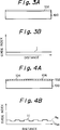
- FIG. 3A is a cross sectional view of a substrate on which an optical waveguide is formed
- FIG. 3B is a graph correspondingly plotting the distribution of a guide index of the optical waveguide shown in FIG. 3A
- FIG. 4A is a cross sectional view of a substrate on which an optical waveguide is formed, showing domain inversion regions formed in the optical waveguide
- FIG. 4B is a graph also correspondingly illustrating the distribution of a guide index of the optical waveguide having domain inversion regions.
- a planar type quasi-phase matching element includes a LiNbO3 substrate 100 on which an optical waveguide 102 is formed by a proton exchange method or the like, FIG. 3A.
- the guide index of the optical waveguide 102 is higher than that of the substrate 100 itself, and is constant from one end to another of the optical waveguide 102 as plotted with a solid line I in FIG. 3B.
- the polarized wave described above is induced in a LiNbO3 crystal, particularly, in an optical waveguide formed on +C surface of the LiNbO3, by photoelectric field of the fundamental light. It is known that the sign of the induced polarized wave can be inverted by inverting the domain in the crystal, see E.J. Lim et al, Electronic Letters, Vol. 25, No. 11, pp. 731-732 (1989).
- the domain inversion region 104 on the +C surface of the LiNbO3 substrate 100 is formed by diffusing Ti at a temperature on the order of 1,100°C, see Shintaro Miyazawa, "Ferroelectric Domain Inversion in Ti-diffused LiNbO3 Optical Waveguide” Journal of Applied Physics, Vol. 50, No. 7, pp. 4599-4603 (1979).
- the Ti diffusion concentration used here is by about 1/10 as low compared with the diffusion concentration of Ti diffused upon the formation of an optical waveguide by diffusion of Ti on the LiNbO3 substrate 100.
- the guide index of the domain inversion regions 104 becomes higher, though slightly, than that of the domain non-inversion regions 106, where domains have not been inverted, of the optical waveguide 102 even in a Ti diffusion concentration which will cause domain inversion.
- the state of variation or distribution of the guide index of the optical waveguide 102 is shown with a solid line in FIG. 4B. Therefore, this periodical domain inversion structure can be deemed as a diffraction grating whose guide index varies in the same period as that of the domain inversion structure.
- the fundamental light and SH light propagating in the quasi-phase matching element are under optical effects such as reflection or transmission by the diffractive grating.
- the periodical domain inversion structure in the quasi-phase matching element constitutes a periodical guide index distribution structure.
- the second harmonic generator of the present invention has a construction positively utilizing such a periodical guide index distribution structure formed in the optical waveguide. Then, in order to positively utilize the periodical guide index distribution structure, in the instant embodiment of the present invention, the periodical guide index distribution structure is formed as a structure which strongly reflects the fundamental wave, and the HR coating film 38 (the first chip end 34) of the LD chip 30 shown in FIG. 2 and the periodical guide index distribution structure are combined to form an external laser resonator to enable lasing.
- the oscillation wavelength of the LD chip 30 is unequivocally determined by the period of variation of guide index of the periodical guide index distribution structure 70.
- the quasi-phase matching element 50 satisfies its quasi-phase matching conditions completely and SH light can be extracted at a high efficiency.
- FIG. 5 is a graph illustrating a guide index-wavelength dispersion characteristics of LiNbO3 used as a substrate in the quasi-phase matching element according to the instant embodiment of the present invention, with horizontal axis indicating wavelength in microns and vertical axis guide index.
- n2( ⁇ ) 4.5820- ⁇ 0.099169/[(0.044432- ⁇ 2)] ⁇ - 0.021950 ⁇ 2
- FIG. 6 is a graph plotting a relationship between wavelength of a fundamental wave light (fundamental light) vs. length Lc which is by an odd number as large as coherence length lc and L( ⁇ ), with horizontal axis indicating wavelength and vertical axis L( ⁇ ) both in microns.
- FIG. 7 is a graph in which plotted is a relationship between wavelengths of a fundamental wave light (fundamental light) and of a second harmonic, vs. length Lc which is by an odd number as large as coherence length lc and L(2 ⁇ ), with horizontal axis indicating wavelength and vertical axis L(2 ⁇ ) both in microns.
- the guide indices n( ⁇ ) and n(2 ⁇ ) of LiNbO3 are replaced by effective indices N( ⁇ ) and N(2 ⁇ ) of the optical waveguide since the fundamental light and second harmonic propagate in the optical waveguide formed on the substrate. It should be noted that this replacement of guide indices will make no difference in the essence of explanation on the periodical structure.
- the effective guide indices N( ⁇ ) and N(2 ⁇ ) are guide indices for extraordinary lights since only extraordinary lights can propagate in the optical waveguide formed by the proton exchange method.
- the direction of vibration of an electric field component of an extraordinary light is substantially perpendicular to the +C surface of the LiNbO3 substrate.
- period ⁇ of variation of guide index satisfying the aforementioned three conditions:
- self quasi-phase matching method a quasi-phase matching method in which lasing is performed with light fed back from a quasi-phase matching element with suppressing lasing by a laser device by itself giving a fundamental wave light source to thereby obtain a fundamental light automatically satisfying quasi-phase matching conditions and achieve quasi-phase matching.
- values of q are indicated for every another curve. From the results a candidate value for achieving self quasi-phase matching can be obtained by extracting intersections of the group of curves satisfying the reflection conditions and the curve Lc.
- period ⁇ for a case where an AlGaAs semiconductor laser is used and the wavelength ⁇ ( ⁇ ) of the fundamental wave is set up at 830 nm.
- the effective guide indices of the optical waveguide for a wavelength ⁇ ( ⁇ ) of a fundamental wave and a wavelength ⁇ (2 ⁇ ) for second harmonic are N( ⁇ ) and N(2 ⁇ ), respectively.
- N( ⁇ ) 2.1727
- N(2 ⁇ ) 2.3139
- the quasi-phase matching element 50 efficiently generates a second harmonic light using the laser beam at this oscillation wavelength as a fundamental wave light, with the second harmonic light being emitted from the quasi-phase matching element 50 at an increased light intensity and at a high power with substantially no reflection.
- the second harmonic generator includes the LD chip 30 and SHG element 50 arranged in such a manner that the fundamental light can enter substantially perpendicularly to the first element end 58. Therefore, there is a high possibility that a reflected light from the first element end 58 reenters the LD chip 30, and there is a fear that sometimes the oscillation conditions of the laser diode cannot be determined by the HR coating surface (the first chip end) 34 and the period ⁇ of the guide index distribution structure alone. Furthermore, it is difficult to coat a antireflection film on the first and second element ends 58 and 60 of the SHG element 50. Fortunately, however, it is easy to polish ends of a crystal substrate made of LiNbO3, for example.
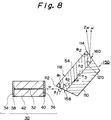
- FIG. 8 is a schematic cross sectional view of a second harmonic generator according to anther embodiment of the present invention, showing an arrangement of an LD chip and an SHG element corresponding to one shown in FIG. 2.
- FIG. 9 is a schematic perspective view of an second harmonic generating element corresponding to one shown in FIG. 1, schematically illustrating its specific construction.
- the LD chip and SHG element themselves used in the instant embodiment are the same in construction as the LD chip 30 and the SHG element 50 used in the arrangement shown in FIG. 2 and the like components are designated by the same reference numerals and detailed description thereon is omitted here but differences in the construction therebetween will be described in the main.
- the LD chip 30 and the SHG element 50 are arranged so that the fundamental wave light from the LD chip 30 can be incident into the optical waveguide 54 of the SHG element 150 at the Brewster angle or at an angle approximate thereto;
- Interior angles ⁇ I and ⁇ 2 between the first and second element ends 158 and 160, respectively, and the +C face (surface) of the crystal substrate 118 are not 90°.
- a crystal substrate 110 is a LiNbO3 substrate and its surface 118 is +C face (also referred to as Z face).
- SHG element 150 the first element face 158 which is the incident and emerging end of a fundamental wave light is inclined relative to the +C face 118 at an interior angle of ⁇ 1 ( ⁇ 90°), and the second element end 160 serving as an emerging face for SH light is similarly inclined relative to the +C face 118 at an interior angle of ⁇ 2 ( ⁇ 90°).
- ⁇ 1 ⁇ 2.
- the first and second element ends 158 and 160 are formed by polishing the substrate 100. Edges 112 and 114 formed between the first and second element ends 158 and 160, respectively, and the +C face 118 are parallel to each other.
- the optical waveguide 54 extends in a surface region of the +C face 118 between the first and second element ends 158 and 160.
- the direction of extension (X direction) is substantially perpendicular to the edges 112 and 114.
- An interface 120 between the optical waveguide 54 and the remaining LiNbO3 region is parallel to the +C face 118. Therefore, incident light into the SHG element and emerging light from the SHG element exist in the same plane. For the remaining points, the same description as made with reference to FIGS. 1 through FIGS. 4A and 4B will be applicable and will not be repeated here.
- the first element end 158 is inclined relative to the +C face at an inclination angle of ⁇ 1, which enables introduction of a light (fundamental light) emerging from the LD chip 30 on the incident face 158 being the first element end at the Brewster angle ⁇ 1 and also propagation of the light (fundamental light) incident into the optical waveguide 54 in the optical waveguide in a guided mode.
- n2 guide index of the optical waveguide for the fundamental light
- n3 guide index of LiNbO3 for the fundamental light.
- the Brewster angle ⁇ 1 may be set up at several values in the vicinity of an intended wavelength an optimal combination may be chosen in a stage of integrating the LD chip and the SHG element.
- conditions for ⁇ 1 are considerably loose and deviation of incident angle ⁇ of the fundamental light from ⁇ 1 by a few degrees causes no reflection on the incident and emerging face. That is, of the light from the active layer 32 of the LD chip 30, a light component linearly polarized in a direction substantially parallel to the plane of the figure enters the optical waveguide 54 with substantially no reflection on the first element end.
- the SHG element 150 is shown as being arranged perpendicular to the +C face 118 of the LiNbO3 substrate 110 and in the direction in which the optical waveguide 54 extends, expressed in cross section in a plane passing through the optical waveguide 54.
- the SHG element 150 originally has a long distance between the first and second element ends as shown in FIG. 9, but in FIG. 8 it is shown schematically with its length being reduced.
- the LD chip 30 is arranged in FIG. 8 such that the direction of vibration of the electric field of the emerging light or p-polarized light is parallel to the plane of the figure.
- the fundamental light or p-polarized light enters into the optical waveguide 54 without being reflected at the incident face 158 which is the first element end.
- the fundamental light and SH light are emitted through the emerging end 160 without being reflected thereon.
- the s-polarized light is totally reflected at the incident face 158 and will not return to the LD chip 30 side.
- the wavelength of the generated light from the LD chip 30 is determined depending on the HR coating surface 34 and the periodical guide index distribution structure 70 in the optical waveguide 54.
- the LD chip 30 and the SHG element 150 can be arranged so that a desired fundamental light can be obtained with adjustment of the incident angle ⁇ by polishing without strict AR coating treatment of the incident and emerging end 158 of the SHG element 150.
- Conditions which the interior angle ⁇ 1 has to satisfy in order to permit the fundamental light satisfying the Brewster condition to propagate or be guided in the optical waveguide 54 are specifically obtained as follows.
- the wavelength ⁇ ( ⁇ ) of the fundamental light is set up at 830 nm.
- the incident fundamental light which was incident at an incident angle ⁇ being equal to the Brewster angle ⁇ 1 and entered into the optical waveguide 54 at a refractive angle ⁇ 2 satisfy complete reflection conditions at point P on the interface 120 between the LiNbO3 substrate 100 and the optical waveguide 54. If the conditions are met, the conditions of complete reflection at the +C face, which is an interface between the optical waveguide and air, are automatically satisfied.
- ⁇ 1 has to be set up in the range of: 49.2° ⁇ ⁇ 1 ⁇ 83.3°, in order to satisfy desired conditions.
- the embodiment shown in FIG. 8 can realize with ease the quasi-phase matching that was difficult to attain conventionally, thus enabling fabrication of an SH generator with a high conversion efficiency.
- the second harmonic generator in accordance with the present invention is of a construction including a semiconductor laser chip and a quasi-phase matching element optically coupled together and capable of realizing second harmonic generation (SHG) by automatically obtaining a wavelength of fundamental wave light which enables quasi-phase matching, i.e. self quasi-phase matching.
- the emerging end of the semiconductor laser chip is provided with a low reflection coating (AR coating) to put it in a state in which the lasing of the semiconductor laser by itself is suppressed and the semiconductor laser is automatically activated by a light fed back from the optical waveguide in the quasi-phase matching element at a wavelength which satisfies the quasi-phase matching conditions of the quasi-phase matching element.
- the generated laser beam is introduced into the quasi-phase matching element as a fundamental wave light to generate the second harmonic in the quasi-phase matching element.
- the periodical domain inversion structure is formed by diffusing Ti in an optical waveguide provided in a LiNBO3 substrate.
- the Ti-diffused domain inversion regions have guide indices slightly higher than the guide indices of the non-domain inverted regions (domain non-inversion regions), resulting in that the periodically arranged domain inversion regions form a reflection type diffraction grating, thus coinciding with the periodical guide index distribution structure.
- the wavelength of a light reflected by the periodical guide index distribution structure is determined by the period of the domain inversion regions.
- the period of the inversion structure is determined so as to satisfy the quasi-phase matching conditions and the reflection conditions of the fundamental light as well, thus arranging the quasi-phase matching element and the semiconductor laser chip in optical coupling such that the light fed back from the quasi-phase matching element can be returned into the active layer of the semiconductor laser in order to realize second harmonic generation based on self quasi-phase matching.
- the quasi-phase matching element use is made of a planar type element as the quasi-phase matching element, and the LD chip and quasi-phase matching element are arranged so that the fundamental wave light can enter the first element end at right angles.
- the LD chip and the quasi-phase matching element are arranged so that the fundamental wave light can be incident at the Brewster angle.
- the present invention is not limited to the illustrative embodiments described above and shown in the drawings, and it is obvious to one skilled in the art that various modification or variation may be made thereto.
- the periodical domain inversion structure and the periodical guide index distribution structure may differ from one another and any type of quasi-phase matching element may be used so far as it has a periodical guide index distribution structure in the optical waveguide in contrast to the preceding embodiments in which the both structures coincide with each other.
- the quasi-phase matching element is made of LiNbO3 crystal in the aforementioned embodiments
- KTP instead of LiNbO3 crystal may be used for forming the element.
- optical waveguide in the quasi-phase matching element is formed by a proton exchange method in the aforementioned embodiments
- an optical waveguide formed on a substrate material by any suitable method may be used.
- an optical waveguide cannot be formed on a LiNbO3 substrate by the Ti diffusion method because the method gives domain inversion regions throughout the optical waveguide but fails to provide a periodical domain inversion structure.
- an optical waveguide may preferably be formed by an Li+ - H+ exchange method usually used after the formation of domain inversion regions.
- the domain inversion regions are formed by Ti diffusion on a LiNbO3 substrate but external diffusion of LiO2 may also be used instead of Ti diffusion.
- the fundamental wave light of the SHG element used in the second harmonic generator has a wavelength in the range of gain of the semiconductor laser chip used. While in the aforementioned embodiments, description has been made by setting up the wavelength of the fundamental wave light at 830 nm, fundamental wave lights having other wavelengths can also be generated. In this case, numerical conditions used or obtained in the aforementioned embodiments are varied. Of course such numerical conditions may vary depending on materials used for the substrate of an SHG element and for the optical waveguide. Furthermore, the semiconductor laser chip may be other than AlGaAs type ones, for example, InGaAs, InGaAsP or other InAs type semiconductor laser chips.
- this element may also be formed in the form of an optical fiber, with forming a core serving as an optical waveguide so as to have a structure in which guide index varies periodically (periodical guide index distribution structure) and making higher guide index portions and lower guide index portions to have different diameters from one another.
- An example of such an optical fiber type of quasi-phase matching element is shown in FIG. 10.
- a quasi-phase matching element 80 may be constructed to include, for example, a core 82 made of LiNbO3, a clad made of suitable material and provided around the core 82 and having a guide index lower than that of the core 82, the core 82 having periodically a higher and a lower guide index regions 86 and 88, thus forming a periodical guide index distribution structure.
- the lengths of the higher and lower guide index regions, respectively may be set up at coherence length or a length by an odd number as large as the coherence length. This construction allows the second harmonic to increase period after period (for every 2 lc) in accordance with the difference between the generation efficiency of the second harmonic in the lower guide index region 88 and that of the second harmonic in the higher guide index region 86.
- a 1/2 wavelength plate 72 is inserted between the semiconductor laser chip 30 and the quasi-phase matching element 50.
- the use of the 1/2 wavelength plate 72 is to realize an efficient introduction of the emerging light from the active layer 32 of the semiconductor laser into the optical waveguide 54 in the quasi-phase matching element 50.
- the plate 72 may be omitted.
Landscapes
- Physics & Mathematics (AREA)
- Nonlinear Science (AREA)
- General Physics & Mathematics (AREA)
- Optics & Photonics (AREA)
- Condensed Matter Physics & Semiconductors (AREA)
- Electromagnetism (AREA)
- Optical Modulation, Optical Deflection, Nonlinear Optics, Optical Demodulation, Optical Logic Elements (AREA)
- Semiconductor Lasers (AREA)
- Lasers (AREA)
- Optical Integrated Circuits (AREA)
Applications Claiming Priority (6)
| Application Number | Priority Date | Filing Date | Title |
|---|---|---|---|
| JP301925/90 | 1990-11-07 | ||
| JP30192590 | 1990-11-07 | ||
| JP2994691 | 1991-02-25 | ||
| JP29946/91 | 1991-02-25 | ||
| JP51930/91 | 1991-03-18 | ||
| JP3051930A JP2721436B2 (ja) | 1990-11-07 | 1991-03-18 | 第2高調波発生装置 |
Publications (3)
| Publication Number | Publication Date |
|---|---|
| EP0485187A2 true EP0485187A2 (de) | 1992-05-13 |
| EP0485187A3 EP0485187A3 (en) | 1993-02-10 |
| EP0485187B1 EP0485187B1 (de) | 1996-05-08 |
Family
ID=27286778
Family Applications (1)
| Application Number | Title | Priority Date | Filing Date |
|---|---|---|---|
| EP91310248A Expired - Lifetime EP0485187B1 (de) | 1990-11-07 | 1991-11-06 | Vorrichtung zur Erzeugung der zweiten Harmonischen einer von einer Laserquelle erzeugten Grundschwingung |
Country Status (4)
| Country | Link |
|---|---|
| US (1) | US5247528A (de) |
| EP (1) | EP0485187B1 (de) |
| JP (1) | JP2721436B2 (de) |
| DE (1) | DE69119360T2 (de) |
Cited By (7)
| Publication number | Priority date | Publication date | Assignee | Title |
|---|---|---|---|---|
| EP0559139A1 (de) * | 1992-03-03 | 1993-09-08 | Matsushita Electric Industrial Co., Ltd. | Vorrichtung zur Erzeugung von Licht mit kurzer Wellenlänge |
| EP0632553A3 (de) * | 1993-06-30 | 1995-01-25 | Hewlett Packard Co | |
| US5422903A (en) * | 1993-04-15 | 1995-06-06 | Yamada; Norihide | Surface emitting second harmonic generating device |
| GB2343964A (en) * | 1998-11-03 | 2000-05-24 | Toshiba Res Europ Ltd | A non linear optical device with a varied refractive index |
| US6388799B1 (en) * | 1998-11-03 | 2002-05-14 | Toshiba Research Europe Limited | Optical device and imaging system |
| WO2002025782A3 (en) * | 2000-09-22 | 2003-09-25 | Blue Leaf Inc | Optical transmitter comprising a stepwise tunable laser |
| KR100701541B1 (ko) * | 1999-06-30 | 2007-03-30 | 로베르트 보쉬 게엠베하 | Cvt의 변속비를 유압식으로 조정하기 위한 시스템 |
Families Citing this family (33)
| Publication number | Priority date | Publication date | Assignee | Title |
|---|---|---|---|---|
| DE69327352T3 (de) * | 1992-10-07 | 2007-06-06 | Matsushita Electric Industrial Co., Ltd., Kadoma | Optische Wellenlängenwandlervorrichtung zur Erzeugung der zweiten Harmonischen |
| US5355247A (en) * | 1993-03-30 | 1994-10-11 | The Board Of Trustees Of The Leland Stanford, Jr. University | Method using a monolithic crystalline material for producing radiation by quasi-phase-matching, diffusion bonded monolithic crystalline material for quasi-phase-matching, and method for fabricating same |
| US5390210A (en) * | 1993-11-22 | 1995-02-14 | Hewlett-Packard Company | Semiconductor laser that generates second harmonic light with attached nonlinear crystal |
| DE4416607C2 (de) * | 1994-05-11 | 1997-09-04 | Klaus Reimann | Vorrichtung zur Verdopplung der Laserfrequenz einer Halbleiterlaserdiode |
| US5544271A (en) * | 1994-12-12 | 1996-08-06 | Uniphase Corporation | Nonlinear optical generator with index of refraction perturbed reflector arrangement |
| JP3767927B2 (ja) * | 1995-01-31 | 2006-04-19 | 沖電気工業株式会社 | 波長変換方法及びそれを用いた波長変換装置 |
| GB2300964B (en) * | 1995-05-13 | 1999-11-10 | I E Optomech Limited | Monolithic laser |
| JPH09146128A (ja) * | 1995-11-24 | 1997-06-06 | Sony Corp | 電気光学素子 |
| US5787102A (en) * | 1996-11-20 | 1998-07-28 | Lightwave Electronics Corporation | Light generating device and method using a periodically structured non-linear material and orthogonal optical interaction |
| US5987041A (en) * | 1997-04-23 | 1999-11-16 | Mitsubishi Cable Industries, Ltd. | Laser apparatus and method for emission of laser beam using same |
| US6262830B1 (en) | 1997-09-16 | 2001-07-17 | Michael Scalora | Transparent metallo-dielectric photonic band gap structure |
| US5907427A (en) | 1997-10-24 | 1999-05-25 | Time Domain Corporation | Photonic band gap device and method using a periodicity defect region to increase photonic signal delay |
| US6122299A (en) * | 1997-12-31 | 2000-09-19 | Sdl, Inc. | Angled distributed reflector optical device with enhanced light confinement |
| US6304366B1 (en) * | 1998-04-02 | 2001-10-16 | Michael Scalora | Photonic signal frequency conversion using a photonic band gap structure |
| US6744552B2 (en) * | 1998-04-02 | 2004-06-01 | Michael Scalora | Photonic signal frequency up and down-conversion using a photonic band gap structure |
| US6711183B1 (en) | 1998-05-18 | 2004-03-23 | Matsushita Electric Industrial Co., Ltd. | Optical wavelength conversion device, coherent light generator, and optical information processing apparatus |
| US6396617B1 (en) | 1999-05-17 | 2002-05-28 | Michael Scalora | Photonic band gap device and method using a periodicity defect region doped with a gain medium to increase photonic signal delay |
| US6538794B1 (en) | 1999-09-30 | 2003-03-25 | D'aguanno Giuseppe | Efficient non-linear phase shifting using a photonic band gap structure |
| US6414780B1 (en) | 1999-12-23 | 2002-07-02 | D'aguanno Giuseppe | Photonic signal reflectivity and transmissivity control using a photonic band gap structure |
| US6339493B1 (en) | 1999-12-23 | 2002-01-15 | Michael Scalora | Apparatus and method for controlling optics propagation based on a transparent metal stack |
| JP2003015175A (ja) * | 2001-04-27 | 2003-01-15 | Mitsubishi Electric Corp | 固体光源装置 |
| US7088877B2 (en) | 2001-06-13 | 2006-08-08 | Intel Corporation | Method and apparatus for tuning a bragg grating in a semiconductor substrate |
| US6950577B2 (en) * | 2002-07-01 | 2005-09-27 | Intel Corporation | Waveguide-based Bragg gratings with spectral sidelobe suppression and method thereof |
| US7245792B2 (en) * | 2002-08-16 | 2007-07-17 | Intel Corporation | Silicon-based tunable single passband optical filter |
| US7190706B2 (en) * | 2003-12-10 | 2007-03-13 | Avago Technologies Fiber Ip (Singapore) Ptd. Ltd. | Soft metal heat transfer for transceivers |
| JP4636315B2 (ja) * | 2004-04-22 | 2011-02-23 | ソニー株式会社 | 1次元照明装置及び画像生成装置 |
| WO2007013513A1 (ja) * | 2005-07-28 | 2007-02-01 | Matsushita Electric Industrial Co., Ltd. | 波長変換素子、レーザ光源装置、2次元画像表示装置及びレーザ加工装置 |
| US7826500B2 (en) | 2005-08-29 | 2010-11-02 | Panasonic Corporation | Fiber laser and optical device |
| US8038305B2 (en) * | 2007-02-07 | 2011-10-18 | Seiko Epson Corporation | Light source unit, illumination device, image display apparatus, and monitor apparatus |
| JP2008311601A (ja) * | 2007-06-18 | 2008-12-25 | Motohiko Inai | 固体青色レーザー装置 |
| DE102008052376A1 (de) * | 2008-10-20 | 2010-04-22 | Osram Opto Semiconductors Gmbh | Laseranordnung |
| US8111452B2 (en) * | 2010-02-22 | 2012-02-07 | Corning Incorporated | Wavelength conversion device with microlens and optical package incorporating the same |
| DE102018129623A1 (de) * | 2018-11-23 | 2020-05-28 | Forschungsverbund Berlin E.V. | Vorrichtung zur Erzeugung von Laserstrahlung |
Family Cites Families (5)
| Publication number | Priority date | Publication date | Assignee | Title |
|---|---|---|---|---|
| US4731787A (en) * | 1986-08-15 | 1988-03-15 | Board Of Trustees, Stanford University | Monolithic phasematched laser harmonic generator |
| JPH01134984A (ja) * | 1987-11-19 | 1989-05-26 | Mitsubishi Electric Corp | 半導体レーザ装置 |
| US4930132A (en) * | 1987-12-28 | 1990-05-29 | Canon Kabushiki Kaisha | Second harmonic wave generating device having active layer and second harmonic wave generating layer on same substrate |
| JPH03251826A (ja) * | 1990-01-25 | 1991-11-11 | Oki Electric Ind Co Ltd | 第2高調波発生素子 |
| US5038352A (en) * | 1990-11-13 | 1991-08-06 | International Business Machines Incorporation | Laser system and method using a nonlinear crystal resonator |
-
1991
- 1991-03-18 JP JP3051930A patent/JP2721436B2/ja not_active Expired - Fee Related
- 1991-11-05 US US07/787,939 patent/US5247528A/en not_active Expired - Lifetime
- 1991-11-06 DE DE69119360T patent/DE69119360T2/de not_active Expired - Lifetime
- 1991-11-06 EP EP91310248A patent/EP0485187B1/de not_active Expired - Lifetime
Cited By (11)
| Publication number | Priority date | Publication date | Assignee | Title |
|---|---|---|---|---|
| EP0559139A1 (de) * | 1992-03-03 | 1993-09-08 | Matsushita Electric Industrial Co., Ltd. | Vorrichtung zur Erzeugung von Licht mit kurzer Wellenlänge |
| US5301059A (en) * | 1992-03-03 | 1994-04-05 | Matsushita Electric Industrial Co., Ltd. | Short-wavelength light generating apparatus |
| US5422903A (en) * | 1993-04-15 | 1995-06-06 | Yamada; Norihide | Surface emitting second harmonic generating device |
| EP0632553A3 (de) * | 1993-06-30 | 1995-01-25 | Hewlett Packard Co | |
| GB2343964A (en) * | 1998-11-03 | 2000-05-24 | Toshiba Res Europ Ltd | A non linear optical device with a varied refractive index |
| GB2347756A (en) * | 1998-11-03 | 2000-09-13 | Toshiba Res Europ Ltd | A radiation source with frequency conversion member and imaging system |
| GB2343964B (en) * | 1998-11-03 | 2000-11-01 | Toshiba Res Europ Ltd | An optical device |
| GB2347756B (en) * | 1998-11-03 | 2001-08-01 | Toshiba Res Europ Ltd | A radiation source and imaging system |
| US6388799B1 (en) * | 1998-11-03 | 2002-05-14 | Toshiba Research Europe Limited | Optical device and imaging system |
| KR100701541B1 (ko) * | 1999-06-30 | 2007-03-30 | 로베르트 보쉬 게엠베하 | Cvt의 변속비를 유압식으로 조정하기 위한 시스템 |
| WO2002025782A3 (en) * | 2000-09-22 | 2003-09-25 | Blue Leaf Inc | Optical transmitter comprising a stepwise tunable laser |
Also Published As
| Publication number | Publication date |
|---|---|
| JP2721436B2 (ja) | 1998-03-04 |
| US5247528A (en) | 1993-09-21 |
| EP0485187A3 (en) | 1993-02-10 |
| JPH06283791A (ja) | 1994-10-07 |
| DE69119360T2 (de) | 1997-01-02 |
| DE69119360D1 (de) | 1996-06-13 |
| EP0485187B1 (de) | 1996-05-08 |
Similar Documents
| Publication | Publication Date | Title |
|---|---|---|
| EP0485187B1 (de) | Vorrichtung zur Erzeugung der zweiten Harmonischen einer von einer Laserquelle erzeugten Grundschwingung | |
| EP0712183A2 (de) | Wellenlängenstabilisierter Lichtquelle | |
| JP2892938B2 (ja) | 波長変換装置 | |
| US5617435A (en) | Lasing system with wavelength-conversion waveguide | |
| US5504616A (en) | Wavelength conversion device | |
| JPH05333395A (ja) | 光波長変換装置 | |
| JP2685969B2 (ja) | 第2高調波発生装置 | |
| US5109462A (en) | Light wavelength converter | |
| JPH10254001A (ja) | 光波長変換モジュール | |
| JP3129028B2 (ja) | 短波長レーザ光源 | |
| JP3156444B2 (ja) | 短波長レーザ光源およびその製造方法 | |
| US5615042A (en) | Compact optical source based on the frequency doubling of a laser and self-stabilized by the depletion of the pump | |
| JP3187290B2 (ja) | 波長変換装置および波長変換方法 | |
| JP3111786B2 (ja) | 短波長レーザ光源 | |
| JP2000286498A (ja) | 半導体レーザモジュール、及び半導体レーザモジュールの作成方法 | |
| JP2822778B2 (ja) | 波長変換素子 | |
| EP0450557B1 (de) | Wellenlängenwandler für Laserlicht | |
| JP2643735B2 (ja) | 波長変換素子 | |
| JPH0651359A (ja) | 波長変換素子、短波長レーザ装置および波長可変レーザ装置 | |
| JP2658381B2 (ja) | 導波路型波長変換素子 | |
| JP2982366B2 (ja) | 導波路型波長変換素子 | |
| JP2000267146A (ja) | 導波路型光変調素子及び波長変換装置 | |
| JP2004020571A (ja) | 波長変換装置 | |
| JPH0736071A (ja) | 波長変換装置 | |
| JP2000314903A (ja) | 光波長変換モジュールの作製方法及び光波長変換モジュール |
Legal Events
| Date | Code | Title | Description |
|---|---|---|---|
| PUAI | Public reference made under article 153(3) epc to a published international application that has entered the european phase |
Free format text: ORIGINAL CODE: 0009012 |
|
| AK | Designated contracting states |
Kind code of ref document: A2 Designated state(s): DE FR GB SE |
|
| PUAL | Search report despatched |
Free format text: ORIGINAL CODE: 0009013 |
|
| AK | Designated contracting states |
Kind code of ref document: A3 Designated state(s): DE FR GB SE |
|
| 17P | Request for examination filed |
Effective date: 19930504 |
|
| 17Q | First examination report despatched |
Effective date: 19950213 |
|
| GRAH | Despatch of communication of intention to grant a patent |
Free format text: ORIGINAL CODE: EPIDOS IGRA |
|
| GRAA | (expected) grant |
Free format text: ORIGINAL CODE: 0009210 |
|
| AK | Designated contracting states |
Kind code of ref document: B1 Designated state(s): DE FR GB SE |
|
| REF | Corresponds to: |
Ref document number: 69119360 Country of ref document: DE Date of ref document: 19960613 |
|
| ET | Fr: translation filed | ||
| PLBE | No opposition filed within time limit |
Free format text: ORIGINAL CODE: 0009261 |
|
| STAA | Information on the status of an ep patent application or granted ep patent |
Free format text: STATUS: NO OPPOSITION FILED WITHIN TIME LIMIT |
|
| 26N | No opposition filed | ||
| REG | Reference to a national code |
Ref country code: GB Ref legal event code: IF02 |
|
| PGFP | Annual fee paid to national office [announced via postgrant information from national office to epo] |
Ref country code: DE Payment date: 20091029 Year of fee payment: 19 Ref country code: SE Payment date: 20091106 Year of fee payment: 19 |
|
| PGFP | Annual fee paid to national office [announced via postgrant information from national office to epo] |
Ref country code: FR Payment date: 20091123 Year of fee payment: 19 Ref country code: GB Payment date: 20091104 Year of fee payment: 19 |
|
| REG | Reference to a national code |
Ref country code: SE Ref legal event code: EUG |
|
| GBPC | Gb: european patent ceased through non-payment of renewal fee |
Effective date: 20101106 |
|
| REG | Reference to a national code |
Ref country code: FR Ref legal event code: ST Effective date: 20110801 |
|
| REG | Reference to a national code |
Ref country code: DE Ref legal event code: R119 Ref document number: 69119360 Country of ref document: DE Effective date: 20110601 Ref country code: DE Ref legal event code: R119 Ref document number: 69119360 Country of ref document: DE Effective date: 20110531 |
|
| PG25 | Lapsed in a contracting state [announced via postgrant information from national office to epo] |
Ref country code: DE Free format text: LAPSE BECAUSE OF NON-PAYMENT OF DUE FEES Effective date: 20110531 Ref country code: SE Free format text: LAPSE BECAUSE OF NON-PAYMENT OF DUE FEES Effective date: 20101107 |
|
| PG25 | Lapsed in a contracting state [announced via postgrant information from national office to epo] |
Ref country code: FR Free format text: LAPSE BECAUSE OF NON-PAYMENT OF DUE FEES Effective date: 20101130 |
|
| PG25 | Lapsed in a contracting state [announced via postgrant information from national office to epo] |
Ref country code: GB Free format text: LAPSE BECAUSE OF NON-PAYMENT OF DUE FEES Effective date: 20101106 |