EP0472221B1 - Méthode pour la fabrication d'un dispositif optique à semi-conducteur - Google Patents
Méthode pour la fabrication d'un dispositif optique à semi-conducteur Download PDFInfo
- Publication number
- EP0472221B1 EP0472221B1 EP91114272A EP91114272A EP0472221B1 EP 0472221 B1 EP0472221 B1 EP 0472221B1 EP 91114272 A EP91114272 A EP 91114272A EP 91114272 A EP91114272 A EP 91114272A EP 0472221 B1 EP0472221 B1 EP 0472221B1
- Authority
- EP
- European Patent Office
- Prior art keywords
- layer
- sio2
- inp
- stripes
- width
- Prior art date
- Legal status (The legal status is an assumption and is not a legal conclusion. Google has not performed a legal analysis and makes no representation as to the accuracy of the status listed.)
- Expired - Lifetime
Links
Images


Classifications
-
- B—PERFORMING OPERATIONS; TRANSPORTING
- B82—NANOTECHNOLOGY
- B82Y—SPECIFIC USES OR APPLICATIONS OF NANOSTRUCTURES; MEASUREMENT OR ANALYSIS OF NANOSTRUCTURES; MANUFACTURE OR TREATMENT OF NANOSTRUCTURES
- B82Y20/00—Nanooptics, e.g. quantum optics or photonic crystals
-
- H—ELECTRICITY
- H01—ELECTRIC ELEMENTS
- H01L—SEMICONDUCTOR DEVICES NOT COVERED BY CLASS H10
- H01L33/00—Semiconductor devices with at least one potential-jump barrier or surface barrier specially adapted for light emission; Processes or apparatus specially adapted for the manufacture or treatment thereof or of parts thereof; Details thereof
- H01L33/005—Processes
- H01L33/0062—Processes for devices with an active region comprising only III-V compounds
-
- H—ELECTRICITY
- H01—ELECTRIC ELEMENTS
- H01S—DEVICES USING THE PROCESS OF LIGHT AMPLIFICATION BY STIMULATED EMISSION OF RADIATION [LASER] TO AMPLIFY OR GENERATE LIGHT; DEVICES USING STIMULATED EMISSION OF ELECTROMAGNETIC RADIATION IN WAVE RANGES OTHER THAN OPTICAL
- H01S3/00—Lasers, i.e. devices using stimulated emission of electromagnetic radiation in the infrared, visible or ultraviolet wave range
- H01S3/10—Controlling the intensity, frequency, phase, polarisation or direction of the emitted radiation, e.g. switching, gating, modulating or demodulating
- H01S3/105—Controlling the intensity, frequency, phase, polarisation or direction of the emitted radiation, e.g. switching, gating, modulating or demodulating by controlling the mutual position or the reflecting properties of the reflectors of the cavity, e.g. by controlling the cavity length
- H01S3/1055—Controlling the intensity, frequency, phase, polarisation or direction of the emitted radiation, e.g. switching, gating, modulating or demodulating by controlling the mutual position or the reflecting properties of the reflectors of the cavity, e.g. by controlling the cavity length one of the reflectors being constituted by a diffraction grating
-
- H—ELECTRICITY
- H01—ELECTRIC ELEMENTS
- H01S—DEVICES USING THE PROCESS OF LIGHT AMPLIFICATION BY STIMULATED EMISSION OF RADIATION [LASER] TO AMPLIFY OR GENERATE LIGHT; DEVICES USING STIMULATED EMISSION OF ELECTROMAGNETIC RADIATION IN WAVE RANGES OTHER THAN OPTICAL
- H01S5/00—Semiconductor lasers
- H01S5/02—Structural details or components not essential to laser action
- H01S5/026—Monolithically integrated components, e.g. waveguides, monitoring photo-detectors, drivers
-
- H—ELECTRICITY
- H01—ELECTRIC ELEMENTS
- H01S—DEVICES USING THE PROCESS OF LIGHT AMPLIFICATION BY STIMULATED EMISSION OF RADIATION [LASER] TO AMPLIFY OR GENERATE LIGHT; DEVICES USING STIMULATED EMISSION OF ELECTROMAGNETIC RADIATION IN WAVE RANGES OTHER THAN OPTICAL
- H01S5/00—Semiconductor lasers
- H01S5/04—Processes or apparatus for excitation, e.g. pumping, e.g. by electron beams
- H01S5/042—Electrical excitation ; Circuits therefor
- H01S5/0425—Electrodes, e.g. characterised by the structure
- H01S5/04256—Electrodes, e.g. characterised by the structure characterised by the configuration
-
- H—ELECTRICITY
- H01—ELECTRIC ELEMENTS
- H01S—DEVICES USING THE PROCESS OF LIGHT AMPLIFICATION BY STIMULATED EMISSION OF RADIATION [LASER] TO AMPLIFY OR GENERATE LIGHT; DEVICES USING STIMULATED EMISSION OF ELECTROMAGNETIC RADIATION IN WAVE RANGES OTHER THAN OPTICAL
- H01S5/00—Semiconductor lasers
- H01S5/10—Construction or shape of the optical resonator, e.g. extended or external cavity, coupled cavities, bent-guide, varying width, thickness or composition of the active region
- H01S5/11—Comprising a photonic bandgap structure
-
- H—ELECTRICITY
- H01—ELECTRIC ELEMENTS
- H01S—DEVICES USING THE PROCESS OF LIGHT AMPLIFICATION BY STIMULATED EMISSION OF RADIATION [LASER] TO AMPLIFY OR GENERATE LIGHT; DEVICES USING STIMULATED EMISSION OF ELECTROMAGNETIC RADIATION IN WAVE RANGES OTHER THAN OPTICAL
- H01S5/00—Semiconductor lasers
- H01S5/20—Structure or shape of the semiconductor body to guide the optical wave ; Confining structures perpendicular to the optical axis, e.g. index or gain guiding, stripe geometry, broad area lasers, gain tailoring, transverse or lateral reflectors, special cladding structures, MQW barrier reflection layers
- H01S5/22—Structure or shape of the semiconductor body to guide the optical wave ; Confining structures perpendicular to the optical axis, e.g. index or gain guiding, stripe geometry, broad area lasers, gain tailoring, transverse or lateral reflectors, special cladding structures, MQW barrier reflection layers having a ridge or stripe structure
- H01S5/227—Buried mesa structure ; Striped active layer
-
- H—ELECTRICITY
- H01—ELECTRIC ELEMENTS
- H01S—DEVICES USING THE PROCESS OF LIGHT AMPLIFICATION BY STIMULATED EMISSION OF RADIATION [LASER] TO AMPLIFY OR GENERATE LIGHT; DEVICES USING STIMULATED EMISSION OF ELECTROMAGNETIC RADIATION IN WAVE RANGES OTHER THAN OPTICAL
- H01S5/00—Semiconductor lasers
- H01S5/02—Structural details or components not essential to laser action
- H01S5/026—Monolithically integrated components, e.g. waveguides, monitoring photo-detectors, drivers
- H01S5/0265—Intensity modulators
-
- H—ELECTRICITY
- H01—ELECTRIC ELEMENTS
- H01S—DEVICES USING THE PROCESS OF LIGHT AMPLIFICATION BY STIMULATED EMISSION OF RADIATION [LASER] TO AMPLIFY OR GENERATE LIGHT; DEVICES USING STIMULATED EMISSION OF ELECTROMAGNETIC RADIATION IN WAVE RANGES OTHER THAN OPTICAL
- H01S5/00—Semiconductor lasers
- H01S5/06—Arrangements for controlling the laser output parameters, e.g. by operating on the active medium
- H01S5/062—Arrangements for controlling the laser output parameters, e.g. by operating on the active medium by varying the potential of the electrodes
- H01S5/0625—Arrangements for controlling the laser output parameters, e.g. by operating on the active medium by varying the potential of the electrodes in multi-section lasers
- H01S5/06255—Controlling the frequency of the radiation
- H01S5/06256—Controlling the frequency of the radiation with DBR-structure
-
- H—ELECTRICITY
- H01—ELECTRIC ELEMENTS
- H01S—DEVICES USING THE PROCESS OF LIGHT AMPLIFICATION BY STIMULATED EMISSION OF RADIATION [LASER] TO AMPLIFY OR GENERATE LIGHT; DEVICES USING STIMULATED EMISSION OF ELECTROMAGNETIC RADIATION IN WAVE RANGES OTHER THAN OPTICAL
- H01S5/00—Semiconductor lasers
- H01S5/10—Construction or shape of the optical resonator, e.g. extended or external cavity, coupled cavities, bent-guide, varying width, thickness or composition of the active region
- H01S5/16—Window-type lasers, i.e. with a region of non-absorbing material between the active region and the reflecting surface
- H01S5/164—Window-type lasers, i.e. with a region of non-absorbing material between the active region and the reflecting surface with window regions comprising semiconductor material with a wider bandgap than the active layer
-
- H—ELECTRICITY
- H01—ELECTRIC ELEMENTS
- H01S—DEVICES USING THE PROCESS OF LIGHT AMPLIFICATION BY STIMULATED EMISSION OF RADIATION [LASER] TO AMPLIFY OR GENERATE LIGHT; DEVICES USING STIMULATED EMISSION OF ELECTROMAGNETIC RADIATION IN WAVE RANGES OTHER THAN OPTICAL
- H01S5/00—Semiconductor lasers
- H01S5/20—Structure or shape of the semiconductor body to guide the optical wave ; Confining structures perpendicular to the optical axis, e.g. index or gain guiding, stripe geometry, broad area lasers, gain tailoring, transverse or lateral reflectors, special cladding structures, MQW barrier reflection layers
- H01S5/2054—Methods of obtaining the confinement
- H01S5/2077—Methods of obtaining the confinement using lateral bandgap control during growth, e.g. selective growth, mask induced
-
- H—ELECTRICITY
- H01—ELECTRIC ELEMENTS
- H01S—DEVICES USING THE PROCESS OF LIGHT AMPLIFICATION BY STIMULATED EMISSION OF RADIATION [LASER] TO AMPLIFY OR GENERATE LIGHT; DEVICES USING STIMULATED EMISSION OF ELECTROMAGNETIC RADIATION IN WAVE RANGES OTHER THAN OPTICAL
- H01S5/00—Semiconductor lasers
- H01S5/20—Structure or shape of the semiconductor body to guide the optical wave ; Confining structures perpendicular to the optical axis, e.g. index or gain guiding, stripe geometry, broad area lasers, gain tailoring, transverse or lateral reflectors, special cladding structures, MQW barrier reflection layers
- H01S5/22—Structure or shape of the semiconductor body to guide the optical wave ; Confining structures perpendicular to the optical axis, e.g. index or gain guiding, stripe geometry, broad area lasers, gain tailoring, transverse or lateral reflectors, special cladding structures, MQW barrier reflection layers having a ridge or stripe structure
- H01S5/227—Buried mesa structure ; Striped active layer
- H01S5/2272—Buried mesa structure ; Striped active layer grown by a mask induced selective growth
-
- H—ELECTRICITY
- H01—ELECTRIC ELEMENTS
- H01S—DEVICES USING THE PROCESS OF LIGHT AMPLIFICATION BY STIMULATED EMISSION OF RADIATION [LASER] TO AMPLIFY OR GENERATE LIGHT; DEVICES USING STIMULATED EMISSION OF ELECTROMAGNETIC RADIATION IN WAVE RANGES OTHER THAN OPTICAL
- H01S5/00—Semiconductor lasers
- H01S5/30—Structure or shape of the active region; Materials used for the active region
- H01S5/34—Structure or shape of the active region; Materials used for the active region comprising quantum well or superlattice structures, e.g. single quantum well [SQW] lasers, multiple quantum well [MQW] lasers or graded index separate confinement heterostructure [GRINSCH] lasers
- H01S5/343—Structure or shape of the active region; Materials used for the active region comprising quantum well or superlattice structures, e.g. single quantum well [SQW] lasers, multiple quantum well [MQW] lasers or graded index separate confinement heterostructure [GRINSCH] lasers in AIIIBV compounds, e.g. AlGaAs-laser, InP-based laser
- H01S5/34306—Structure or shape of the active region; Materials used for the active region comprising quantum well or superlattice structures, e.g. single quantum well [SQW] lasers, multiple quantum well [MQW] lasers or graded index separate confinement heterostructure [GRINSCH] lasers in AIIIBV compounds, e.g. AlGaAs-laser, InP-based laser emitting light at a wavelength longer than 1000nm, e.g. InP based 1300 and 1500nm lasers
-
- H—ELECTRICITY
- H01—ELECTRIC ELEMENTS
- H01S—DEVICES USING THE PROCESS OF LIGHT AMPLIFICATION BY STIMULATED EMISSION OF RADIATION [LASER] TO AMPLIFY OR GENERATE LIGHT; DEVICES USING STIMULATED EMISSION OF ELECTROMAGNETIC RADIATION IN WAVE RANGES OTHER THAN OPTICAL
- H01S5/00—Semiconductor lasers
- H01S5/30—Structure or shape of the active region; Materials used for the active region
- H01S5/34—Structure or shape of the active region; Materials used for the active region comprising quantum well or superlattice structures, e.g. single quantum well [SQW] lasers, multiple quantum well [MQW] lasers or graded index separate confinement heterostructure [GRINSCH] lasers
- H01S5/343—Structure or shape of the active region; Materials used for the active region comprising quantum well or superlattice structures, e.g. single quantum well [SQW] lasers, multiple quantum well [MQW] lasers or graded index separate confinement heterostructure [GRINSCH] lasers in AIIIBV compounds, e.g. AlGaAs-laser, InP-based laser
- H01S5/34313—Structure or shape of the active region; Materials used for the active region comprising quantum well or superlattice structures, e.g. single quantum well [SQW] lasers, multiple quantum well [MQW] lasers or graded index separate confinement heterostructure [GRINSCH] lasers in AIIIBV compounds, e.g. AlGaAs-laser, InP-based laser with a well layer having only As as V-compound, e.g. AlGaAs, InGaAs
-
- H—ELECTRICITY
- H01—ELECTRIC ELEMENTS
- H01S—DEVICES USING THE PROCESS OF LIGHT AMPLIFICATION BY STIMULATED EMISSION OF RADIATION [LASER] TO AMPLIFY OR GENERATE LIGHT; DEVICES USING STIMULATED EMISSION OF ELECTROMAGNETIC RADIATION IN WAVE RANGES OTHER THAN OPTICAL
- H01S5/00—Semiconductor lasers
- H01S5/30—Structure or shape of the active region; Materials used for the active region
- H01S5/34—Structure or shape of the active region; Materials used for the active region comprising quantum well or superlattice structures, e.g. single quantum well [SQW] lasers, multiple quantum well [MQW] lasers or graded index separate confinement heterostructure [GRINSCH] lasers
- H01S5/343—Structure or shape of the active region; Materials used for the active region comprising quantum well or superlattice structures, e.g. single quantum well [SQW] lasers, multiple quantum well [MQW] lasers or graded index separate confinement heterostructure [GRINSCH] lasers in AIIIBV compounds, e.g. AlGaAs-laser, InP-based laser
- H01S5/3434—Structure or shape of the active region; Materials used for the active region comprising quantum well or superlattice structures, e.g. single quantum well [SQW] lasers, multiple quantum well [MQW] lasers or graded index separate confinement heterostructure [GRINSCH] lasers in AIIIBV compounds, e.g. AlGaAs-laser, InP-based laser with a well layer comprising at least both As and P as V-compounds
-
- Y—GENERAL TAGGING OF NEW TECHNOLOGICAL DEVELOPMENTS; GENERAL TAGGING OF CROSS-SECTIONAL TECHNOLOGIES SPANNING OVER SEVERAL SECTIONS OF THE IPC; TECHNICAL SUBJECTS COVERED BY FORMER USPC CROSS-REFERENCE ART COLLECTIONS [XRACs] AND DIGESTS
- Y10—TECHNICAL SUBJECTS COVERED BY FORMER USPC
- Y10S—TECHNICAL SUBJECTS COVERED BY FORMER USPC CROSS-REFERENCE ART COLLECTIONS [XRACs] AND DIGESTS
- Y10S148/00—Metal treatment
- Y10S148/026—Deposition thru hole in mask
Definitions
- This invention relates to a method for fabricating an optical semiconductor device, and more particularly, to a method for fabricating an optical semiconductor device such as a single semiconductor laser, a combination of a semiconductor laser and a semiconductor optical modulator or a waveguide integrated in a common semiconductor substrate used in an optical communication system, an optical information processing system, etc.
- An optical semiconductor device such as a semiconductor laser used in an optical communication system or an optical information processing system has been required to have higher performances as well as to be fabricated at low cost for public use, so that it is necessary to fabricate such an optical semiconductor device from a large size semiconductor wafer with high yield.
- the optical semiconductor device is fabricated by a process in which crystal growth is carried out by vapor phase epitaxy such as metalorganic vapor phase epitaxy (MOVPE) by which epitaxial growth is realized in a large area with high uniformity.
- MOVPE metalorganic vapor phase epitaxy
- Such a vapor phase epitaxy allows to fabricate a semiconductor laser of quantum well structure having characteristics such as low threshold and high efficiency operation or narrow spectrum operation.
- a double-hetero (DH) structure consisting of an n-InP clad layer, an InGaAsP active layer and a p-InP clad layer is formed on an n-InP substrate.
- an SiO2 layer is formed on the p-InP clad layer, and patterned to stripes each of which having a width of 2 »m.
- the DH structure is mesa-etched, except for the area which is masked by the SiO2 layer, until the surface of the n-InP substrate is exposed.
- the width of the remaining active layer thus subjected to mesa-etching becomes 1.5 »m, which enables the fundamental transverse mode to be kept stable.
- p-InP and n-InP buried layers are deposited in this order on the exposed surface of the n-InP substrate to stuff the grooves formed by the mesa-etching on both sides of the remaining double-hetero structure.
- a p-InP layer and a p+-InGaAs cap layer are deposited in this order to cover the fabricated surface of the n-lnP substrate.
- a DH structure consisting of a first clad layer, an active layer and a second clad layer is formed on a substrate. Then, an SiO2 layer is formed and patterned to be stripes each having a predetermined width. Then, the DH structure is mesa-etched, except for the area which is masked by the SiO2 layer, until the surface of the n-InP substrate is exposed. Then, after removing the SiO2 layer, a third clad layer and a cap layer are deposited in this order to cover the fabricated surface of the n-InP substrate including the DH structure. Finally, a high resistance region is formed on both sides of the DH structure by implanting protons to confine a current flowing within the DH structure.
- an integrated optical semiconductor device such as one including a distributed feedback (DFB) semiconductor laser and a semiconductor optical modulator with narrow spectrum at high speed modulation or one including a distributed Bragg reflection (DBR) semiconductor laser with variable wavelength.
- DFB distributed feedback
- DBR distributed Bragg reflection
- a grating is formed only within the DBR region on the surface of an n-InP substrate. Then, an n-InGaAsP guide layer, an active layer and a p-InP clad layer are deposited in this order.
- the p-InP clad layer and the InGaAsP active layer in all of the regions but the active region are removed using an SiO2 layer as a mask.
- an InGaAsP waveguide layer and a p-InP clad layer are grown selectively on a predetermined region.
- the fabricated surface of the n-InP substrate, except for the areas forming the elements is mesa-etched using an SiO2 layer as a mask.
- an Fe-doped high resistance InP layer and an n-InP layer are grown to be buried.
- a p-InP layer and a p+-InGaAs cap layer are grown.
- grooves for insulation are formed between the laser and waveguide regions, and between the adjacent semiconductor lasers.
- an SiO2 layer is deposited throughout the fabricated surface of the n-InP substrate.
- p-electrodes are formed to connect the waveguide areas thereof through the openings, while an n-electrode is formed on the back surface of the substrate.
- the conventional methods include the steps of semiconductor etching using an SiO2 layer as a mask.
- the thickness of the semiconductor can be controlled precisely, however, the width thereof varies because of variation of the mesa structure or occurrence of side etching. Variation of width of the active layer or waveguide may affect the characteristics of the device such as the threshold current, oscillation wavelength or beam pattern. Consequently, such a variation of the width thereof may cause yield reduction or outranging of designed operation.
- JP-A-62-144385 discloses a method for fabricating an optical semiconductor device with a mask with a striped opening formed on a substrate ; semiconductor layers an grown on the substrate through a MOCVD method.
- a double-hetero (DH) structure consisting of an n-InP clad layer 2, an InGaAsP active layer 3 and a p-InP clad layer 4 is formed on an n-InP substrate 1, as shown in Fig. 1A.
- an SiO2 layer 21 is formed on the p-InP clad layer 4, and patterned to stripes each having a width of 2 »m, as shown in Fig. 1B.
- the DH structure is mesa-etched, except for the area which is masked by the SiO2 layer 21, until the surface of the n-InP substrate 1 is exposed, as shown in Fig. 1C.
- the width of the remaining active layer 3 thus subjected to the mesa-etching becomes 1.5 »m, which enables the fundamental transverse mode to be kept stable.
- p-InP and n-InP buried layers 14 and 15 are deposited in this order on the exposed surface of the n-InP substrate 1 to stuff the grooves formed by the mesa-etching on both sides of the remaining double-hetero structure, as shown in Fig. 1D.
- a p-InP layer 5 and a p+-InGaAs cap layer 7 are deposited in this order selectively to cover the fabricated surface of the n-InP substrate 1, as shown in Fig. 1E.
- a DH structure consisting of a first clad layer 8, an active layer 3 and a second clad layer 4 is formed on a substrate 1, as shown in Fig. 2A.
- an SiO2 layer 21 is formed and patterned to stripes each having a predetermined width, as shown in Fig. 2B.
- the DH structure is mesa-etched, except for the area which is masked by the SiO2 layer 21, until the surface of the n-InP substrate 1 is exposed, as shown in Fig. 2C.
- a third clad layer 5 and a cap layer 7 are deposited in this order to cover the fabricated surface of the n-InP substrate 1 including the DH structure, as shown in Fig. 2D.
- a high resistance region 31 is formed on both sides of the DH structure by implanting protons to confine a current flowing within the DH structure, as shown in Fig. 2E.
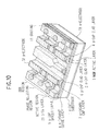
- the integrated optical waveguide device includes four wavelength variable semiconductor lasers, four semiconductor optical modulators and two optical waveguides having four terminals connected with the four modulators to provide four parallel lasing and modulating structures.
- Each of the four wavelength variable semiconductor laser is a three-electrote DBR laser including an active region, a phase adjusting region and a DBR region.
- An active layer 3 is formed only in the active region, while a waveguide layer 10 is formed commonly in the phase adjusting region, the DBR region, the modulator region and the waveguide region.
- the active layer 3 and the waveguide layer 10 are connected with each other at a joint 12.
- the active layer 3 and the waveguide layer 10 are both mesa-etched to be a stripe having a width of approximately 1.5 »m.
- a high resistance InP layer 13 is formed to be buried between adjacent two of the four parallel structures for confinement of a current flowing within each of the structures and isolation therebetween.
- a grating 11 is formed only within the DBR region on the surface of an n-InP substrate 1. Then, an n-InGaAsP guide layer 8, an active layer 3, a p-InP clad layer 4 are deposited in this order. Then, the p-InP clad layer 4 and the InGaAsP active layer 3 in all of the regions, except for the active region, are removed using an SiO2 layer as a mask. Then, the InGaAsP waveguide layer 10 and a p-InP clad layer 4 are grown selectively on the predetermined region.
- the fabricated surface of the n-InP substrate 1, except for the areas forming the elements, are mesa-etched using an SiO2 layer as a mask. Then, an Fe-doped high resistance InP layer 13 and an n-InP layer 5 are grown to be buried. Then, after removing the SiO2 layer, a p-InP layer 6 and a p+-InGaAs cap layer 7 are grown. Then, grooves for insulation are formed between the laser and waveguide regions, and between the adjacent semiconductor lasers. Then, an SiO2 layer 21 is deposited on the entire fabricated surface of the substrate 1.
- p-electrodes 32 are formed to connect the waveguide areas thereof through the openings, while an n-electrodes 33 is formed on the back surface of the n-InP substrate 1.
- MOVPE metalorganic vapor phase epitaxy
- a thin film 21 for selective growth is formed on (100) surface of a semiconductor substrate 1. Then, the thin film 21 is selectively removed to be stripes having side walls 21a parallel to [0 1 1] or [011] direction. Then, a DH structure consisting of a first clad layer 2, an active layer 3 and a second clad layer 4 are formed by MOVPE, as shown in Fig. 4B.
- the DH structure has facets of (111)A surface in [0 1 1] direction and (111)B surface in [011] direction. Additionally, all of the layers composing the DH structure have very flat top surfaces of (100).
- the mixed crystal compositions of the layers are uniform within each surface so far as the stripe width of the thin film 21 is not too large, so that such a layer thus formed can be used as an active layer or a waveguide layer.
- each of the layers has facets of (111), so that the width of the layers can be controlled precisely so far as patterning of an SiO2 layer as a mask is carried out precisely.
- a p-InP clad layer and a p+-InGaAs cap layer are formed by selective growth, and the Method does not include etching of semiconductor layers which causes several troubles, though it includes patterning of dielectric thin films such as an SiO2 layer and selective growth. Therefore, optical semiconductor devices are fabricated from a large size semiconductor wafer by a batch growth process having superior performance such as uniformity or reproducibility due to selective growth of an active layer.
- Fig. 5 shows the relation between SiO2 stripe width and a growth rate in case of InP and InGaAs
- Fig. 6 shows the relation between SiO2 stripe width and composition ratio of In in the mixed crystal of In x Ga 1-x As and In x Ga 1-x As 0.6 P 0.4 in which a light having a wavelength of 1.3 »m is emitted.
- the growth rate of the semiconductor layer becomes large as the width of the SiO2 stripe becomes large, because the growth source materials which are diffused in lateral direction along the SiO2 layer to reach the semiconductor surface becomes large in amount as the width thereof becomes large.
- the In ratio in the composition of the mixed crystal becomes large as the width thereof becomes large, because the source material of In diffuses in lateral direction easier than that of Ga.
- the thickness of the well becomes large and the lattice distortion (compressive stress) is applied to the well so that the amount of In in the composition of the mixed crystal composing the well increases by widening the SiO2 stripe. Consequently, the transition energy of the quantum well structure becomes small.
- Fig. 7 shows the relation between SiO2 stripe width and emission wavelength of the selectively grown layer in case of multi-quantum well (MQW) structure including In x Ga 1-x As well and In x Ga 1-x As y P 1-y barrier selectively grown.
- the wavelength becomes long as the width of the SiO2 stripe becomes large. In practice, the wavelengths become approximately 1.4 »m and 1.55 »m when the widths are approximately 4 »m and 10 »m, respectively. Therefore, a semiconductor laser emitting a light having a wavelength of 1.55 »m and a waveguide layer transmitting a light having a wavelength of 1.3 »m can be fabricated simultaneously by the same process by determining the widths of the semiconductor laser and the waveguide layer so as to have a predetermined ratio. In other words, a laser oscillating region in the direction parallel to a waveguide and a waveguide region which is transparent against the light can be fabricated by use of crystal growth.
- MQW multi-quantum well
- an SiO2 layer 21 having a thickness of approximately 0,2 »m (2000 ⁇ ) is deposited on (100) surface of an n-InP substrate 1 by chemical vapor deposition (CVD). Then, the SiO2 layer 21 is patterned by photolithography to form two stripes each having a width of 10 »m with an interval of 1.8 »m, as shown in Fig. 8A.
- the thicknesses of the layers shown above are measured at the area between the two SiO2 stripes 21 corresponding to an active region, and the thicknesses thereof are uniform in the active region. Then, the SiO2 layers 21 are removed as wide as 10 »m setting the removing center line at the center line of the active region, as shown in Fig. 8C. Then, a p-InP clad layer 6 having a thickness of 1.5 »m and a carrier concentration of 5 ⁇ 1017 cm ⁇ 3 and a p+-InGaAs cap layer 7 having a thickness of 0.3 »m and a carrier concentration of 1 ⁇ 1019 cm ⁇ 3 are selectively grown in this order in the area between the two remaining SiO2 layers 21.
- a second SiO2 layer 22 is formed throughout the fabricated surface of the n-InP substrate 1, and the second SiO2 layer 22 is etched to have a stripe opening above the active region, as shown in Fig. 8E.
- a p-electrode 32 is formed to connect with the active region through the stripe opening, while an n-electrode 33 is formed on the back surface of the n-InP substrate 1, as shown in Fig. 8F.
- a bulk layer of InGaAsP is used for the active layer, however, an MQW structure may be used instead of the bulk layer to improve the characteristics thereof considerably.
- a p-type substrate may be used instead of an n-type substrate used in the embodiment. In this case, the conduction type of each of layers becomes reversed one as compared with that in the embodiment.
- a grating (diffraction lattice) 11 in the direction of [011] is formed only within a laser region on (100) surface of an n-InP substrate 1, as shown in Fig. 9A.
- an n-InCaAsP guide layer 8 having the composition corresponding to a wavelength of 1.3 »m, a carrier concentration of 1 ⁇ 1018 cm ⁇ 3 and a thickness of 0.1 »m (1000 ⁇ ) and an n-InP spacer layer 9 having a carrier concentration of 1 ⁇ 1018 cm ⁇ 3 and a thickness of 0.05 »m (500 ⁇ ) are grown in this order on the n-InP substrate 1, as shown in Fig. 9B.
- an SiO2 layer 21 is formed on the n-InP spacer layer 9, and the SiO2 layer 21 is patterned to be a pair of stripes parallel each other with an interval of 2 »m and each having a width of 10 »m in the laser region and 6 »m in the modulator region, as shown in Fig. 9C.
- Bach of the stripes has a transition width of 20 »m.
- an n-InP clad layer 2 having a carrier concentration of 1 ⁇ 1018 cm ⁇ 3 and a thickness of 0.05 »m (500 ⁇ ), an MQW active layer 3, and a p-InP clad layer 4 having a carrier concentration of 5 ⁇ 1017 cm ⁇ 3 and a thickness of 0.05 »m (500 ⁇ ) are the selectively grown in this order with using the stripes of the SiO2 layer 21 as masks to form a waveguide region, as shown in Fig. 9D.
- the MQW active layer 3 has an MQW structure including a well of InGaAs and a barrier of InCaAsP and having a well number of 4.
- the growth conditions of the layers are set so that the well and the barrier are both lattice matched with the n-InP substrate 1 in the active region and thicknesses of the well and the barrier become respectively 7.5 nm (75 ⁇ ) and 15 nm (150 ⁇ ).
- the emission wavelength becomes 1.56 »m in the active region and 1.48 »m in the modulator region.
- the SiO2 layers 21 are removed on both sides of the waveguide region to have stripe shaped openings having width of 2 »m, as shown in Fig. 9E.
- a p-InP clad layer 6 having a carrier concentration of 5 ⁇ 1017 cm ⁇ 3 and a thickness of 1.5 »m and a p+-InGaAs cap layer 7 having a thickness of 0.3 »m and a carrier concentration of 1 ⁇ 1019 cm ⁇ 3 are selectively grown in this order, as shown in Fig. 9F.
- an SiO2 layer is formed all over the fabricated surface of the n-InP substrate 1, and the SiO2 layer is removed to form a stripe shaped opening having a width of 20 »m above the laser region and the modulator region.
- the p+-InGaAs cap layer 7 is removed in the area between the laser and modulator regions by etching to make isolation therebetween.
- pad-shaped p-electrodes are formed on the fabricated surface to connect with the laser and modulator regions through the openings, while an n-electrode is formed on the back surface of the n-InP substrate 1.
- the laser region length having a cleavage surface is 500 »m and the modulator region length is 200 »m.
- the oscillation threshold current is 20 mA and the maximum CW optical output from the modulator is 30 mW.
- the oscillation wavelength is 1.55 »m, and the extinction ratio is 20 dB when the modulator region is applied with a voltage of -3V.
- the coupling efficiency estimated by the extinction characteristic was found to be as large as 98 %.
- the isolation resistance between the laser and modulator regions is 50 k ⁇ . Any of 20 samples in random selected from the fabricated devices has the extinction ratio not snaller than 15 dB on condition of being applied with -5V.
- a grating 11 is formed only within a DBR region on an n-InP substrate 1. Then, an n-InCaAsP guide layer 8 having a composition corresponding to a wavelength of 1.3 »m, a carrier concentration of 1 ⁇ 1018 cm ⁇ 3 and a thickness of approximately 0.1 »m (1000 ⁇ ), and an n-InP spacer layer 9 having a carrier concentration of 1 ⁇ 1018 cm ⁇ 3 and a thickness of approximately 0.05 »m (500 ⁇ ) are grown in this order.
- an SiO2 layer formed on the n-InP spacer layer 9, and the SiO2 layer is patterned to be a pair of stripes parallel each other with an interval of 2 »m and each having a width of 10 »m in the active region and 4 »m in both the phase adjusting region and the DBR region.
- Each of the stripes has a transition width of 20 »m.
- an n-InP clad layer 2 having a carrier concentration of 1 ⁇ 1018 cm ⁇ 3 and a thickness of 0.05 »m (500 ⁇ ), an MQW active layer 3, and a p-InP clad layer 4 having a carrier concentration of 5 ⁇ 1017 cm ⁇ 3 and a thickness of 0.05 »m (500 ⁇ ) are selectively grown in this order using the stripes of the SiO2 layer as masks to form a waveguide region.
- the MQW active layer 3 has an MQW structure including a well of InGaAs and a barrier of InGaAsP and having a well number of 4.
- the growth conditions of the layers are set so that the well and the barrier are both lattice matched with the n-InP substrate 1 in the active region and thicknesses of the well and the barrier become respectively 7.5 nm (75 ⁇ ) and 15 nm (150 ⁇ ).
- the emission wavelength becomes 1.56 »m in the active region and approximately 1.4 »m in both the phase adjusting region and the DBR region.
- the SiO2 layers are removed in both sides of the waveguide region to have stripe shaped openings having a width of 2 »m.
- a p-InP clad layer 6 having a carrier concentration of 5 ⁇ 1017 cm ⁇ 3 and a thickness of 1.5 »m and a p+-InGaAs cap layer 7 having a thickness of 0.3 »m and a carrier concentration of 1 ⁇ 1019 cm ⁇ 3 are selectively grown in this order.
- an SiO2 layer is formed all over the fabricated surface of the n-InP substrate 1, and the SiO2 layer is removed to form a stripe shaped opening having a width of 20 »m.
- the p+-InGaAs cap layer 7 is removed in the area between the regions by etching to make isolation therebetween.
- pad-shaped p-electrodes 32 are formed on the fabricated surface, while an n-electrode 33 is formed on the back surface of the n-InP substrate 1.
- the active region length having a cleavage surface is 500 »m
- the phase adjusting region length is 150 »m
- the DBR region length is 300 »m.
- the distance between the waveguides is 600 »m
- an irradiation facet of the DBR region is coated with an anti-reflection film.
- the oscillation threshold current is 18 mA.
- the oscillation wavelength of the 4 channels is 1.553 »m ⁇ 0.003 »m when a current is injected into only the active region. It was confirmed that the DBR semiconductor array operates in a single mode until the optical output becomes as large as 30 mW. It is possible to obtain a wide range of the wavelength variable not narrower than 5 nm in each channel with keeping the optical output to be 5 mW by injecting a current to the phase adjusting and DBR regions.
- the current confinement structure may be replaced by one using proton implantation method instead of the selective growth.
Landscapes
- Physics & Mathematics (AREA)
- Electromagnetism (AREA)
- Optics & Photonics (AREA)
- Engineering & Computer Science (AREA)
- Condensed Matter Physics & Semiconductors (AREA)
- General Physics & Mathematics (AREA)
- Nanotechnology (AREA)
- Chemical & Material Sciences (AREA)
- Computer Hardware Design (AREA)
- Microelectronics & Electronic Packaging (AREA)
- Power Engineering (AREA)
- Plasma & Fusion (AREA)
- Life Sciences & Earth Sciences (AREA)
- Biophysics (AREA)
- Manufacturing & Machinery (AREA)
- Crystallography & Structural Chemistry (AREA)
- Geometry (AREA)
- Semiconductor Lasers (AREA)
Claims (6)
- Procédé de fabrication d'un dispositif optique à semi-conducteurs, comprenant les étapes de :a) formation d'une couche diélectrique sur un substrat semi-conducteur,b) mise en forme de ladite couche diélectrique pour qu'elle ait au moins deux bandes parallèles entre elles, avec un intervalle prédéterminé,c) croissance par épitaxie organométallique en phase vapeur d'un cristal sélectivement sur ledit substrat semi-conducteur en utilisant lesdites bandes de ladite couche diélectrique comme masque, etd) formation d'une structure multicouche qui doit avoir une largeur prédéterminée déterminée par la largeur dudit cristal qu'on a fait croître entre lesdites deux bandes,caractérisé par :
e) gravure desdites bandes de ladite couche diélectrique pour changer la largeur pour une autre croissance sélective d'un cristal. - Procédé selon la revendication 1, dans lequel une couche de SiO₂ est formée dans l'étape a).
- Procédé selon la revendication 1 ou 2, dans lequel une structure multicouche incluant une couche sélectionnée dans un groupe incluant une couche active et une couche de guide d'onde, est formée dans l'étape d).
- Procédé selon la revendication 1, 2 ou 3, comprenant en outre l'étape de gravure desdites deux bandes de ladite couche diélectrique en des parties en face l'une de l'autre pour exposer une surface dudit substrat semi-conducteur après ladite étape de croissance d'un cristal.
- Procédé selon l'une quelconque des revendications 1 à 4, comprenant l'étape de croissance d'un cristal sélectivement pour qu'il soit une couche de revêtement sur ledit substrat semi-conducteur incluant au moins la zone entre lesdites deux bandes de ladite couche diélectrique après l'étape de gravure desdites deux bandes de ladite couche diélectrique.
- Procédé selon l'une quelconque des revendications 1 à 5, dans lequel on fait croître sélectivement des composés III-V dans l'étape c).
Priority Applications (1)
| Application Number | Priority Date | Filing Date | Title |
|---|---|---|---|
| EP94118307A EP0643461B1 (fr) | 1990-08-24 | 1991-08-26 | Méthode pour la fabrication d'un dispositif optique à semi-conducteur |
Applications Claiming Priority (4)
| Application Number | Priority Date | Filing Date | Title |
|---|---|---|---|
| JP222928/90 | 1990-08-24 | ||
| JP2222928A JPH0750815B2 (ja) | 1990-08-24 | 1990-08-24 | 半導体光集積素子の製造方法 |
| JP3067498A JP2701569B2 (ja) | 1991-04-01 | 1991-04-01 | 光半導体素子の製造方法 |
| JP67498/91 | 1991-04-01 |
Related Child Applications (1)
| Application Number | Title | Priority Date | Filing Date |
|---|---|---|---|
| EP94118307.1 Division-Into | 1991-08-26 |
Publications (3)
| Publication Number | Publication Date |
|---|---|
| EP0472221A2 EP0472221A2 (fr) | 1992-02-26 |
| EP0472221A3 EP0472221A3 (en) | 1992-05-13 |
| EP0472221B1 true EP0472221B1 (fr) | 1995-12-20 |
Family
ID=26408721
Family Applications (2)
| Application Number | Title | Priority Date | Filing Date |
|---|---|---|---|
| EP91114272A Expired - Lifetime EP0472221B1 (fr) | 1990-08-24 | 1991-08-26 | Méthode pour la fabrication d'un dispositif optique à semi-conducteur |
| EP94118307A Expired - Lifetime EP0643461B1 (fr) | 1990-08-24 | 1991-08-26 | Méthode pour la fabrication d'un dispositif optique à semi-conducteur |
Family Applications After (1)
| Application Number | Title | Priority Date | Filing Date |
|---|---|---|---|
| EP94118307A Expired - Lifetime EP0643461B1 (fr) | 1990-08-24 | 1991-08-26 | Méthode pour la fabrication d'un dispositif optique à semi-conducteur |
Country Status (3)
| Country | Link |
|---|---|
| US (1) | US5250462A (fr) |
| EP (2) | EP0472221B1 (fr) |
| DE (2) | DE69128097T2 (fr) |
Families Citing this family (53)
| Publication number | Priority date | Publication date | Assignee | Title |
|---|---|---|---|---|
| EP0503729A3 (en) * | 1991-03-15 | 1992-12-02 | N.V. Philips' Gloeilampenfabrieken | Optoelectronic semiconductor device and method of manufacturing such a device |
| JP2876839B2 (ja) * | 1991-07-31 | 1999-03-31 | 日本電気株式会社 | 光半導体素子の製造方法 |
| EP0558089B1 (fr) * | 1992-02-28 | 2002-06-05 | Hitachi, Ltd. | Dispositif optique, intégré à semi-conducteur et méthode de fabrication, et récepteur de lumière utilisant ce dispositif |
| JP2950028B2 (ja) * | 1992-07-23 | 1999-09-20 | 日本電気株式会社 | 光半導体素子の製造方法 |
| US5360763A (en) * | 1992-09-07 | 1994-11-01 | Nec Corporation | Method for fabricating an optical semiconductor device |
| JP2815769B2 (ja) * | 1992-12-15 | 1998-10-27 | 三菱電機株式会社 | 半導体レーザの製造方法 |
| JPH0770791B2 (ja) * | 1992-12-22 | 1995-07-31 | 日本電気株式会社 | 半導体レーザ及びその製造方法 |
| EP0606093B1 (fr) * | 1993-01-07 | 1997-12-17 | Nec Corporation | Circuit semi-conducteur optique, intégré, et méthode de fabrication |
| JPH0738204A (ja) * | 1993-07-20 | 1995-02-07 | Mitsubishi Electric Corp | 半導体光デバイス及びその製造方法 |
| JPH07176827A (ja) * | 1993-08-20 | 1995-07-14 | Mitsubishi Electric Corp | 変調器付半導体レーザ装置の製造方法 |
| DE69414208T2 (de) * | 1993-08-31 | 1999-03-25 | Fujitsu Ltd | Optischer Halbleitervorrichtung und Herstellungsverfahren |
| US5543957A (en) * | 1993-12-20 | 1996-08-06 | Nec Corporation | Optical modulator and method of producing the same |
| JP3098371B2 (ja) * | 1993-12-27 | 2000-10-16 | 日本電気株式会社 | 半導体結晶成長方法 |
| JP2682421B2 (ja) | 1993-12-28 | 1997-11-26 | 日本電気株式会社 | 半導体光集積回路の製造方法 |
| JP3510305B2 (ja) * | 1994-02-22 | 2004-03-29 | 三菱電機株式会社 | 半導体レーザの製造方法,及び半導体レーザ |
| JP2982619B2 (ja) * | 1994-06-29 | 1999-11-29 | 日本電気株式会社 | 半導体光導波路集積型受光素子 |
| US5656539A (en) * | 1994-07-25 | 1997-08-12 | Mitsubishi Denki Kabushiki Kaisha | Method of fabricating a semiconductor laser |
| US5610095A (en) * | 1994-08-31 | 1997-03-11 | Lucent Technologies Inc. | Monolithically integrated circuits having dielectrically isolated, electrically controlled optical devices and process for fabricating the same |
| EP0704913B1 (fr) * | 1994-09-28 | 1999-09-01 | Nippon Telegraph And Telephone Corporation | Dispositif optique à semi-conducteur et méthode de fabrication |
| JPH08307012A (ja) * | 1995-05-01 | 1996-11-22 | Mitsubishi Electric Corp | 選択成長用マスク,半導体光装置の製造方法,および半導体光装置 |
| FR2737813B1 (fr) * | 1995-08-08 | 1997-10-31 | France Telecom | Composant laser pour la generation d'ondes millimetriques |
| JP3553222B2 (ja) * | 1995-09-20 | 2004-08-11 | 三菱電機株式会社 | 光変調器モジュール |
| DE19619533A1 (de) * | 1996-05-15 | 1997-11-20 | Sel Alcatel Ag | Monolithisch integriertes optisches Halbleiterbauelement |
| DE19652529A1 (de) * | 1996-12-17 | 1998-06-18 | Siemens Ag | Optoelektronisches Bauelement mit MQW-Strukturen |
| DE19653094A1 (de) * | 1996-12-20 | 1998-06-25 | Alsthom Cge Alcatel | Photonisches Bauelement mit elektrischen Leiterbahnen |
| JP2924852B2 (ja) * | 1997-05-16 | 1999-07-26 | 日本電気株式会社 | 光半導体装置及びその製造方法 |
| DE19838810B4 (de) * | 1998-08-26 | 2006-02-09 | Osram Opto Semiconductors Gmbh | Verfahren zum Herstellen einer Mehrzahl von Ga(In,Al)N-Leuchtdiodenchips |
| JP3024611B2 (ja) | 1997-10-20 | 2000-03-21 | 日本電気株式会社 | 半導体レーザおよびその製造方法 |
| US7408249B2 (en) * | 1998-02-06 | 2008-08-05 | Tessera Technologies Hungary Kft. | Packaged integrated circuits and methods of producing thereof |
| IL123207A0 (en) | 1998-02-06 | 1998-09-24 | Shellcase Ltd | Integrated circuit device |
| GB9815573D0 (en) * | 1998-07-18 | 1998-09-16 | Secr Defence | Electro-optic semiconductor devices and methods for making the same |
| FR2786887B1 (fr) * | 1998-12-08 | 2001-01-26 | Cit Alcatel | Modulateur de phase a semi-conducteur |
| SE515915C2 (sv) * | 1998-12-18 | 2001-10-29 | Ericsson Telefon Ab L M | Metod och integrerad krets för våglängdkompensering vid halvledartillverkning |
| JP3329764B2 (ja) * | 1999-05-13 | 2002-09-30 | 日本電気株式会社 | 半導体レーザー及び半導体光増幅器 |
| JP2001044566A (ja) * | 1999-07-28 | 2001-02-16 | Nec Corp | 半導体レーザおよびその製造方法 |
| US6856007B2 (en) | 2001-08-28 | 2005-02-15 | Tessera, Inc. | High-frequency chip packages |
| US7058246B2 (en) | 2001-10-09 | 2006-06-06 | Infinera Corporation | Transmitter photonic integrated circuit (TxPIC) chip with enhanced power and yield without on-chip amplification |
| JP3912117B2 (ja) * | 2002-01-17 | 2007-05-09 | ソニー株式会社 | 結晶成長方法、半導体発光素子及びその製造方法 |
| US20040004217A1 (en) * | 2002-03-06 | 2004-01-08 | Vijaysekhar Jayaraman | Semiconductor opto-electronic devices with wafer bonded gratings |
| SE0200750D0 (sv) * | 2002-03-13 | 2002-03-13 | Optillion Ab | Method for manufacturing av photonic device and a photonic device |
| SE0200751D0 (sv) * | 2002-03-13 | 2002-03-13 | Optillion Ab | Method for manufacturing a photonic device and photonic device |
| US6972480B2 (en) * | 2003-06-16 | 2005-12-06 | Shellcase Ltd. | Methods and apparatus for packaging integrated circuit devices |
| JP2007528120A (ja) * | 2003-07-03 | 2007-10-04 | テッセラ テクノロジーズ ハンガリー コルラートルト フェレロェセーギュー タールシャシャーグ | 集積回路装置をパッケージングする方法及び装置 |
| DE10335081A1 (de) | 2003-07-31 | 2005-03-03 | Osram Opto Semiconductors Gmbh | Verfahren zur Herstellung einer Vielzahl von optoelektronischen Halbleiterchips und optoeleketronischer Halbleiterchip |
| DE10335080A1 (de) | 2003-07-31 | 2005-03-03 | Osram Opto Semiconductors Gmbh | Verfahren zur Herstellung einer Vielzahl von optoelektronischen Halbleiterchips und optoelektronischer Halbleiterchip |
| US7129576B2 (en) | 2003-09-26 | 2006-10-31 | Tessera, Inc. | Structure and method of making capped chips including vertical interconnects having stud bumps engaged to surfaces of said caps |
| US8143095B2 (en) | 2005-03-22 | 2012-03-27 | Tessera, Inc. | Sequential fabrication of vertical conductive interconnects in capped chips |
| US7566853B2 (en) * | 2005-08-12 | 2009-07-28 | Tessera, Inc. | Image sensor employing a plurality of photodetector arrays and/or rear-illuminated architecture |
| US7936062B2 (en) | 2006-01-23 | 2011-05-03 | Tessera Technologies Ireland Limited | Wafer level chip packaging |
| US8604605B2 (en) | 2007-01-05 | 2013-12-10 | Invensas Corp. | Microelectronic assembly with multi-layer support structure |
| US8213751B1 (en) * | 2008-11-26 | 2012-07-03 | Optonet Inc. | Electronic-integration compatible photonic integrated circuit and method for fabricating electronic-integration compatible photonic integrated circuit |
| CN106990461B (zh) * | 2016-01-20 | 2020-05-15 | 安徽中科米微电子技术有限公司 | 一种直角顶角硅阶梯光栅及其制造方法 |
| WO2018134950A1 (fr) * | 2017-01-19 | 2018-07-26 | 三菱電機株式会社 | Élément laser à semi-conducteurs et procédé de fabrication d'élément laser à semi-conducteurs |
Family Cites Families (8)
| Publication number | Priority date | Publication date | Assignee | Title |
|---|---|---|---|---|
| JPS61104687A (ja) * | 1984-10-29 | 1986-05-22 | Toshiba Corp | 埋込み型半導体レ−ザの製造方法 |
| JPS62144385A (ja) * | 1985-12-19 | 1987-06-27 | Fujitsu Ltd | 半導体レ−ザ及びその製造方法 |
| JP2743377B2 (ja) * | 1987-05-20 | 1998-04-22 | 日本電気株式会社 | 半導体薄膜の製造方法 |
| JPS6455887A (en) * | 1987-08-26 | 1989-03-02 | Nec Corp | Manufacture of semiconductor laser |
| US4826784A (en) * | 1987-11-13 | 1989-05-02 | Kopin Corporation | Selective OMCVD growth of compound semiconductor materials on silicon substrates |
| JPH069280B2 (ja) * | 1988-06-21 | 1994-02-02 | 松下電器産業株式会社 | 半導体レーザ装置 |
| JPH02237021A (ja) * | 1989-03-09 | 1990-09-19 | Fujitsu Ltd | 半導体装置の製造方法 |
| US5070510A (en) * | 1989-12-12 | 1991-12-03 | Sharp Kabushiki Kaisha | Semiconductor laser device |
-
1991
- 1991-08-26 EP EP91114272A patent/EP0472221B1/fr not_active Expired - Lifetime
- 1991-08-26 EP EP94118307A patent/EP0643461B1/fr not_active Expired - Lifetime
- 1991-08-26 US US07/750,172 patent/US5250462A/en not_active Expired - Lifetime
- 1991-08-26 DE DE69128097T patent/DE69128097T2/de not_active Expired - Lifetime
- 1991-08-26 DE DE69115596T patent/DE69115596T2/de not_active Expired - Lifetime
Also Published As
| Publication number | Publication date |
|---|---|
| DE69115596T2 (de) | 1996-09-19 |
| EP0643461B1 (fr) | 1997-10-29 |
| US5250462A (en) | 1993-10-05 |
| DE69128097D1 (de) | 1997-12-04 |
| EP0643461A2 (fr) | 1995-03-15 |
| EP0472221A2 (fr) | 1992-02-26 |
| EP0472221A3 (en) | 1992-05-13 |
| DE69115596D1 (de) | 1996-02-01 |
| DE69128097T2 (de) | 1998-02-26 |
| EP0643461A3 (fr) | 1996-01-03 |
Similar Documents
| Publication | Publication Date | Title |
|---|---|---|
| EP0472221B1 (fr) | Méthode pour la fabrication d'un dispositif optique à semi-conducteur | |
| US5991322A (en) | Semiconductor optical device | |
| EP0836255B1 (fr) | Réseau laser à diode et méthode de fabrication | |
| US5565693A (en) | Semiconductor optical integrated circuits | |
| US5872022A (en) | Method for etching a semiconductor method for fabricating semiconductor device method for fabricating semiconductor laser and semiconductor laser | |
| Coleman et al. | Progress in InGaAs-GaAs selective-area MOCVD toward photonic integrated circuits | |
| JP3194503B2 (ja) | 化合物半導体装置及びその製造方法 | |
| EP0177221B1 (fr) | Laser à semi-conducteur | |
| EP0680119B1 (fr) | Procédé de fabrication d'un dispositif optique à semi-conducteur | |
| EP0378098B1 (fr) | Dispositif optique à semi-conducteur | |
| JPH07211984A (ja) | 光半導体デバイス及びその製造方法 | |
| JP2701569B2 (ja) | 光半導体素子の製造方法 | |
| EP0527615A1 (fr) | Méthode pour la fabrication d'un laser à semi-conducteur accordable | |
| US5303255A (en) | Distributed feedback semiconductor laser device and a method of producing the same | |
| JP2001156391A (ja) | 光半導体装置およびその製造方法 | |
| US5756373A (en) | Method for fabricating optical semiconductor device | |
| JP2950028B2 (ja) | 光半導体素子の製造方法 | |
| EP1168541B1 (fr) | Laser à mode unique à haute puissance et méthode de fabrication | |
| JP2882335B2 (ja) | 光半導体装置およびその製造方法 | |
| JPH1022579A (ja) | 光導波路構造とこの光導波路構造を用いた半導体レーザ、変調器及び集積型半導体レーザ装置 | |
| JPH06196797A (ja) | 光変調器集積化光源素子およびその製造方法 | |
| US5360763A (en) | Method for fabricating an optical semiconductor device | |
| GB2292011A (en) | Semiconductor optical devices and methods for fabrication | |
| JPH06283802A (ja) | 半導体レーザ装置及びその製造方法 | |
| JP2932690B2 (ja) | 光半導体素子の製造方法 |
Legal Events
| Date | Code | Title | Description |
|---|---|---|---|
| PUAI | Public reference made under article 153(3) epc to a published international application that has entered the european phase |
Free format text: ORIGINAL CODE: 0009012 |
|
| 17P | Request for examination filed |
Effective date: 19910925 |
|
| AK | Designated contracting states |
Kind code of ref document: A2 Designated state(s): DE FR GB NL |
|
| PUAL | Search report despatched |
Free format text: ORIGINAL CODE: 0009013 |
|
| AK | Designated contracting states |
Kind code of ref document: A3 Designated state(s): DE FR GB NL |
|
| 17Q | First examination report despatched |
Effective date: 19931112 |
|
| GRAA | (expected) grant |
Free format text: ORIGINAL CODE: 0009210 |
|
| AK | Designated contracting states |
Kind code of ref document: B1 Designated state(s): DE FR GB NL |
|
| XX | Miscellaneous (additional remarks) |
Free format text: TEILANMELDUNG 94118307.1 EINGEREICHT AM 26/08/91. |
|
| REF | Corresponds to: |
Ref document number: 69115596 Country of ref document: DE Date of ref document: 19960201 |
|
| ET | Fr: translation filed | ||
| PLBE | No opposition filed within time limit |
Free format text: ORIGINAL CODE: 0009261 |
|
| STAA | Information on the status of an ep patent application or granted ep patent |
Free format text: STATUS: NO OPPOSITION FILED WITHIN TIME LIMIT |
|
| 26N | No opposition filed | ||
| REG | Reference to a national code |
Ref country code: GB Ref legal event code: IF02 |
|
| PGFP | Annual fee paid to national office [announced via postgrant information from national office to epo] |
Ref country code: FR Payment date: 20090814 Year of fee payment: 19 |
|
| PGFP | Annual fee paid to national office [announced via postgrant information from national office to epo] |
Ref country code: NL Payment date: 20090816 Year of fee payment: 19 Ref country code: DE Payment date: 20090821 Year of fee payment: 19 Ref country code: GB Payment date: 20090826 Year of fee payment: 19 |
|
| REG | Reference to a national code |
Ref country code: NL Ref legal event code: V1 Effective date: 20110301 |
|
| GBPC | Gb: european patent ceased through non-payment of renewal fee |
Effective date: 20100826 |
|
| REG | Reference to a national code |
Ref country code: FR Ref legal event code: ST Effective date: 20110502 |
|
| PG25 | Lapsed in a contracting state [announced via postgrant information from national office to epo] |
Ref country code: NL Free format text: LAPSE BECAUSE OF NON-PAYMENT OF DUE FEES Effective date: 20110301 |
|
| REG | Reference to a national code |
Ref country code: DE Ref legal event code: R119 Ref document number: 69115596 Country of ref document: DE Effective date: 20110301 |
|
| PG25 | Lapsed in a contracting state [announced via postgrant information from national office to epo] |
Ref country code: FR Free format text: LAPSE BECAUSE OF NON-PAYMENT OF DUE FEES Effective date: 20100831 Ref country code: DE Free format text: LAPSE BECAUSE OF NON-PAYMENT OF DUE FEES Effective date: 20110301 |
|
| PG25 | Lapsed in a contracting state [announced via postgrant information from national office to epo] |
Ref country code: GB Free format text: LAPSE BECAUSE OF NON-PAYMENT OF DUE FEES Effective date: 20100826 |