EP0471109A1 - Verfahren zur Herstellung gerillter Substrate und Multi-Schicht-Struktur - Google Patents
Verfahren zur Herstellung gerillter Substrate und Multi-Schicht-Struktur Download PDFInfo
- Publication number
- EP0471109A1 EP0471109A1 EP90115758A EP90115758A EP0471109A1 EP 0471109 A1 EP0471109 A1 EP 0471109A1 EP 90115758 A EP90115758 A EP 90115758A EP 90115758 A EP90115758 A EP 90115758A EP 0471109 A1 EP0471109 A1 EP 0471109A1
- Authority
- EP
- European Patent Office
- Prior art keywords
- layer
- structured
- accordance
- substrate
- grooves
- Prior art date
- Legal status (The legal status is an assumption and is not a legal conclusion. Google has not performed a legal analysis and makes no representation as to the accuracy of the status listed.)
- Granted
Links
- 239000000758 substrate Substances 0.000 title claims abstract description 51
- 238000004519 manufacturing process Methods 0.000 title claims description 10
- 238000000034 method Methods 0.000 claims abstract description 30
- 230000003287 optical effect Effects 0.000 claims abstract description 22
- 150000001875 compounds Chemical class 0.000 claims abstract description 20
- VYPSYNLAJGMNEJ-UHFFFAOYSA-N Silicium dioxide Chemical compound O=[Si]=O VYPSYNLAJGMNEJ-UHFFFAOYSA-N 0.000 claims abstract description 18
- 239000000463 material Substances 0.000 claims abstract description 18
- 238000002161 passivation Methods 0.000 claims abstract description 10
- 238000007669 thermal treatment Methods 0.000 claims abstract description 10
- GWEVSGVZZGPLCZ-UHFFFAOYSA-N Titan oxide Chemical compound O=[Ti]=O GWEVSGVZZGPLCZ-UHFFFAOYSA-N 0.000 claims abstract description 9
- 235000012239 silicon dioxide Nutrition 0.000 claims abstract description 8
- 239000000377 silicon dioxide Substances 0.000 claims abstract description 8
- 229920000642 polymer Polymers 0.000 claims abstract description 7
- 238000004528 spin coating Methods 0.000 claims abstract description 6
- 229910052681 coesite Inorganic materials 0.000 claims abstract description 5
- 229910052906 cristobalite Inorganic materials 0.000 claims abstract description 5
- 229910052682 stishovite Inorganic materials 0.000 claims abstract description 5
- 229910052905 tridymite Inorganic materials 0.000 claims abstract description 5
- MRELNEQAGSRDBK-UHFFFAOYSA-N lanthanum oxide Inorganic materials [O-2].[O-2].[O-2].[La+3].[La+3] MRELNEQAGSRDBK-UHFFFAOYSA-N 0.000 claims abstract description 4
- HTUMBQDCCIXGCV-UHFFFAOYSA-N lead oxide Chemical compound [O-2].[Pb+2] HTUMBQDCCIXGCV-UHFFFAOYSA-N 0.000 claims abstract description 4
- YEXPOXQUZXUXJW-UHFFFAOYSA-N lead(II) oxide Inorganic materials [Pb]=O YEXPOXQUZXUXJW-UHFFFAOYSA-N 0.000 claims abstract description 4
- KTUFCUMIWABKDW-UHFFFAOYSA-N oxo(oxolanthaniooxy)lanthanum Chemical compound O=[La]O[La]=O KTUFCUMIWABKDW-UHFFFAOYSA-N 0.000 claims abstract description 4
- 150000004760 silicates Chemical class 0.000 claims abstract description 3
- 230000008569 process Effects 0.000 claims description 18
- LYCAIKOWRPUZTN-UHFFFAOYSA-N Ethylene glycol Chemical compound OCCO LYCAIKOWRPUZTN-UHFFFAOYSA-N 0.000 claims description 14
- 239000000203 mixture Substances 0.000 claims description 4
- 238000003860 storage Methods 0.000 claims description 4
- OKTJSMMVPCPJKN-UHFFFAOYSA-N Carbon Chemical compound [C] OKTJSMMVPCPJKN-UHFFFAOYSA-N 0.000 claims description 3
- 229910052799 carbon Inorganic materials 0.000 claims description 3
- 229910052581 Si3N4 Inorganic materials 0.000 claims description 2
- -1 siloxan Chemical class 0.000 claims description 2
- MCMNRKCIXSYSNV-UHFFFAOYSA-N Zirconium dioxide Chemical compound O=[Zr]=O MCMNRKCIXSYSNV-UHFFFAOYSA-N 0.000 claims 2
- 229910017083 AlN Inorganic materials 0.000 claims 1
- PIGFYZPCRLYGLF-UHFFFAOYSA-N Aluminum nitride Chemical compound [Al]#N PIGFYZPCRLYGLF-UHFFFAOYSA-N 0.000 claims 1
- 229910004160 TaO2 Inorganic materials 0.000 claims 1
- 229910052782 aluminium Inorganic materials 0.000 claims 1
- PNEYBMLMFCGWSK-UHFFFAOYSA-N aluminium oxide Inorganic materials [O-2].[O-2].[O-2].[Al+3].[Al+3] PNEYBMLMFCGWSK-UHFFFAOYSA-N 0.000 claims 1
- 229910052804 chromium Inorganic materials 0.000 claims 1
- 229910052593 corundum Inorganic materials 0.000 claims 1
- NQKXFODBPINZFK-UHFFFAOYSA-N dioxotantalum Chemical compound O=[Ta]=O NQKXFODBPINZFK-UHFFFAOYSA-N 0.000 claims 1
- 229910052737 gold Inorganic materials 0.000 claims 1
- 229910052761 rare earth metal Inorganic materials 0.000 claims 1
- 229910052709 silver Inorganic materials 0.000 claims 1
- 230000007704 transition Effects 0.000 claims 1
- 229910001845 yogo sapphire Inorganic materials 0.000 claims 1
- KPUWHANPEXNPJT-UHFFFAOYSA-N disiloxane Chemical class [SiH3]O[SiH3] KPUWHANPEXNPJT-UHFFFAOYSA-N 0.000 abstract description 3
- 239000010410 layer Substances 0.000 description 87
- 239000011521 glass Substances 0.000 description 15
- 238000010586 diagram Methods 0.000 description 8
- 230000004580 weight loss Effects 0.000 description 5
- 238000001035 drying Methods 0.000 description 4
- 239000002904 solvent Substances 0.000 description 4
- 238000005516 engineering process Methods 0.000 description 3
- 230000009467 reduction Effects 0.000 description 3
- PEDCQBHIVMGVHV-UHFFFAOYSA-N Glycerine Chemical compound OCC(O)CO PEDCQBHIVMGVHV-UHFFFAOYSA-N 0.000 description 2
- PXHVJJICTQNCMI-UHFFFAOYSA-N Nickel Chemical compound [Ni] PXHVJJICTQNCMI-UHFFFAOYSA-N 0.000 description 2
- XUIMIQQOPSSXEZ-UHFFFAOYSA-N Silicon Chemical compound [Si] XUIMIQQOPSSXEZ-UHFFFAOYSA-N 0.000 description 2
- 239000011248 coating agent Substances 0.000 description 2
- 238000000576 coating method Methods 0.000 description 2
- 238000011038 discontinuous diafiltration by volume reduction Methods 0.000 description 2
- 230000000694 effects Effects 0.000 description 2
- 230000007246 mechanism Effects 0.000 description 2
- 229910052710 silicon Inorganic materials 0.000 description 2
- 239000010703 silicon Substances 0.000 description 2
- 238000012546 transfer Methods 0.000 description 2
- 230000009466 transformation Effects 0.000 description 2
- RTAQQCXQSZGOHL-UHFFFAOYSA-N Titanium Chemical compound [Ti] RTAQQCXQSZGOHL-UHFFFAOYSA-N 0.000 description 1
- PQZSQOYXZGDGQW-UHFFFAOYSA-N [W].[Pb] Chemical compound [W].[Pb] PQZSQOYXZGDGQW-UHFFFAOYSA-N 0.000 description 1
- 238000004026 adhesive bonding Methods 0.000 description 1
- 239000012790 adhesive layer Substances 0.000 description 1
- 238000007605 air drying Methods 0.000 description 1
- 239000012298 atmosphere Substances 0.000 description 1
- 238000001354 calcination Methods 0.000 description 1
- 238000004140 cleaning Methods 0.000 description 1
- 230000006378 damage Effects 0.000 description 1
- 238000013500 data storage Methods 0.000 description 1
- 230000007423 decrease Effects 0.000 description 1
- 230000001419 dependent effect Effects 0.000 description 1
- 238000011161 development Methods 0.000 description 1
- 230000018109 developmental process Effects 0.000 description 1
- 238000002474 experimental method Methods 0.000 description 1
- 235000011187 glycerol Nutrition 0.000 description 1
- 238000010438 heat treatment Methods 0.000 description 1
- 229910052759 nickel Inorganic materials 0.000 description 1
- 239000012299 nitrogen atmosphere Substances 0.000 description 1
- 238000012536 packaging technology Methods 0.000 description 1
- 239000002245 particle Substances 0.000 description 1
- 238000006068 polycondensation reaction Methods 0.000 description 1
- 238000012545 processing Methods 0.000 description 1
- 239000011241 protective layer Substances 0.000 description 1
- 230000010076 replication Effects 0.000 description 1
- 239000004065 semiconductor Substances 0.000 description 1
- 238000000926 separation method Methods 0.000 description 1
- 125000005372 silanol group Chemical group 0.000 description 1
- HQVNEWCFYHHQES-UHFFFAOYSA-N silicon nitride Chemical compound N12[Si]34N5[Si]62N3[Si]51N64 HQVNEWCFYHHQES-UHFFFAOYSA-N 0.000 description 1
- 229910052814 silicon oxide Inorganic materials 0.000 description 1
- 238000002411 thermogravimetry Methods 0.000 description 1
- 239000002562 thickening agent Substances 0.000 description 1
Images


Classifications
-
- B—PERFORMING OPERATIONS; TRANSPORTING
- B29—WORKING OF PLASTICS; WORKING OF SUBSTANCES IN A PLASTIC STATE IN GENERAL
- B29D—PRODUCING PARTICULAR ARTICLES FROM PLASTICS OR FROM SUBSTANCES IN A PLASTIC STATE
- B29D17/00—Producing carriers of records containing fine grooves or impressions, e.g. disc records for needle playback, cylinder records; Producing record discs from master stencils
- B29D17/005—Producing optically read record carriers, e.g. optical discs
-
- G—PHYSICS
- G11—INFORMATION STORAGE
- G11B—INFORMATION STORAGE BASED ON RELATIVE MOVEMENT BETWEEN RECORD CARRIER AND TRANSDUCER
- G11B7/00—Recording or reproducing by optical means, e.g. recording using a thermal beam of optical radiation by modifying optical properties or the physical structure, reproducing using an optical beam at lower power by sensing optical properties; Record carriers therefor
- G11B7/24—Record carriers characterised by shape, structure or physical properties, or by the selection of the material
- G11B7/241—Record carriers characterised by shape, structure or physical properties, or by the selection of the material characterised by the selection of the material
-
- G—PHYSICS
- G11—INFORMATION STORAGE
- G11B—INFORMATION STORAGE BASED ON RELATIVE MOVEMENT BETWEEN RECORD CARRIER AND TRANSDUCER
- G11B7/00—Recording or reproducing by optical means, e.g. recording using a thermal beam of optical radiation by modifying optical properties or the physical structure, reproducing using an optical beam at lower power by sensing optical properties; Record carriers therefor
- G11B7/24—Record carriers characterised by shape, structure or physical properties, or by the selection of the material
- G11B7/26—Apparatus or processes specially adapted for the manufacture of record carriers
Definitions
- the present invention relates to a process for manufacturing a grooved substrate and to a multilayer structure.
- the grooved substrate and the multilayer structure are especially suitable for optical disks.
- Microstructuring of thin dielectric layers or processes for manufacturing grooved substrates are needed in the whole data processing technology.
- Applications are to be found not only in the semiconductor and packaging technology but also in integrated optics technology, in the storage technology, e.g. for data communications, for magnetic disks and especially for optical disks.
- the high storage density of optical disks is achieved by using beam diameters of approximately 1 ⁇ m.
- the information is recorded at a predetermined position and read out from a predetermined position. Therefore the beam position needs to be accurately controlled by the use of guide addresses or guide signals.
- These typically are microscopic grooves, which in conjunction with a sensing mechanism and a servo system operating upon the optical beam serve to guide the beam in the correct direction during recording and reading operations.
- Various methods for forming the grooves on the optical disk have been proposed.
- PCT/EP88/00479 describes a hot stamping process for forming the tracking grooves directly in the glass surface of an optical disk.
- the glass substrate is heated in excess of the softening point of the glass types used, typically higher than 600°C.
- the temperature of the heated stamp should preferably be lower than the transformation temperature of the glass type used, typically 380 - 450°C.
- the microstructure on the heated stamper deforms the surface of the glass substrate resulting in a corresponding microstructure on the surface of the glass substrate, which, when separated from the stamper and cooled in a controlled manner, gives the desired surface microstructure on the glass substrate.
- Microstructures formed on the surface of the glass substrate using the hot stamping process as described above conform to the microstructure on the stamper across the area of the substrate surface, but, for example, the glass may flow into a deep groove in the stamper to give a shallow protrusion on the substrate surface. Since for reasons of economy and product cost reduction it is desired to re-use the stamper a number of times the hot stamping process needs the selection of appropriate stamping conditions and coating materials for the glass layer to enable a single stamper to be used repeatedly without sticking problems.
- the high temperatures applied to the glass substrate during hot stamping processes e.g.higher than 600°C, may cause the deformation of the glass substrate.
- the method for manufacturing substrates having a large number of fine grooves thereon as described in US-A-4 810 547 comprises applying a solution containing at least one organometal compound and a thickening agent onto a body of substrate to form a film having plasticity, impressing in the surface of the film formed on the substrate with a mold and calcining the film to solidify the same.
- a similar method is claimed in the unexamined Japanese patent application JP 62 102 445.
- grooved substrates and structures When used for optical disks grooved substrates and structures should have a high refractive index and a high signal to noise ratio in addition to the aready mentioned properties. This normally is achieved by producing a multilayer structure on a grooved substrate, as described by Takahashi et al. in "High quality magneto-optical disk", SPIE Vol.695 Optical Mass Data Storage II (1986).
- Another major object of the present invention is to enhance the refractive index and the signal to noise ratio of the grooved substrate especially when used for optical disks.
- a further object of the present invention is to provide a manufacturing process which ensures the re-use of the stamper and which is quite simple and economic.
- a multilayer structure comprising a substrate with plane, unstructured surfaces, a structured glasslike layer provided on one surface of said substrate, wherein said glasslike layer contains grooves in the layer surface not adjacent to said substrate, a dielectric layer disposed on said structured glasslike layer, a magneto-optic layer disposed on said dielectric layer, a reflector layer disposed on said magneto-optic layer and a passivation layer disposed on said reflector layer, wherein said dielectric layer, said magneto-optic layer, said reflector layer and possibly said passivation layer contain the grooves of said structured glasslike layer.
- This multilayer structure and other grooved substrates may be manufactured according to a process comprising the steps of spin coating of a supporting plate with dissolved material, forming a soft layer on said supporting plate, stamping grooves into said soft layer with a stamp, wherein said stamp shows the negative image of the structure to be transmitted to said soft layer thus forming a structured soft layer, hardening of said structured soft layer to transform said structured soft layer into a hard, structured layer, wherein said hardening is accomplished by thermal treatment, wherein said dissolved material contains at least one polymeric organometal compound.
- a supporting plate is spin-coated with dissolved material forming a soft layer on the supporting plate.
- the dissolved material contains controlling compounds and polymeric organometal compounds.
- the controlling compounds control the viscosity of the layer during the following process steps. Especially the spin-on time, the number of revolutions per minute during the spin-on step, the transportation time to the stamp and the time delay until the stamping step is carried out are to be adjusted carefully.
- the controlling compounds comprise ethylene glycol.
- the structured layer is hardened and transformed into a hard structured layer.
- the polymeric organometal compounds comprise polymer siloxane [RxSiOy]n or silsesquioxane, polymeric titanate [TiO2]n and polymer silicates [SiO2]n like phosphosilicates or phosphosiloxane. These materials consist of long molecule chains containing reactive silanolgroups with a high silicon portion.
- the soft structured layer is transformed into a hard, SiO2-like layer.
- thermo gravimetric analysis information about the weight loss of the organometal compounds during the hardening Step may be obtained.
- the weight loss depends on the hardening temperature and the atmosphere.
- ACCUGLASS 204 (trademark of Allied-Signal Inc., Milpitas, CA), containing polymer siloxane as organometal compound, shows a continuous weight loss in the temperature range from 50°C to about 480°C. In air the weight loss is as small as about 13% and in nitrogen atmosphere it is even lower with about 7%. Very low weight losses are shown by ACCUGLASS x11 series with 5% (+/- 1 %).
- the process as claimed leads to less volume shrinkage and thus higher exactness in accepting and keeping the form of the stamp, resulting in grooved substrates with extremely high dimensional stability, sharp edges of the grooves and exact transfer of the stamper image to the substrate, avoiding blisters or cracks in the grooved film.
- the stamping is carried out at room temperature and at low stamping pressure, preferably at about 1 to 6 bar in an isobaric press. These conditions avoid breakage of the stamper plate by foreign particles and the deformation of the microstructure of the stamper.
- the stamp is preferably coated with a thin carbon layer of preferably about 0.4 ⁇ m to prevent it from sticking to the structured soft layer.
- Other coating materials tested like silicon, siliconoxide, siliconnitride, nickel or tungsten lead to a close sticking of the stamp to the structured soft layer.
- the typical adhesion shown by the plane and parallel surfaces of the stamp and the structured layer in intimate contact after the stamping step may be overcome by a special treatment without applying external forces.
- Heating up the stamp to about 130°C assures the uniform detachment of the stamp and the integrity of the grooved structures as well as of the stamp itself.
- small amounts of solvent of the structured layer evaporize forming a sort of gaseous bolster between the coated stamp and the structured layer.
- This detachment mechanism is supported by the different thermal expansion coefficients of the coated stamp and the structured layer.
- a mixture of 1 g ethylene glycole and 30 g Accuglas 204 is spun on the cleaned glass substrate within 10 s at 1500 rpm.
- a stamping pressure of about 6 bar the desired structure is stamped into the spun-on layer with a carbon coated stamp within 3 minutes.
- the structured layer and the stamp adhering to it are heated up to about 130°C.
- the stamp detaches from the grooved substrate more or less automatically, it pops up, without applying external forces.
- the following thermal treatment at about 400°C during about 1 hour transforms the structured soft layer into a hard, transparent layer showing good adhesion to the glass substrate underneath.
- Fig. 1C and Fig. 1D show both a part of the surface of an embodiment.
- the grooves have been stamped after air drying of the spun-on soft layer.
- a prebake and cure step were applied to the soft layer after the stamping step.
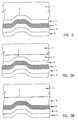
- Fig. 2 is a schematic diagram showing the cross-section of a state of the art grooved structure for optical disks.
- the grooves 2 are provided in the substrate 1 itself and the layers forming the complete structure are disposed on the grooved substrate. These four layers consist of a dielectric layer 3 of about 50 nm, thickness, a magneto-optic layer 4 of about 35 nm thickness, a reflector layer 5 of about 60 nm thickness and a passivation layer 6 of about 100 nm thickness.
- Fig. 3A is a schematic diagram showing the cross-section of one embodiment of the present invention.
- a silicon dioxide layer 7 is disposed on the plane surface of the unstructured substrate 1 and the grooves 2 are provided in the surface of the silicon dioxide layer 7 not adjacent to the unstructured substrate 1.
- the four layers completing the structure are disposed on the grooved silicon dioxide layer 7.
- Four layers are provided with the same specification and in the same sequence as described above in connection with Fig. 2.
- Fig. 3B is the same diagram as in Fig. 3A showing another embodiment in which a dielectric layer 8 is disposed on the plane surface of an unstructured substrate 11.
- the grooves 2 are provided in the surface of the dielectric layer 8 not adjacent to the unstructured substrate 11.
- the dielectric layer 8 contains various combinations of the oxides SiO2, La2O3, PbO and TiO2 and replaces the dielectric layer structure of the embodiment of Fig. 3A consisting of a SiO2-layer and an AlN-layer.
- the refractive index D and the signal-to-noise ratio (SNR) of the structure are enhanced in dependence of the thickness d of the dielectric layer. This is of special importance when the structure is used for optical disks. Receiving these results with only one dielectric layer using the above described composition additionally reduces the complexity of the manufacturing process and the process costs.
- a magneto-optic layer 4 Three layers, a magneto-optic layer 4, a reflector layer 5 and a passivation layer 6 are completing the structure and are disposed on the grooved dielectric layer 8. These three layers have the same specification and are disposed in the same sequence as described above in connection with Fig. 2.
- Fig. 3C shows the cross-section of an embodiment with two multilayer structures attached to each other, e.g.by glueing, allowing at the same time the use of both sides of the structure to read or write information.
- An adhesive layer 9 sandwiched between protective layers 10 links the two multilayer structures.
- 3A and 3B may be manufactured following the process steps of the invention: Spin coating of a supporting plate (1) with dissolved material forming a soft layer (7) on said supporting plate (1), stamping grooves (2) into said soft layer with a stamp, wherein said stamp shows the negative image of the structure to be transmitted to said soft layer (7), thus forming a structured soft layer (7), hardening of said structured soft layer (7) to transform said structured soft layer (7) into a hard, structured layer (7), wherein said hardening is accomplished by thermal treatment, wherein said dissolved material further contains controlling compounds which control the viscosity of said layer during the process steps of spin coating and of stamping grooves, wherein said controlling compounds comprise ethylene glycol.
Landscapes
- Engineering & Computer Science (AREA)
- Manufacturing & Machinery (AREA)
- Mechanical Engineering (AREA)
- Manufacturing Optical Record Carriers (AREA)
- Application Of Or Painting With Fluid Materials (AREA)
- Casting Or Compression Moulding Of Plastics Or The Like (AREA)
- Diffracting Gratings Or Hologram Optical Elements (AREA)
Priority Applications (6)
| Application Number | Priority Date | Filing Date | Title |
|---|---|---|---|
| DE69031802T DE69031802T2 (de) | 1990-08-17 | 1990-08-17 | Verfahren zur Herstellung gerillter Substrate |
| EP90115758A EP0471109B1 (de) | 1990-08-17 | 1990-08-17 | Verfahren zur Herstellung gerillter Substrate |
| JP3201130A JP2758288B2 (ja) | 1990-08-17 | 1991-07-17 | 溝付き基板の製法および多層構造体 |
| CA002049261A CA2049261A1 (en) | 1990-08-17 | 1991-08-15 | Manufacturing process for grooved substrates and multilayer structure |
| KR1019910014143A KR950007444B1 (ko) | 1990-08-17 | 1991-08-16 | 홈이 있는 기판 제조공정, 다층 구조체 및 광학 저장 시스템 |
| US08/311,296 US5498445A (en) | 1990-08-17 | 1994-09-23 | Manufacturing process for grooved substrates and multilayer structure |
Applications Claiming Priority (1)
| Application Number | Priority Date | Filing Date | Title |
|---|---|---|---|
| EP90115758A EP0471109B1 (de) | 1990-08-17 | 1990-08-17 | Verfahren zur Herstellung gerillter Substrate |
Publications (2)
| Publication Number | Publication Date |
|---|---|
| EP0471109A1 true EP0471109A1 (de) | 1992-02-19 |
| EP0471109B1 EP0471109B1 (de) | 1997-12-10 |
Family
ID=8204344
Family Applications (1)
| Application Number | Title | Priority Date | Filing Date |
|---|---|---|---|
| EP90115758A Expired - Lifetime EP0471109B1 (de) | 1990-08-17 | 1990-08-17 | Verfahren zur Herstellung gerillter Substrate |
Country Status (6)
| Country | Link |
|---|---|
| US (1) | US5498445A (de) |
| EP (1) | EP0471109B1 (de) |
| JP (1) | JP2758288B2 (de) |
| KR (1) | KR950007444B1 (de) |
| CA (1) | CA2049261A1 (de) |
| DE (1) | DE69031802T2 (de) |
Families Citing this family (6)
| Publication number | Priority date | Publication date | Assignee | Title |
|---|---|---|---|---|
| TW500701B (en) | 1999-07-07 | 2002-09-01 | Nippon Sheet Glass Co Ltd | Articles having an uneven surface and production process therefor |
| US6479122B2 (en) * | 2000-12-29 | 2002-11-12 | Itrix Corporation | Glass substrate for an optical disk and a manufacturing method thereof |
| US6730617B2 (en) | 2002-04-24 | 2004-05-04 | Ibm | Method of fabricating one or more tiers of an integrated circuit |
| FR2893610B1 (fr) * | 2005-11-23 | 2008-07-18 | Saint Gobain | Procede de structuration de surface d'un produit verrier, produit verrier a surface structuree et utilisations |
| WO2008111312A1 (ja) * | 2007-03-14 | 2008-09-18 | Panasonic Corporation | 多層情報記録媒体の製造方法、並びに、信号転写基板及びその製造方法 |
| US8015970B2 (en) * | 2007-07-26 | 2011-09-13 | 3M Innovative Properties Company | Respirator, welding helmet, or face shield that has low surface energy hard-coat lens |
Citations (1)
| Publication number | Priority date | Publication date | Assignee | Title |
|---|---|---|---|---|
| US4810547A (en) * | 1986-03-26 | 1989-03-07 | Nippon Sheet Glass Co., Ltd. | Substrate with fine grooves and method for manufacturing the same |
Family Cites Families (11)
| Publication number | Priority date | Publication date | Assignee | Title |
|---|---|---|---|---|
| JPS6070537A (ja) * | 1983-09-27 | 1985-04-22 | Ricoh Co Ltd | 光情報担体の製造法 |
| EP0181941B1 (de) * | 1984-05-07 | 1990-01-24 | TDK Corporation | Optisches speichermedium |
| JPS61131251A (ja) * | 1984-11-29 | 1986-06-18 | Matsushita Electric Ind Co Ltd | 光デイスク基板 |
| US4801499A (en) * | 1985-01-24 | 1989-01-31 | Seiko Epson Corporation | Optical recording medium |
| KR920010028B1 (ko) * | 1986-04-10 | 1992-11-13 | 세이꼬 엡슨 가부시끼가이샤 | 광기록 매체 |
| US5156941A (en) * | 1986-06-17 | 1992-10-20 | Kyodo Printing Co., Ltd. | Method of producing an optical or magneto-optical recording card and transfer type optical or magneto-optical recording medium |
| CA1324213C (en) * | 1987-06-26 | 1993-11-09 | Yoshimitsu Kobayashi | Magnetooptical recording media |
| JP2720435B2 (ja) * | 1987-07-08 | 1998-03-04 | 日本板硝子株式会社 | 溝つき基板 |
| JPH01204243A (ja) * | 1988-02-09 | 1989-08-16 | Mitsubishi Kasei Corp | 光磁気記録媒体 |
| JP2538972B2 (ja) * | 1988-03-11 | 1996-10-02 | 株式会社東芝 | 光ディスク基板の製造方法 |
| US5188863A (en) * | 1989-06-30 | 1993-02-23 | E. I. Du Pont De Nemours And Company | Direct effect master/stamper for optical recording |
-
1990
- 1990-08-17 DE DE69031802T patent/DE69031802T2/de not_active Expired - Fee Related
- 1990-08-17 EP EP90115758A patent/EP0471109B1/de not_active Expired - Lifetime
-
1991
- 1991-07-17 JP JP3201130A patent/JP2758288B2/ja not_active Expired - Lifetime
- 1991-08-15 CA CA002049261A patent/CA2049261A1/en not_active Abandoned
- 1991-08-16 KR KR1019910014143A patent/KR950007444B1/ko not_active IP Right Cessation
-
1994
- 1994-09-23 US US08/311,296 patent/US5498445A/en not_active Expired - Fee Related
Patent Citations (1)
| Publication number | Priority date | Publication date | Assignee | Title |
|---|---|---|---|---|
| US4810547A (en) * | 1986-03-26 | 1989-03-07 | Nippon Sheet Glass Co., Ltd. | Substrate with fine grooves and method for manufacturing the same |
Also Published As
| Publication number | Publication date |
|---|---|
| KR920005083A (ko) | 1992-03-28 |
| KR950007444B1 (ko) | 1995-07-11 |
| DE69031802T2 (de) | 1998-06-25 |
| US5498445A (en) | 1996-03-12 |
| EP0471109B1 (de) | 1997-12-10 |
| DE69031802D1 (de) | 1998-01-22 |
| CA2049261A1 (en) | 1992-02-18 |
| JP2758288B2 (ja) | 1998-05-28 |
| JPH04232629A (ja) | 1992-08-20 |
Similar Documents
| Publication | Publication Date | Title |
|---|---|---|
| US4619804A (en) | Fabricating optical record media | |
| CA1066411A (en) | Video disc and method of making the same | |
| KR960032325A (ko) | 광학기록매체 및 그 제조방법 | |
| KR100284728B1 (ko) | 광 디스크 제조방법 및 이 제조방법에 의한 광 디스크 | |
| EP0471109B1 (de) | Verfahren zur Herstellung gerillter Substrate | |
| EP0335172B1 (de) | Giessform zum Giessen eines Laminats für Informationssträger, Verfahren zum Vorbereiten des Laminats für den Informationsträger und Verfahren zum Vorbereiten des Informationsträgers durch Verwendung des Laminats | |
| EP0240752B1 (de) | Löschbare optische Platte mit optisch transparentem Substrat | |
| JPH04372741A (ja) | 両面タイプの2p基板の製造方法 | |
| US6150000A (en) | Magneto-optical disk and superdensity disk employing integral substrate, and method for manufacturing the same | |
| JP2693950B2 (ja) | 光学式デイスク用基盤成形方法 | |
| JPS63225536A (ja) | 光デイスク用基板の製造方法 | |
| Matsuda et al. | Optical disk substrate fabricated by the sol-gel method | |
| JPS62140256A (ja) | 光記録担体およびその製造方法 | |
| JPS62143243A (ja) | 光ディスク | |
| JPS63124244A (ja) | 光デイスコ | |
| JPS58110220A (ja) | 光デイスク記録媒体用基板の製造方法 | |
| JPS61273760A (ja) | 光磁気デイスクの製造方法 | |
| EP0323225A2 (de) | Giessform und Verfahren für damit hergestellte Informationsaufnahmemittel | |
| JPH01150101A (ja) | 光ディスク基板 | |
| JPH03155921A (ja) | ロール型スタンパその製造方法および成形ロール | |
| JPH05205334A (ja) | 光磁気記録媒体の製造方法及びその製造装置 | |
| JPH0973675A (ja) | 光磁気記録媒体用基板の製造方法とその方法を用いた光磁気記録媒体用基板 | |
| JPS61188756A (ja) | 情報担体デイスクの製法 | |
| JPH02118930A (ja) | 光学的記録媒体 | |
| JPH02158933A (ja) | 光情報記録担体の製造方法 |
Legal Events
| Date | Code | Title | Description |
|---|---|---|---|
| PUAI | Public reference made under article 153(3) epc to a published international application that has entered the european phase |
Free format text: ORIGINAL CODE: 0009012 |
|
| AK | Designated contracting states |
Kind code of ref document: A1 Designated state(s): DE FR GB IT |
|
| 17P | Request for examination filed |
Effective date: 19920619 |
|
| 17Q | First examination report despatched |
Effective date: 19950314 |
|
| GRAG | Despatch of communication of intention to grant |
Free format text: ORIGINAL CODE: EPIDOS AGRA |
|
| GRAH | Despatch of communication of intention to grant a patent |
Free format text: ORIGINAL CODE: EPIDOS IGRA |
|
| GRAH | Despatch of communication of intention to grant a patent |
Free format text: ORIGINAL CODE: EPIDOS IGRA |
|
| GRAA | (expected) grant |
Free format text: ORIGINAL CODE: 0009210 |
|
| AK | Designated contracting states |
Kind code of ref document: B1 Designated state(s): DE FR GB IT |
|
| PG25 | Lapsed in a contracting state [announced via postgrant information from national office to epo] |
Ref country code: IT Free format text: LAPSE BECAUSE OF FAILURE TO SUBMIT A TRANSLATION OF THE DESCRIPTION OR TO PAY THE FEE WITHIN THE PRE;WARNING: LAPSES OF ITALIAN PATENTS WITH EFFECTIVE DATE BEFORE 2007 MAY HAVE OCCURRED AT ANY TIME BEFORE 2007. THE CORRECT EFFECTIVE DATE MAY BE DIFFERENT FROM THE ONE RECORDED.SCRIBED TIME-LIMIT Effective date: 19971210 |
|
| REF | Corresponds to: |
Ref document number: 69031802 Country of ref document: DE Date of ref document: 19980122 |
|
| ET | Fr: translation filed | ||
| PLBE | No opposition filed within time limit |
Free format text: ORIGINAL CODE: 0009261 |
|
| STAA | Information on the status of an ep patent application or granted ep patent |
Free format text: STATUS: NO OPPOSITION FILED WITHIN TIME LIMIT |
|
| 26N | No opposition filed | ||
| PGFP | Annual fee paid to national office [announced via postgrant information from national office to epo] |
Ref country code: FR Payment date: 19990817 Year of fee payment: 10 |
|
| PG25 | Lapsed in a contracting state [announced via postgrant information from national office to epo] |
Ref country code: FR Free format text: LAPSE BECAUSE OF NON-PAYMENT OF DUE FEES Effective date: 20010430 |
|
| REG | Reference to a national code |
Ref country code: FR Ref legal event code: ST |
|
| PGFP | Annual fee paid to national office [announced via postgrant information from national office to epo] |
Ref country code: GB Payment date: 20010801 Year of fee payment: 12 |
|
| PGFP | Annual fee paid to national office [announced via postgrant information from national office to epo] |
Ref country code: DE Payment date: 20010821 Year of fee payment: 12 |
|
| REG | Reference to a national code |
Ref country code: GB Ref legal event code: IF02 |
|
| PG25 | Lapsed in a contracting state [announced via postgrant information from national office to epo] |
Ref country code: GB Free format text: LAPSE BECAUSE OF NON-PAYMENT OF DUE FEES Effective date: 20020817 |
|
| PG25 | Lapsed in a contracting state [announced via postgrant information from national office to epo] |
Ref country code: DE Free format text: LAPSE BECAUSE OF NON-PAYMENT OF DUE FEES Effective date: 20030301 |
|
| GBPC | Gb: european patent ceased through non-payment of renewal fee |
Effective date: 20020817 |