EP0467359A2 - Laserdioden-Anordnung - Google Patents
Laserdioden-Anordnung Download PDFInfo
- Publication number
- EP0467359A2 EP0467359A2 EP91112022A EP91112022A EP0467359A2 EP 0467359 A2 EP0467359 A2 EP 0467359A2 EP 91112022 A EP91112022 A EP 91112022A EP 91112022 A EP91112022 A EP 91112022A EP 0467359 A2 EP0467359 A2 EP 0467359A2
- Authority
- EP
- European Patent Office
- Prior art keywords
- laser diode
- thermistor
- carrier
- diode assembly
- block
- Prior art date
- Legal status (The legal status is an assumption and is not a legal conclusion. Google has not performed a legal analysis and makes no representation as to the accuracy of the status listed.)
- Granted
Links
Images


Classifications
-
- H—ELECTRICITY
- H01—ELECTRIC ELEMENTS
- H01S—DEVICES USING THE PROCESS OF LIGHT AMPLIFICATION BY STIMULATED EMISSION OF RADIATION [LASER] TO AMPLIFY OR GENERATE LIGHT; DEVICES USING STIMULATED EMISSION OF ELECTROMAGNETIC RADIATION IN WAVE RANGES OTHER THAN OPTICAL
- H01S5/00—Semiconductor lasers
- H01S5/02—Structural details or components not essential to laser action
- H01S5/024—Arrangements for thermal management
- H01S5/02407—Active cooling, e.g. the laser temperature is controlled by a thermo-electric cooler or water cooling
- H01S5/02415—Active cooling, e.g. the laser temperature is controlled by a thermo-electric cooler or water cooling by using a thermo-electric cooler [TEC], e.g. Peltier element
-
- G—PHYSICS
- G02—OPTICS
- G02B—OPTICAL ELEMENTS, SYSTEMS OR APPARATUS
- G02B6/00—Light guides; Structural details of arrangements comprising light guides and other optical elements, e.g. couplings
- G02B6/24—Coupling light guides
- G02B6/42—Coupling light guides with opto-electronic elements
- G02B6/4201—Packages, e.g. shape, construction, internal or external details
- G02B6/4204—Packages, e.g. shape, construction, internal or external details the coupling comprising intermediate optical elements, e.g. lenses, holograms
- G02B6/4207—Packages, e.g. shape, construction, internal or external details the coupling comprising intermediate optical elements, e.g. lenses, holograms with optical elements reducing the sensitivity to optical feedback
- G02B6/4208—Packages, e.g. shape, construction, internal or external details the coupling comprising intermediate optical elements, e.g. lenses, holograms with optical elements reducing the sensitivity to optical feedback using non-reciprocal elements or birefringent plates, i.e. quasi-isolators
-
- G—PHYSICS
- G02—OPTICS
- G02B—OPTICAL ELEMENTS, SYSTEMS OR APPARATUS
- G02B6/00—Light guides; Structural details of arrangements comprising light guides and other optical elements, e.g. couplings
- G02B6/24—Coupling light guides
- G02B6/42—Coupling light guides with opto-electronic elements
- G02B6/4201—Packages, e.g. shape, construction, internal or external details
- G02B6/4256—Details of housings
- G02B6/4262—Details of housings characterised by the shape of the housing
- G02B6/4263—Details of housings characterised by the shape of the housing of the transisitor outline [TO] can type
-
- G—PHYSICS
- G02—OPTICS
- G02B—OPTICAL ELEMENTS, SYSTEMS OR APPARATUS
- G02B6/00—Light guides; Structural details of arrangements comprising light guides and other optical elements, e.g. couplings
- G02B6/24—Coupling light guides
- G02B6/42—Coupling light guides with opto-electronic elements
- G02B6/4201—Packages, e.g. shape, construction, internal or external details
- G02B6/4266—Thermal aspects, temperature control or temperature monitoring
- G02B6/4268—Cooling
- G02B6/4271—Cooling with thermo electric cooling
-
- G—PHYSICS
- G02—OPTICS
- G02B—OPTICAL ELEMENTS, SYSTEMS OR APPARATUS
- G02B6/00—Light guides; Structural details of arrangements comprising light guides and other optical elements, e.g. couplings
- G02B6/24—Coupling light guides
- G02B6/42—Coupling light guides with opto-electronic elements
- G02B6/4201—Packages, e.g. shape, construction, internal or external details
- G02B6/4266—Thermal aspects, temperature control or temperature monitoring
- G02B6/4268—Cooling
- G02B6/4272—Cooling with mounting substrates of high thermal conductivity
-
- H—ELECTRICITY
- H01—ELECTRIC ELEMENTS
- H01L—SEMICONDUCTOR DEVICES NOT COVERED BY CLASS H10
- H01L2224/00—Indexing scheme for arrangements for connecting or disconnecting semiconductor or solid-state bodies and methods related thereto as covered by H01L24/00
- H01L2224/01—Means for bonding being attached to, or being formed on, the surface to be connected, e.g. chip-to-package, die-attach, "first-level" interconnects; Manufacturing methods related thereto
- H01L2224/42—Wire connectors; Manufacturing methods related thereto
- H01L2224/47—Structure, shape, material or disposition of the wire connectors after the connecting process
- H01L2224/48—Structure, shape, material or disposition of the wire connectors after the connecting process of an individual wire connector
- H01L2224/4805—Shape
- H01L2224/4809—Loop shape
- H01L2224/48091—Arched
-
- H—ELECTRICITY
- H01—ELECTRIC ELEMENTS
- H01L—SEMICONDUCTOR DEVICES NOT COVERED BY CLASS H10
- H01L2224/00—Indexing scheme for arrangements for connecting or disconnecting semiconductor or solid-state bodies and methods related thereto as covered by H01L24/00
- H01L2224/01—Means for bonding being attached to, or being formed on, the surface to be connected, e.g. chip-to-package, die-attach, "first-level" interconnects; Manufacturing methods related thereto
- H01L2224/42—Wire connectors; Manufacturing methods related thereto
- H01L2224/47—Structure, shape, material or disposition of the wire connectors after the connecting process
- H01L2224/48—Structure, shape, material or disposition of the wire connectors after the connecting process of an individual wire connector
- H01L2224/481—Disposition
- H01L2224/48135—Connecting between different semiconductor or solid-state bodies, i.e. chip-to-chip
- H01L2224/48137—Connecting between different semiconductor or solid-state bodies, i.e. chip-to-chip the bodies being arranged next to each other, e.g. on a common substrate
-
- H—ELECTRICITY
- H01—ELECTRIC ELEMENTS
- H01S—DEVICES USING THE PROCESS OF LIGHT AMPLIFICATION BY STIMULATED EMISSION OF RADIATION [LASER] TO AMPLIFY OR GENERATE LIGHT; DEVICES USING STIMULATED EMISSION OF ELECTROMAGNETIC RADIATION IN WAVE RANGES OTHER THAN OPTICAL
- H01S5/00—Semiconductor lasers
- H01S5/02—Structural details or components not essential to laser action
- H01S5/022—Mountings; Housings
- H01S5/02208—Mountings; Housings characterised by the shape of the housings
- H01S5/02212—Can-type, e.g. TO-CAN housings with emission along or parallel to symmetry axis
-
- H—ELECTRICITY
- H01—ELECTRIC ELEMENTS
- H01S—DEVICES USING THE PROCESS OF LIGHT AMPLIFICATION BY STIMULATED EMISSION OF RADIATION [LASER] TO AMPLIFY OR GENERATE LIGHT; DEVICES USING STIMULATED EMISSION OF ELECTROMAGNETIC RADIATION IN WAVE RANGES OTHER THAN OPTICAL
- H01S5/00—Semiconductor lasers
- H01S5/02—Structural details or components not essential to laser action
- H01S5/022—Mountings; Housings
- H01S5/0225—Out-coupling of light
- H01S5/02251—Out-coupling of light using optical fibres
-
- H—ELECTRICITY
- H01—ELECTRIC ELEMENTS
- H01S—DEVICES USING THE PROCESS OF LIGHT AMPLIFICATION BY STIMULATED EMISSION OF RADIATION [LASER] TO AMPLIFY OR GENERATE LIGHT; DEVICES USING STIMULATED EMISSION OF ELECTROMAGNETIC RADIATION IN WAVE RANGES OTHER THAN OPTICAL
- H01S5/00—Semiconductor lasers
- H01S5/02—Structural details or components not essential to laser action
- H01S5/022—Mountings; Housings
- H01S5/0233—Mounting configuration of laser chips
- H01S5/02345—Wire-bonding
-
- H—ELECTRICITY
- H01—ELECTRIC ELEMENTS
- H01S—DEVICES USING THE PROCESS OF LIGHT AMPLIFICATION BY STIMULATED EMISSION OF RADIATION [LASER] TO AMPLIFY OR GENERATE LIGHT; DEVICES USING STIMULATED EMISSION OF ELECTROMAGNETIC RADIATION IN WAVE RANGES OTHER THAN OPTICAL
- H01S5/00—Semiconductor lasers
- H01S5/02—Structural details or components not essential to laser action
- H01S5/024—Arrangements for thermal management
Definitions
- the present invention relates generally to a laser diode assembly, and more particularly to a laser diode assembly including a laser diode adapted to be controlled to a constant temperature by driving a Peltier device.
- an output light power of a laser diode changes with a current injected into the laser diode, so that an intensity modulated light is obtained by applying a modulated current pulse to the laser diode current-biased in the vicinity of an oscillation threshold value.
- an I-L characteristic i.e., a characteristic indicative of a relation between an injected current and an output light power
- a conventional laser diode assembly including a laser diode chip 5 adapted to be controlled to a constant temperature by driving a Peltier device 3.
- the Peltier device 3 is mounted on a metal stem 2.
- the Peltier device 3 is provided to utilize a Peltier effect for cooling or the like such that flow of electric current through a contact point between different kinds of semiconductors causes generation or absorption of heat other than Joule heat at this contact point.
- a metal carrier 4 is mounted on the Peltier device 3, and the laser diode chip (which will be hereinafter referred to as LD chip) 5 and a thermistor 6 are mounted on the carrier 4.
- the stem 2 is provided with a terminal 7 for connecting the thermistor 6 to an external circuit, a terminal 8 for connecting the Peltier device 3 to a driving circuit therefor, and a terminal 9 for connecting the LD chip 5 to a driving circuit therefor. These terminals 7, 8 and 9 extend through the stem 2.
- a common earth terminal 10 is connected to the stem 2.
- LD assembly this conventional laser diode assembly (which will be hereinafter referred to as LD assembly)
- a resistance of the thermistor 6 fixed on the carrier 4 is detected, and a driving current for the Peltier device 3 is so controlled as to maintain the resistance at a constant value.
- a heat quantity to be discharged from the LD chip 5 through the Peltier device 3 to the outside of the LD assembly is controlled to maintain a temperature of the LD chip 5 at a constant value.
- a cap 11 having a window 12 is tightly fixed to the stem 2 to sealingly enclose the inside of the LD assembly.
- the terminal 7 and the thermistor 6 are connected together normally by a bonding wire 7a formed of gold having a good heat conductivity.
- a bonding wire 7a formed of gold having a good heat conductivity.
- reference numeral 13 designates the I-L characteristic in the case that the internal temperature of the LD assembly is equal to the external temperature of the LD assembly, wherein I th represents an oscillation threshold value of current.
- I th represents an oscillation threshold value of current.
- Such a change in I th due to a change in the external temperature is 2 - 3 mA, which is not ignorable in the case that the LD assembly is applied to an optical communication system of high speeds, e.g., about 1.8 Gb/s.
- a laser diode assembly comprising a base member; a Peltier device mounted on said base member; a carrier mounted on said Peltier device; a laser diode chip fixedly mounted on said carrier; a thermistor fixedly mounted on said carrier; a terminal extended through said base member for connecting said thermistor to an external circuit; a relay block provided between said thermistor and said terminal; first connecting means for connecting said thermistor to said relay block; second connecting means for connecting said relay block to said terminal; a cap fixed to said base member for sealingly enclosing said Peltier device, said carrier, said laser diode chip, said thermistor, and said relay block; and means for detecting a resistance of said thermistor and controlling a driving current for said Peltier device contacting with said carrier so as to maintain said resistance at a constant value.
- the relay block is provided between the thermistor and the terminal, and the thermistor and the terminal are connected together through the relay block by wire bonding. Accordingly, in the case that an internal temperature of the laser diode assembly is different from an external temperature of the laser diode assembly, the flow of heat into or out of the thermistor through a bonding wire and the terminal is hardly generated. As a result, the thermistor is maintained at substantially the same temperature as that of the laser diode chip and the carrier, thereby realizing high-precision temperature control of the laser diode chip.
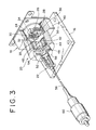
- the laser diode module is constructed by integrating a laser diode assembly (which will be hereinafter referred to as LD assembly) 18 fixed on a base 16, an optical isolator 20, and a fiber assembly 22.
- the LD assembly 18 includes a Peltier device 26 mounted on a metal stem 24.
- a metal carrier 28 having a good heat conductivity is mounted on the Peltier device 26.
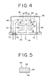
- On the carrier 28 are fixedly mounted a laser diode chip (which will be hereinafter referred to as LD chip) 30, a thermistor, and a relay block both not shown in Fig. 3 but will be described with reference to Fig. 4.
- LD chip laser diode chip
- a lens 32 for generally collimating light forwardly emitted from the LD chip 30 is fixed to the carrier 28.
- a photodiode 34 for detecting light backwardly emitted from the LD chip 30 is mounted on the stem 24.
- a cap 36 having a window 38 for transmitting the light forwardly emitted from the LD chip 30 is fixed to the stem 24 so as to sealingly enclose the inside of the LD assembly 18.
- the LD assembly 18 sealingly enclosed by the cap 36 and the stem 24 is accommodated in a frame 40.
- the optical isolator 20 includes a prism 42 formed of a birefringent crystal such as rutile, a Faraday rotator 44 formed of a magneto-optical crystal such as YIG (yttrium-iron-garnet), a prism 46 similar to the prism 42, and an annular permanent magnet 48 provided around the prisms 42 and 46 and the Faraday rotator 44 for applying a predetermined magnetic field to the Faraday rotator 44 in an advancing direction of the light.
- the prisms 42 and 46, the Faraday rotator 44, and the permanent magnet 48 are fixed in a frame 50 by a suitable means.
- the fiber assembly 22 is constructed by integrating a lens holder 54 for holding a lens 52 and a fiber holder 58 for holding an optical fiber 56.
- An optical connector 60 is fixed to one end of the optical fiber 56.
- the light emitted through the window 38 of the LD assembly 18 is transmitted through the optical isolator 20 with a high transmittance in a forward direction, and is introduced into the optical fiber 56. Then, the light is transmitted through the optical fiber 56 to a receiving section.
- a reflected return light undesirably generated on one end surface or the like of the optical fiber in the optical connector 60 is eliminated by the optical isolator 20 with a high attenuation factor, and it is hardly returned to the LD assembly 18. Accordingly, it is possible to maintain a stable operation of the LD chip 30 and directly drive the LD chip 30 for modulation.
- the relay block 64 is constructed of a block body 82 formed of an electrical insulator having a good heat conductivity and a metal film 84 formed on upper and lower surfaces of the block body 82.
- the block body 82 is preferably formed of beryllia. Beryllia has a good workability, and it makes easy the formation of the metal film 84 on the block body 82.
- An optimum material for the metal film 84 to be formed on the block body 82 is gold in consideration of easy fixation of the relay block 64 itself to the carrier 28 and easy wire bonding onto the relay block 64.
- the stem 24 is provided with a terminal 66 for connecting the thermistor 62 to an external circuit provided outside the LD assembly 18, a terminal 68 for connecting the Peltier device 26 to a driving circuit provided outside the LD assembly 18, and a terminal 70 for connecting the LD chip 30 to a driving circuit provided outside the LD assembly 18.
- These terminals 66, 68 and 70 extend through the stem 24, and they are electrically insulated from the metal stem 24 by glass hermetic seals 72.
- a common earth terminal 74 is connected to the stem 24.
- the thermistor 62 and the relay block 64 are connected together by a bonding wire 76, and the relay block 64 and the terminal 66 are connected together by a bonding wire 78.
- the Peltier device 26 and the terminal 68 are connected together by a bonding wire 79, and the LD chip 30 and the terminal 70 are connected together by a bonding wire 80.
- the relay block 64 directly fixed on the carrier 28 is formed of a material having a good heat conductivity is to let heat having flown through the terminal 66 and the bonding wire 78 into the relay block 64 be absorbed by the Peltier device 26 (provided that an external temperature is relatively high), thereby preventing the heat having flown into the relay block 64 from flowing through the bonding wire 76 into the thermistor 62.
- the first preferred embodiment is suitable in the case that a fixed position of the thermistor 62 on the carrier 28 is relatively spaced apart from a fixed position of the relay block 64 on the carrier 28, and that the Peltier device 26 has a relatively large capacity.
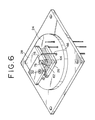
- the relay block 64 is constructed of a block body 82 formed of a heat insulating material and a metal film 84 formed on upper and lower surfaces of the block body 82.
- the relay block 64 is directly fixed to the stem 24 or the cap 36 so as not to contact the carrier 28.
- the block body 82 is preferably formed of alumina.
- the metal film 84 is optimally formed of gold similarly to the first preferred embodiment.
- the reason why the block body 82 of the relay block 64 is formed of a heat insulating material is as follows:
- the thermistor 62 and the relay block 64 are fixed to a side surface of the carrier 28.
- the LD chip 30 is also fixed to the side surface of the carrier 28 at a position below the lens 32.
- the relay block 64 is constructed of a block body 82 formed of a heat insulating material such as alumina, which is in the form of a rectangular parallelepiped, and a metal film 84 such as a gold film formed on the block body 82.
- the metal film 84 is formed on a surface of the block body 82 where the thermistor 62 and the terminal 66 are to be connected together by wire bonding, and the metal film 84 is also formed on another surface of the block body 82 where the relay block 64 is to be fixed to the carrier 28.
- connection points of the bonding wires 76 and 78 to the relay block 64 are located on different surfaces of the relay block 64, so as to make a wire bonding work easy.
- the reason why the relay block 64 is in contact with the carrier 28 in this preferred embodiment is to maintain the relay block 64 and the bonding wire 76 at the same temperature as that of the carrier 28 and the thermistor 62, thereby greatly suppressing the flow of heat through the bonding wire 76 into the thermistor 62 or the flow of heat out of the thermistor 62 through the bonding wire 76.
- the reason why the block body 82 of the relay block 64 is formed of a heat insulating material is to prevent the flow of heat between the carrier 28 and the outside of the LD assembly 18 and between the Peltier device 26 and the outside of the LD assembly 18 through the terminal 66 and the bonding wire 78. Accordingly, this preferred embodiment is especially suitable in the case that the carrier 28 and/or the Peltier device 26 has a small heat capacity.
- a connection point of the bonding wire 76 on the metal film 84 is spaced apart from a connection point of the bonding wire 78 on the metal film 84 as far as possible.
- Fig. 7B shows a modification of the relay block 64 to be employed in the third preferred embodiment for the purpose of minimizing the flow of the heat through the metal film 84 into or out of the thermistor 62. That is, the metal film 84 of the relay block 64 shown in Fig. 7B is relatively narrowed at a portion between the connection point of the bonding wire 76 on the metal film 84 and the connection point of the bonding wire 78 on the metal film 84. By reducing a width of the metal film 84 in this manner, a sectional area of the metal film 84 contributing to the flow of the heat through the metal film 84 into or out of the thermistor 62 is reduced to thereby minimize the flow of the heat through the metal film 84.
- a construction of the LD assembly 18 according to a fourth preferred embodiment of the present invention with reference to Figs. 8, 9A and 9B.
- two relay blocks 64A and 64B are fixed to the side surface of the carrier 28, and they are connected together by a bonding wire 81.
- the other construction in this preferred embodiment is the same as that in the third preferred embodiment shown in Fig. 6.
- the relay block 64A to be connected through the bonding wire 76 to the thermistor 62 is constructed of a metal body 86 having a good heat conductivity and an electrical insulator body 88 having a good heat conductivity.
- the metal body 86 is preferably formed of copper with a deposited gold film.
- a surface of the electrical insulator body 88 on the opposite side of the metal body 86 is deposited with gold for the purpose of fixing the relay block 64A to the carrier 28.
- the electrical insulator body 88 having a good heat conductivity is preferably formed of beryllia.
- the relay block 64B to be connected through the bonding wire 78 to the terminal 66 is constructed of a block body 82 formed of a heat insulating material and a metal film 84 formed on the block body 82.
- the block body 82 is preferably formed of alumina.
- the relay blocks 64A and 64B are connected together by the bonding wire 81.
- the flow of heat into the thermistor 62 or the flow of heat out of the thermistor 62 can be prevented very satisfactorily.
- the relay block 64A located in the proximity of the thermistor 62 is formed of a material having a good heat conductivity, a temperature of the thermistor 62 can be made substantially completely accord with a temperature of the carrier 28, thereby improving an accuracy of temperature control.
- the relay block 64B located in the proximity of the terminal 66 is primarily formed of a heat insulating material, the flow of heat into or out of the thermistor 62 can be effectively suppressed even when a temperature of the inside of the LD assembly 18 is remarkably different from a temperature of the outside of the LD assembly 18.
- the relay block located nearest to the thermistor 62 is formed from a composite body composed of a metal body and an electrical insulator body both having a good heat conductivity
- the relay block located nearest to the terminal 66 is constructed of a block body formed of a heat insulating material and a metal film formed on the block body.
- the present invention as mentioned above, it is possible to greatly prevent the flow of heat out of the thermistor through the terminal and the bonding wire to the outside of the LD assembly or the flow of heat from the outside of the LD assembly through the terminal and the bonding wire into the thermistor. Accordingly, the temperature of the thermistor will vary with the temperature of the LD chip, with the result that high-precision temperature control of the LD chip can be realized.
Landscapes
- Physics & Mathematics (AREA)
- General Physics & Mathematics (AREA)
- Optics & Photonics (AREA)
- Condensed Matter Physics & Semiconductors (AREA)
- Electromagnetism (AREA)
- Semiconductor Lasers (AREA)
- Optical Couplings Of Light Guides (AREA)
Applications Claiming Priority (2)
| Application Number | Priority Date | Filing Date | Title |
|---|---|---|---|
| JP187999/90 | 1990-07-18 | ||
| JP2187999A JP3035852B2 (ja) | 1990-07-18 | 1990-07-18 | 半導体レーザモジュール |
Publications (3)
| Publication Number | Publication Date |
|---|---|
| EP0467359A2 true EP0467359A2 (de) | 1992-01-22 |
| EP0467359A3 EP0467359A3 (en) | 1992-03-25 |
| EP0467359B1 EP0467359B1 (de) | 1994-10-19 |
Family
ID=16215870
Family Applications (1)
| Application Number | Title | Priority Date | Filing Date |
|---|---|---|---|
| EP91112022A Expired - Lifetime EP0467359B1 (de) | 1990-07-18 | 1991-07-18 | Laserdioden-Anordnung |
Country Status (4)
| Country | Link |
|---|---|
| US (1) | US5212699A (de) |
| EP (1) | EP0467359B1 (de) |
| JP (1) | JP3035852B2 (de) |
| DE (1) | DE69104661D1 (de) |
Cited By (3)
| Publication number | Priority date | Publication date | Assignee | Title |
|---|---|---|---|---|
| EP0762567A1 (de) * | 1995-08-18 | 1997-03-12 | Nec Corporation | Temperaturgeregelter Halbleiterlasergerät und Temperaturregelungsverfahren |
| EP1229315A1 (de) * | 2001-02-05 | 2002-08-07 | Fujitsu Quantum Devices Limited | Halbleiteranordnungsträger |
| WO2015116274A3 (en) * | 2013-11-05 | 2015-09-24 | Cisco Technology, Inc. | Method and system for an optical communication device |
Families Citing this family (37)
| Publication number | Priority date | Publication date | Assignee | Title |
|---|---|---|---|---|
| JPH0286051A (ja) * | 1988-09-20 | 1990-03-27 | Japan Storage Battery Co Ltd | 密閉形鉛蓄電池 |
| JPH0555710A (ja) * | 1991-08-23 | 1993-03-05 | Nec Corp | 半導体レーザモジユール |
| JPH05127050A (ja) * | 1991-10-30 | 1993-05-25 | Hitachi Ltd | 半導体レーザモジユール |
| US5383142A (en) * | 1993-10-01 | 1995-01-17 | Hewlett-Packard Company | Fast circuit and method for detecting predetermined bit patterns |
| US5400351A (en) * | 1994-05-09 | 1995-03-21 | Lumonics Inc. | Control of a pumping diode laser |
| JP2937791B2 (ja) * | 1995-03-14 | 1999-08-23 | 日本電気株式会社 | ペルチエクラーク |
| JPH0983082A (ja) * | 1995-09-19 | 1997-03-28 | Hitachi Ltd | 半導体レーザ素子及び光ディスク装置、並びに光軸調整方法 |
| US5898211A (en) * | 1996-04-30 | 1999-04-27 | Cutting Edge Optronics, Inc. | Laser diode package with heat sink |
| US5734672A (en) * | 1996-08-06 | 1998-03-31 | Cutting Edge Optronics, Inc. | Smart laser diode array assembly and operating method using same |
| JP3076246B2 (ja) * | 1996-08-13 | 2000-08-14 | 日本電気株式会社 | ペルチェクーラ内蔵半導体レーザモジュール |
| JP3830583B2 (ja) * | 1996-08-15 | 2006-10-04 | 富士通株式会社 | 光半導体アセンブリ |
| US5913108A (en) * | 1998-04-30 | 1999-06-15 | Cutting Edge Optronics, Inc. | Laser diode packaging |
| US6636538B1 (en) * | 1999-03-29 | 2003-10-21 | Cutting Edge Optronics, Inc. | Laser diode packaging |
| TW449948B (en) * | 1999-06-29 | 2001-08-11 | Rohm Co Ltd | Semiconductor device |
| JP4074419B2 (ja) * | 2000-03-14 | 2008-04-09 | シャープ株式会社 | 半導体レーザ装置のワイヤボンディング方法 |
| US6700913B2 (en) | 2001-05-29 | 2004-03-02 | Northrop Grumman Corporation | Low cost high integrity diode laser array |
| JP2004079989A (ja) * | 2002-04-04 | 2004-03-11 | Furukawa Electric Co Ltd:The | 光モジュール |
| US7403347B2 (en) | 2002-04-04 | 2008-07-22 | The Furukawa Electric Co., Ltd. | Optical transmission module with temperature control |
| US7170919B2 (en) * | 2003-06-23 | 2007-01-30 | Northrop Grumman Corporation | Diode-pumped solid-state laser gain module |
| US7192201B2 (en) * | 2003-07-09 | 2007-03-20 | Sumitomo Electric Industries, Ltd. | Optical transmitting module having a de-coupling inductor therein |
| US7218657B2 (en) * | 2003-07-09 | 2007-05-15 | Sumitomo Electric Industries, Ltd. | Optical transmitting module having a can type package and providing a temperature sensor therein |
| US7495848B2 (en) * | 2003-07-24 | 2009-02-24 | Northrop Grumman Corporation | Cast laser optical bench |
| US7305016B2 (en) | 2005-03-10 | 2007-12-04 | Northrop Grumman Corporation | Laser diode package with an internal fluid cooling channel |
| US7856038B2 (en) | 2006-03-27 | 2010-12-21 | Sumitomo Electric Industries, Ltd. | Light-emitting module installing thermo-electric controller |
| JP4772560B2 (ja) * | 2006-03-31 | 2011-09-14 | 住友電工デバイス・イノベーション株式会社 | 光半導体装置、およびその制御方法 |
| US7656915B2 (en) * | 2006-07-26 | 2010-02-02 | Northrop Grumman Space & Missions Systems Corp. | Microchannel cooler for high efficiency laser diode heat extraction |
| US20080056314A1 (en) * | 2006-08-31 | 2008-03-06 | Northrop Grumman Corporation | High-power laser-diode package system |
| US7724791B2 (en) * | 2008-01-18 | 2010-05-25 | Northrop Grumman Systems Corporation | Method of manufacturing laser diode packages and arrays |
| US8345720B2 (en) * | 2009-07-28 | 2013-01-01 | Northrop Grumman Systems Corp. | Laser diode ceramic cooler having circuitry for control and feedback of laser diode performance |
| US8811439B2 (en) * | 2009-11-23 | 2014-08-19 | Seminex Corporation | Semiconductor laser assembly and packaging system |
| US9590388B2 (en) | 2011-01-11 | 2017-03-07 | Northrop Grumman Systems Corp. | Microchannel cooler for a single laser diode emitter based system |
| KR101291715B1 (ko) * | 2011-05-19 | 2013-07-31 | 주식회사 포벨 | 써미스터를 이용한 온도 측정 방법 |
| US8937976B2 (en) | 2012-08-15 | 2015-01-20 | Northrop Grumman Systems Corp. | Tunable system for generating an optical pulse based on a double-pass semiconductor optical amplifier |
| JPWO2017221441A1 (ja) * | 2016-06-20 | 2018-06-21 | 三菱電機株式会社 | 光通信デバイス |
| CN109041552A (zh) * | 2018-10-12 | 2018-12-18 | 成都优博创通信技术股份有限公司 | 一种散热组件及通信模块 |
| CN109407226B (zh) * | 2018-11-23 | 2020-11-10 | 武汉电信器件有限公司 | 一种高速eml同轴发射组件及其制作方法 |
| WO2022230053A1 (ja) * | 2021-04-27 | 2022-11-03 | 三菱電機株式会社 | 半導体レーザ光源装置 |
Citations (5)
| Publication number | Priority date | Publication date | Assignee | Title |
|---|---|---|---|---|
| JPS5923583A (ja) * | 1982-07-30 | 1984-02-07 | Canon Inc | レ−ザユニツト |
| EP0100086A2 (de) * | 1982-07-27 | 1984-02-08 | Stc Plc | Verfahren zur Herstellung von Einkapselungen von Laserdioden und Einkapselungen, die nach einem solchen Verfahren hergestellt sind |
| US4571728A (en) * | 1982-04-09 | 1986-02-18 | Olympus Optical Co., Ltd. | Temperature control device for a semiconductor laser |
| US4792957A (en) * | 1986-12-22 | 1988-12-20 | Gte Communication Systems Corporation | Laser temperature controller |
| EP0326207A1 (de) * | 1988-01-22 | 1989-08-02 | Koninklijke Philips Electronics N.V. | Laserdiodenmodul |
Family Cites Families (8)
| Publication number | Priority date | Publication date | Assignee | Title |
|---|---|---|---|---|
| JPS5946434B2 (ja) * | 1978-01-10 | 1984-11-12 | キヤノン株式会社 | 半導体レ−ザ装置 |
| US4399541A (en) * | 1981-02-17 | 1983-08-16 | Northern Telecom Limited | Light emitting device package having combined heater/cooler |
| JPS6171689A (ja) * | 1984-09-17 | 1986-04-12 | Hitachi Ltd | 半導体レ−ザ装置 |
| JPH0634424B2 (ja) * | 1986-07-18 | 1994-05-02 | 三菱電機株式会社 | 光結合装置 |
| JPS6370589A (ja) * | 1986-09-12 | 1988-03-30 | Nec Corp | 半導体レ−ザモジユ−ル |
| JPH01245585A (ja) * | 1988-03-26 | 1989-09-29 | Nec Corp | 半導体レーザ装置 |
| JPH01318275A (ja) * | 1988-06-20 | 1989-12-22 | Nec Corp | 半導体レーザ装置 |
| US5068865A (en) * | 1988-06-09 | 1991-11-26 | Nec Corporation | Semiconductor laser module |
-
1990
- 1990-07-18 JP JP2187999A patent/JP3035852B2/ja not_active Expired - Lifetime
-
1991
- 1991-07-15 US US07/729,997 patent/US5212699A/en not_active Expired - Lifetime
- 1991-07-18 DE DE69104661T patent/DE69104661D1/de not_active Expired - Lifetime
- 1991-07-18 EP EP91112022A patent/EP0467359B1/de not_active Expired - Lifetime
Patent Citations (5)
| Publication number | Priority date | Publication date | Assignee | Title |
|---|---|---|---|---|
| US4571728A (en) * | 1982-04-09 | 1986-02-18 | Olympus Optical Co., Ltd. | Temperature control device for a semiconductor laser |
| EP0100086A2 (de) * | 1982-07-27 | 1984-02-08 | Stc Plc | Verfahren zur Herstellung von Einkapselungen von Laserdioden und Einkapselungen, die nach einem solchen Verfahren hergestellt sind |
| JPS5923583A (ja) * | 1982-07-30 | 1984-02-07 | Canon Inc | レ−ザユニツト |
| US4792957A (en) * | 1986-12-22 | 1988-12-20 | Gte Communication Systems Corporation | Laser temperature controller |
| EP0326207A1 (de) * | 1988-01-22 | 1989-08-02 | Koninklijke Philips Electronics N.V. | Laserdiodenmodul |
Non-Patent Citations (1)
| Title |
|---|
| PATENT ABSTRACTS OF JAPAN vol. 8, no. 107 (E-245)(1544) 19 May 1984 & JP-A-59 023 583 ( CANON K.K. ) 7 February 1984 * |
Cited By (8)
| Publication number | Priority date | Publication date | Assignee | Title |
|---|---|---|---|---|
| EP0762567A1 (de) * | 1995-08-18 | 1997-03-12 | Nec Corporation | Temperaturgeregelter Halbleiterlasergerät und Temperaturregelungsverfahren |
| EP1229315A1 (de) * | 2001-02-05 | 2002-08-07 | Fujitsu Quantum Devices Limited | Halbleiteranordnungsträger |
| US6975031B2 (en) | 2001-02-05 | 2005-12-13 | Fujitsu Quantum Devices Limited | Semiconductor device and chip carrier |
| WO2015116274A3 (en) * | 2013-11-05 | 2015-09-24 | Cisco Technology, Inc. | Method and system for an optical communication device |
| CN105705975A (zh) * | 2013-11-05 | 2016-06-22 | 思科技术公司 | 用于光学通信设备的方法和系统 |
| US9628184B2 (en) | 2013-11-05 | 2017-04-18 | Cisco Technology, Inc. | Efficient optical communication device |
| US9755752B2 (en) | 2013-11-05 | 2017-09-05 | Cisco Technology, Inc. | Method for manufacturing an optical communication device |
| US10735101B2 (en) | 2013-11-05 | 2020-08-04 | Cisco Technology, Inc. | Method for manufacturing an optical communication device |
Also Published As
| Publication number | Publication date |
|---|---|
| EP0467359B1 (de) | 1994-10-19 |
| JPH0475394A (ja) | 1992-03-10 |
| EP0467359A3 (en) | 1992-03-25 |
| US5212699A (en) | 1993-05-18 |
| JP3035852B2 (ja) | 2000-04-24 |
| DE69104661D1 (de) | 1994-11-24 |
Similar Documents
| Publication | Publication Date | Title |
|---|---|---|
| EP0467359B1 (de) | Laserdioden-Anordnung | |
| US6490303B1 (en) | Laser diode module | |
| US7210859B2 (en) | Optoelectronic components with multi-layer feedthrough structure | |
| US4722586A (en) | Electro-optical transducer module | |
| US5706302A (en) | Temperature control type semiconductor laser device | |
| EP0477841B1 (de) | Laserdiodenmodul und Verfahren zu seiner Herstellung | |
| US6404042B1 (en) | Subcarrier and semiconductor device | |
| GB2131607A (en) | Semiconductor laser device | |
| EP0824281B1 (de) | Peltierkühler und Verwendung in einem Halbleiterlasermodul | |
| EP0619507B1 (de) | Optoelektronisches Modul mit Kopplung zwischen einer optoelektronischen Komponente, insbesondere einem Halbleiterlaser, und einer optischen Glasfaser, und Methode seiner Herstellung | |
| JPWO2021014568A1 (ja) | To−can型光送信モジュール | |
| US7403347B2 (en) | Optical transmission module with temperature control | |
| JPH11186668A (ja) | 光半導体モジュール | |
| EP0556639B1 (de) | Halbleiterlaservorrichtung | |
| JPH04112591A (ja) | 半導体レーザモジュール | |
| US20030012525A1 (en) | Light-emitting module | |
| JPH0569406B2 (de) | ||
| JP2001284700A (ja) | 半導体レーザモジュール | |
| JPH02197185A (ja) | 電子式冷却素子内蔵半導体レーザアセンブリ | |
| JP2783036B2 (ja) | 半導体レーザモジュール | |
| JP2005064483A (ja) | 発光モジュール | |
| JPS61234588A (ja) | 光半導体素子用サブマウント | |
| JPH04243181A (ja) | 半導体レーザモジュール | |
| JPH0497581A (ja) | 半導体レーザのヒートシンク | |
| JP2599226Y2 (ja) | 光送信モジュール |
Legal Events
| Date | Code | Title | Description |
|---|---|---|---|
| PUAI | Public reference made under article 153(3) epc to a published international application that has entered the european phase |
Free format text: ORIGINAL CODE: 0009012 |
|
| AK | Designated contracting states |
Kind code of ref document: A2 Designated state(s): DE FR GB IT NL |
|
| PUAL | Search report despatched |
Free format text: ORIGINAL CODE: 0009013 |
|
| AK | Designated contracting states |
Kind code of ref document: A3 Designated state(s): DE FR GB IT NL |
|
| 17P | Request for examination filed |
Effective date: 19920512 |
|
| 17Q | First examination report despatched |
Effective date: 19931124 |
|
| GRAA | (expected) grant |
Free format text: ORIGINAL CODE: 0009210 |
|
| AK | Designated contracting states |
Kind code of ref document: B1 Designated state(s): DE FR GB IT NL |
|
| PG25 | Lapsed in a contracting state [announced via postgrant information from national office to epo] |
Ref country code: IT Free format text: LAPSE BECAUSE OF FAILURE TO SUBMIT A TRANSLATION OF THE DESCRIPTION OR TO PAY THE FEE WITHIN THE PRE;WARNING: LAPSES OF ITALIAN PATENTS WITH EFFECTIVE DATE BEFORE 2007 MAY HAVE OCCURRED AT ANY TIME BEFORE 2007. THE CORRECT EFFECTIVE DATE MAY BE DIFFERENT FROM THE ONE RECORDED.SCRIBED TIME-LIMIT Effective date: 19941019 Ref country code: FR Effective date: 19941019 Ref country code: NL Effective date: 19941019 |
|
| REF | Corresponds to: |
Ref document number: 69104661 Country of ref document: DE Date of ref document: 19941124 |
|
| PG25 | Lapsed in a contracting state [announced via postgrant information from national office to epo] |
Ref country code: DE Effective date: 19950120 |
|
| NLV1 | Nl: lapsed or annulled due to failure to fulfill the requirements of art. 29p and 29m of the patents act | ||
| EN | Fr: translation not filed | ||
| PLBE | No opposition filed within time limit |
Free format text: ORIGINAL CODE: 0009261 |
|
| STAA | Information on the status of an ep patent application or granted ep patent |
Free format text: STATUS: NO OPPOSITION FILED WITHIN TIME LIMIT |
|
| 26N | No opposition filed | ||
| REG | Reference to a national code |
Ref country code: GB Ref legal event code: IF02 |
|
| PGFP | Annual fee paid to national office [announced via postgrant information from national office to epo] |
Ref country code: GB Payment date: 20070718 Year of fee payment: 17 |
|
| GBPC | Gb: european patent ceased through non-payment of renewal fee |
Effective date: 20080718 |
|
| PG25 | Lapsed in a contracting state [announced via postgrant information from national office to epo] |
Ref country code: GB Free format text: LAPSE BECAUSE OF NON-PAYMENT OF DUE FEES Effective date: 20080718 |