EP0430593B1 - Procédé pour couper un substrat en silicium utilisant une attaque préférentielle - Google Patents
Procédé pour couper un substrat en silicium utilisant une attaque préférentielle Download PDFInfo
- Publication number
- EP0430593B1 EP0430593B1 EP90312750A EP90312750A EP0430593B1 EP 0430593 B1 EP0430593 B1 EP 0430593B1 EP 90312750 A EP90312750 A EP 90312750A EP 90312750 A EP90312750 A EP 90312750A EP 0430593 B1 EP0430593 B1 EP 0430593B1
- Authority
- EP
- European Patent Office
- Prior art keywords
- wafer
- etch
- recess
- etching
- opening
- Prior art date
- Legal status (The legal status is an assumption and is not a legal conclusion. Google has not performed a legal analysis and makes no representation as to the accuracy of the status listed.)
- Expired - Lifetime
Links
- 238000000034 method Methods 0.000 title claims description 54
- 238000005530 etching Methods 0.000 title claims description 47
- XUIMIQQOPSSXEZ-UHFFFAOYSA-N Silicon Chemical compound [Si] XUIMIQQOPSSXEZ-UHFFFAOYSA-N 0.000 title claims description 33
- 229910052710 silicon Inorganic materials 0.000 title claims description 30
- 239000010703 silicon Substances 0.000 title claims description 30
- 230000001419 dependent effect Effects 0.000 title claims description 11
- 238000005520 cutting process Methods 0.000 title description 2
- 238000004519 manufacturing process Methods 0.000 claims description 18
- 238000007641 inkjet printing Methods 0.000 claims description 3
- 230000001154 acute effect Effects 0.000 claims 1
- 235000012431 wafers Nutrition 0.000 description 129
- 229910052581 Si3N4 Inorganic materials 0.000 description 11
- HQVNEWCFYHHQES-UHFFFAOYSA-N silicon nitride Chemical compound N12[Si]34N5[Si]62N3[Si]51N64 HQVNEWCFYHHQES-UHFFFAOYSA-N 0.000 description 11
- 239000000463 material Substances 0.000 description 6
- 238000003491 array Methods 0.000 description 4
- 238000002161 passivation Methods 0.000 description 4
- 238000001020 plasma etching Methods 0.000 description 4
- 239000000758 substrate Substances 0.000 description 4
- CSDREXVUYHZDNP-UHFFFAOYSA-N alumanylidynesilicon Chemical compound [Al].[Si] CSDREXVUYHZDNP-UHFFFAOYSA-N 0.000 description 3
- 239000013078 crystal Substances 0.000 description 3
- 238000000059 patterning Methods 0.000 description 3
- OKTJSMMVPCPJKN-UHFFFAOYSA-N Carbon Chemical compound [C] OKTJSMMVPCPJKN-UHFFFAOYSA-N 0.000 description 2
- NBIIXXVUZAFLBC-UHFFFAOYSA-N Phosphoric acid Chemical compound OP(O)(O)=O NBIIXXVUZAFLBC-UHFFFAOYSA-N 0.000 description 2
- 230000015572 biosynthetic process Effects 0.000 description 2
- YCIMNLLNPGFGHC-UHFFFAOYSA-N catechol Chemical compound OC1=CC=CC=C1O YCIMNLLNPGFGHC-UHFFFAOYSA-N 0.000 description 2
- 238000005229 chemical vapour deposition Methods 0.000 description 2
- 238000006073 displacement reaction Methods 0.000 description 2
- 229910002804 graphite Inorganic materials 0.000 description 2
- 239000010439 graphite Substances 0.000 description 2
- 230000000873 masking effect Effects 0.000 description 2
- 238000000926 separation method Methods 0.000 description 2
- 229910000147 aluminium phosphate Inorganic materials 0.000 description 1
- 230000009286 beneficial effect Effects 0.000 description 1
- 239000011248 coating agent Substances 0.000 description 1
- 238000000576 coating method Methods 0.000 description 1
- 238000004891 communication Methods 0.000 description 1
- 229910021419 crystalline silicon Inorganic materials 0.000 description 1
- 239000002019 doping agent Substances 0.000 description 1
- 230000000694 effects Effects 0.000 description 1
- 239000010408 film Substances 0.000 description 1
- 239000007943 implant Substances 0.000 description 1
- 230000010354 integration Effects 0.000 description 1
- 238000010884 ion-beam technique Methods 0.000 description 1
- 150000002500 ions Chemical class 0.000 description 1
- 229910044991 metal oxide Inorganic materials 0.000 description 1
- 150000004706 metal oxides Chemical class 0.000 description 1
- 229910021421 monocrystalline silicon Inorganic materials 0.000 description 1
- 239000002245 particle Substances 0.000 description 1
- 239000010409 thin film Substances 0.000 description 1
- 238000001039 wet etching Methods 0.000 description 1
Images


Classifications
-
- B—PERFORMING OPERATIONS; TRANSPORTING
- B41—PRINTING; LINING MACHINES; TYPEWRITERS; STAMPS
- B41J—TYPEWRITERS; SELECTIVE PRINTING MECHANISMS, i.e. MECHANISMS PRINTING OTHERWISE THAN FROM A FORME; CORRECTION OF TYPOGRAPHICAL ERRORS
- B41J2/00—Typewriters or selective printing mechanisms characterised by the printing or marking process for which they are designed
- B41J2/005—Typewriters or selective printing mechanisms characterised by the printing or marking process for which they are designed characterised by bringing liquid or particles selectively into contact with a printing material
- B41J2/01—Ink jet
- B41J2/135—Nozzles
- B41J2/16—Production of nozzles
- B41J2/1601—Production of bubble jet print heads
- B41J2/1603—Production of bubble jet print heads of the front shooter type
-
- B—PERFORMING OPERATIONS; TRANSPORTING
- B41—PRINTING; LINING MACHINES; TYPEWRITERS; STAMPS
- B41J—TYPEWRITERS; SELECTIVE PRINTING MECHANISMS, i.e. MECHANISMS PRINTING OTHERWISE THAN FROM A FORME; CORRECTION OF TYPOGRAPHICAL ERRORS
- B41J2/00—Typewriters or selective printing mechanisms characterised by the printing or marking process for which they are designed
- B41J2/005—Typewriters or selective printing mechanisms characterised by the printing or marking process for which they are designed characterised by bringing liquid or particles selectively into contact with a printing material
- B41J2/01—Ink jet
- B41J2/135—Nozzles
- B41J2/16—Production of nozzles
- B41J2/1621—Manufacturing processes
- B41J2/1626—Manufacturing processes etching
- B41J2/1628—Manufacturing processes etching dry etching
-
- B—PERFORMING OPERATIONS; TRANSPORTING
- B41—PRINTING; LINING MACHINES; TYPEWRITERS; STAMPS
- B41J—TYPEWRITERS; SELECTIVE PRINTING MECHANISMS, i.e. MECHANISMS PRINTING OTHERWISE THAN FROM A FORME; CORRECTION OF TYPOGRAPHICAL ERRORS
- B41J2/00—Typewriters or selective printing mechanisms characterised by the printing or marking process for which they are designed
- B41J2/005—Typewriters or selective printing mechanisms characterised by the printing or marking process for which they are designed characterised by bringing liquid or particles selectively into contact with a printing material
- B41J2/01—Ink jet
- B41J2/135—Nozzles
- B41J2/16—Production of nozzles
- B41J2/1621—Manufacturing processes
- B41J2/1626—Manufacturing processes etching
- B41J2/1629—Manufacturing processes etching wet etching
-
- H—ELECTRICITY
- H01—ELECTRIC ELEMENTS
- H01L—SEMICONDUCTOR DEVICES NOT COVERED BY CLASS H10
- H01L21/00—Processes or apparatus adapted for the manufacture or treatment of semiconductor or solid state devices or of parts thereof
- H01L21/02—Manufacture or treatment of semiconductor devices or of parts thereof
- H01L21/04—Manufacture or treatment of semiconductor devices or of parts thereof the devices having at least one potential-jump barrier or surface barrier, e.g. PN junction, depletion layer or carrier concentration layer
- H01L21/18—Manufacture or treatment of semiconductor devices or of parts thereof the devices having at least one potential-jump barrier or surface barrier, e.g. PN junction, depletion layer or carrier concentration layer the devices having semiconductor bodies comprising elements of Group IV of the Periodic System or AIIIBV compounds with or without impurities, e.g. doping materials
- H01L21/30—Treatment of semiconductor bodies using processes or apparatus not provided for in groups H01L21/20 - H01L21/26
- H01L21/302—Treatment of semiconductor bodies using processes or apparatus not provided for in groups H01L21/20 - H01L21/26 to change their surface-physical characteristics or shape, e.g. etching, polishing, cutting
- H01L21/306—Chemical or electrical treatment, e.g. electrolytic etching
- H01L21/30604—Chemical etching
- H01L21/30608—Anisotropic liquid etching
-
- H—ELECTRICITY
- H01—ELECTRIC ELEMENTS
- H01L—SEMICONDUCTOR DEVICES NOT COVERED BY CLASS H10
- H01L21/00—Processes or apparatus adapted for the manufacture or treatment of semiconductor or solid state devices or of parts thereof
- H01L21/02—Manufacture or treatment of semiconductor devices or of parts thereof
- H01L21/04—Manufacture or treatment of semiconductor devices or of parts thereof the devices having at least one potential-jump barrier or surface barrier, e.g. PN junction, depletion layer or carrier concentration layer
- H01L21/18—Manufacture or treatment of semiconductor devices or of parts thereof the devices having at least one potential-jump barrier or surface barrier, e.g. PN junction, depletion layer or carrier concentration layer the devices having semiconductor bodies comprising elements of Group IV of the Periodic System or AIIIBV compounds with or without impurities, e.g. doping materials
- H01L21/30—Treatment of semiconductor bodies using processes or apparatus not provided for in groups H01L21/20 - H01L21/26
- H01L21/302—Treatment of semiconductor bodies using processes or apparatus not provided for in groups H01L21/20 - H01L21/26 to change their surface-physical characteristics or shape, e.g. etching, polishing, cutting
- H01L21/306—Chemical or electrical treatment, e.g. electrolytic etching
- H01L21/308—Chemical or electrical treatment, e.g. electrolytic etching using masks
- H01L21/3081—Chemical or electrical treatment, e.g. electrolytic etching using masks characterised by their composition, e.g. multilayer masks, materials
-
- H—ELECTRICITY
- H01—ELECTRIC ELEMENTS
- H01L—SEMICONDUCTOR DEVICES NOT COVERED BY CLASS H10
- H01L21/00—Processes or apparatus adapted for the manufacture or treatment of semiconductor or solid state devices or of parts thereof
- H01L21/70—Manufacture or treatment of devices consisting of a plurality of solid state components formed in or on a common substrate or of parts thereof; Manufacture of integrated circuit devices or of parts thereof
- H01L21/71—Manufacture of specific parts of devices defined in group H01L21/70
- H01L21/768—Applying interconnections to be used for carrying current between separate components within a device comprising conductors and dielectrics
- H01L21/76898—Applying interconnections to be used for carrying current between separate components within a device comprising conductors and dielectrics formed through a semiconductor substrate
Definitions
- This invention relates to methods of precisely forming through holes in (100) silicon wafers by orientation dependent etching (ODE) either before or after fabrication of the integrated circuit on the wafer. More specifically, the invention involves ODE to fabricate integrated circuit (IC) wafer subunits having precision through holes which define butt edges or surfaces for forming a butted array of subunits.
- ODE orientation dependent etching
- the ability to precisely locate and dimension butt edges or surfaces of IC wafer subunits (or chips) finds use in the precision delineation of these wafer subunits for any extended array using subunit modules.
- Wafer subunits are aligned in extended arrays to form, e.g., pagewidth printheads for inkjet type printers, or RIS and ROS arrays.
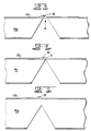
- a fundamental problem with etching only through the back surface of the wafer is that the width of the opening on the unetched upper surface is a function of the wafer thickness. Since it is not uncommon for wafers to have variations in thickness, it has not been possible to precisely locate openings on the circuit side of the wafer. For example, if the etch mask is designed to produce a through hole H adjacent the integrated circuit IC and just reaching the upper integrated circuit surface CS of a 508 ⁇ m thick wafer W 1 (see Fig. 1B), it will actually produce a 35.6 ⁇ m wide opening on a 483 ⁇ m thick wafer W 2 (Fig. 1A) and will not produce any opening at all on a 533 ⁇ m thick wafer W 3 (Fig. 1C).
- Kurth discloses a method of forming an ink jet nozzle in a (100) silicon wafer by etching through obverse and reverse surfaces of the wafer. The method does not produce butt edges and is not performed after integration circuit fabrication on the wafer.
- the etch resistant layer used by Kurth'008 is not plasma silicon nitride.
- Thermal ink jet printers contain printheads, such as roofshooter printheads shown in Figure 2 and described in US-A-4,789,425 to Drake et al.
- the printheads are constructed from silicon wafer subunits (or chips) 1 which include nozzles 2, reservoirs 3 for conducting ink to the nozzle outlets and integrated circuitry 4.
- the integrated circuitry includes a resistive heater element which responds to an electrical impulse to vaporize a portion of the ink in a passageway 6 which provides the motive force to form an ink drop which is expelled onto a recording medium.
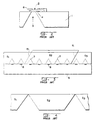
- Some printheads such as sideshooter printheads shown in Figure 3 and described in US-A-4,601,777 to Hawkins et al, are formed from a number of wafer subunits S 1 , S 2 , S 3 butted together and layered upon a support substrate.
- the sideshooter printhead includes nozzles 7 and resistive heater element circuit 8 located on a heater substrate 9 for controlling ink output from each nozzle 7.
- the printhead is wired to a daughter board, placed in communication with a source of ink and mounted on a carriage of an ink jet printer for reciprocation across the surface of a recording medium, such as paper.
- a pagewidth array of wafer subunits can be formed by butting together a plurality of subunits S 1 , S 2 , S 3 into the length of a pagewidth.
- the array is fixed and the recording medium moves at a constant velocity in a direction perpendicular to the array.
- the current practice is to form the nozzles, passageways and integrated circuitry on silicon wafers, separate these wafers into wafer subunits (or chips) which contain butt surfaces or edges, align these subunits along their butt surfaces or edges into an array having a length of a pagewidth, and attach the array to a substrate to form a pagewidth printhead.
- the layering of the wafers, if necessary, to form the complete printhead can be performed before or after separation into subunits. Since many wafer subunits are aligned to form an array, each subunit must be uniform.
- the location of the butt edges or surfaces relative to the circuitry must be precise. Additionally, since the step of separating a wafer into subunits is performed as a batch, well prior to the step of aligning the subunits into arrays, the later step usually involves selecting subunits from a bin which contains subunits having a variety of thicknesses. When the subunits S 1 , S 2 are formed with diagonal butt surfaces, a difference in height ⁇ h between adjacent subunits results in a lateral shift 0.7 ⁇ h of the circuit surfaces CS of these subunits (see Figure 5).
- FIG. 6A-6B One previous technique for forming butt edges, shown in Figures 6A-6B, involves orientation dependent etching a groove 10 on one surface of the wafer, placing a dice cut 11 in the opposite surface of the wafer and applying a force F to fracture break the wafer along line 12 into subunits to produce butt edges 13. Adjacent subunits are then butted together at the butt edges 13 (Fig. 6B). Disadvantages of this technique are: the fracture edges can produce cracked passivation up to 50 micrometers away, the butt edges 13 are razor edges which are easily damaged, and any difference in chip thickness ⁇ h between two subunits results in a lateral shift of 0.7 ⁇ h of one chip surface relative to the other. The lateral shift is due to the angle of the (111) etched surfaces.
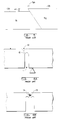
- FIG. 3 Another previous method for forming butt surfaces, illustrated in Figure 3, involves orientation dependent etching troughs entirely through the wafer, giving a parallelogram cross section to the wafer.
- the butt surfaces 15, 16 are crystal (111) planes.
- Advantages of this method are (1) the butt surfaces are formed gently by wet etching, and (2) the butt surface is a robust crystal plane.
- a disadvantage is that two separate through etches are required and the area between the butted surfaces is so large that dirt particles can prevent intimate butting.
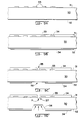
- FIGs 7A and 7B Another previous method, illustrated in Figures 7A and 7B, which requires only one through etch, involves making at least one through etch 20 on one surface of the wafer to define a first butt edge 21 and dividing the wafer into DIE 1 and DIE 2, forming a trough 22 on the other surface of the wafer, and then making a dice cut 23 through the trough 22 to form a second butt edge 24.
- the first butt edge 21 of each subunit is butted against the second butt edge 24 of an adjacent subunit (Fig. 7B) to form the array.
- This method reduces the amount of etch time required and also reduces the butt edge area.
- a dice cut is required, it is possible to produce cracked passivation.
- This method also is susceptible to a lateral displacement of 0.7 ⁇ h due to differences in adjacent chip height ⁇ h.
- a further previous method involves producing butt edges by reactive ion etching (RIE) from the circuit surface to a groove G cut into the base surface.
- RIE reactive ion etching
- This method is advantageous in that it produces vertical butt surfaces 25, 26 and thus differences in the height of adjacent butting chips do not result in lateral displacements.
- a disadvantage is that the RIE trenches must be etched prior to metal oxide silicon (MOS) fabrication due to potential oxide damage from the high energy ions.
- MOS metal oxide silicon
- US-A-4,601,777 to Hawkins et al discloses thermal ink jet printheads which are formed in (100) silicon wafers.
- the wafers can be separated into subunits to form printheads and the printheads can be aligned into pagewidth arrays.
- the wafers are separated into printheads by dicing.
- US-A-4,612,554 to Poleshuk discloses a thermal ink jet printhead and method of making same.
- the printheads are formed from (100) silicon wafers on which the integrated circuits are fabricated after application of an etch resistant pyrolytic silicon nitride layer.
- Poleshuk discloses dicing to form butt edges.
- US-A-4,784,721 to Holmen et al discloses a process for fabricating a thin film microsensor for airflow. The process only etches through a back surface of a (100) silicon wafer, does not provide a through hole in the wafer and does not discuss the fabrication of butt edges.
- T.S. Kuan et al. in IBM Technical Disclosure Bulletin Vol. 21, No. 6, November 1978, pp.2585-2586 discloses a two sided groove etching method to produce silicon ink jet nozzles.
- the method involves (pyrocatechol) etching a groove defined by (111) surfaces in opposing surfaces of a (100) Si wafer, the etching commencing at points directly opposite each other so that the grooves eventually join up in the middle of the wafer.
- Another object of the present invention is to fabricate pagewidth printheads by precisely aligning adjacent (100) silicon wafer subunits.
- a method of separating one or more subunits from a silicon wafer having a (100) crystallographic orientation comprising: anisotropically etching the wafer by orientation dependent etching through at least one pair of etch openings corresponding to the boundaries of the subunits and being formed in etch resistant layers on the upper and lower face of the wafer, respectively, wherein the or each etch opening in the etch resistant layer on lower face is substantially vertically aligned within a predetermined tolerance with a respective space etch opening in the etch resistant layer on the upper face, thereby forming at least one pair of parallel, aligned recesses at the etch openings, the recesses being bounded by surfaces lying in planes having a (111) crystallographic orientation, the width of the etch openings of each pair being such that the etched recesses each have a depth less than the thickness of the wafer but each pair of parallel, aligned recesses intersects within the thickness of the wafer
- the invention further provides a method of mounting subunits in a linear array, according to claims 7, 8 and 9 of the appended claims.
- the invention further comprises a method of fabricating a printhead for an ink jet printing apparatus, according to claim 10 of the appended claims.
- the present invention preferably makes use of an etchant material, e.g., plasma silicon nitride, which can be applied at a relatively low temperature between 250°C and 450°C, which enables masking of the IC side of the wafer without silicon-aluminum interdiffusion.
- an etchant material e.g., plasma silicon nitride
- an integrated circuit is fabricated on a (100) silicon wafer.
- an etch resistant layer is applied on circuit and base surfaces of the wafer. These etch resistant layers are patterned to form upper and lower etch openings and the wafer is anisotropically etched to form upper and lower recesses which correspond to the upper and lower etch openings. These upper and lower recesses intersect one another to form a through opening which is precisely aligned with the integrated circuitry on the wafer.
- the wafer can then be separated along the through holes to form wafersubunits (or chips) which have precisely defined butt edges. These butt edges are formed without dicing thereby reducing the risk of damage to the passivation layer of the wafer.
- the wafersubunits can be aligned in an array to form a pagewidth ink jet printhead or any other type device requiring an extended array of (100) silicon wafer subunits.
- the present invention involves fabricating a through opening of predetermined dimensions in a (100) silicon wafer by orientation dependent etching after the fabrication of integrated circuits on the wafer.
- the opening extends through the wafer between the circuit surface of the wafer and the parallel base surface of the wafer.
- the through opening can be precisely located relative to the integrated circuit on the circuit surface of the wafer.
- Butt edges or surfaces can then be formed along the through openings so that the butt edges or surfaces have the precise location and dimensions of the through opening.
- a (100) wafer 30, preferably of silicon, is supplied having an upper surface 31 (hereafter referred to as the circuit surface) and an opposite base surface 32.
- the (100) wafer includes a (100) plane defined in terms of mono-crystalline silicon electro-physical geometry as a plane parallel to surfaces of the parallel-piped structure of the crystal.
- the upper and base surfaces are generally within ⁇ 1° of this (100) plane.
- Another plane of crystalline silicon, generally diagonally of the (100) plane, and known to the artisan as the (111) plane lies at an angle, for silicon, of 54.7° to the (100) plane.
- the present invention makes use of the selection of an etchant which etches through the (100) planes much faster than the (111) planes.
- An etch resistant layer 34 (Fig. 9B) of plasma silicon nitride is formed on the circuit and base surfaces of the wafer.
- the etch resistant plasma silicon nitride layer on the circuit surface is patterned to produce an upper etch opening 35 (Fig. 9C) having a precise location and precise dimensions which define the predetermined location and dimensions of the through opening.
- the plasma silicon nitride layer on the base surface is patterned to produce a lower etch opening 36 which is aligned with the upper etch opening 35 within a predetermined tolerance.
- the wafer is then anisotropically etched to produce a first recess 37 (Fig. 9D) corresponding to the upper etch opening 35 in the circuit surface of the wafer and a second recess 38 corresponding to the lower etch opening in the base surface of the wafer.
- the first recess 37 terminates at point P, but the second recess 39 continues to etch toward the first recess 37 as illustrated by the arrows in the second recess.
- Each of these first and second recesses are bounded by (111) plane sidewalls.
- the anisotropic etching of the second recess 38 eventually intersects the first recess 37 (Fig 9E) to form a through opening 39 bounded by (111) plane sidewalls 40, 41 (Fig. 9F). This through opening has its dimensions and location defined by the patterning of the upper etch opening on the circuit surface of the wafer.
- the (111) planes of the first recess 37 are rapidly etched and exchanged for the (111) planes parallel to those of the second recess 38 because, at the external intersection I of the (111) planes of the first and second recesses (Fig 9E), etching occurs rapidly relative to the etch rate perpendicular to the (111) planes.
- a new set of (111) planes emerge, which are also determined by the pattern for the upper etch opening 35. This creates an etch ledge 42 which moves toward and finally terminates at the pattern for the lower etch opening 36.
- Two internally intersecting (111) planes intersect at the etch ledge 42 and terminate the etching.
- the invention employs etch patterns on opposite sides of the wafer.
- the pattern for the lower etch opening 36 is to etch through the wafer while the pattern for the upper etch opening 35 (which is usually smaller than the pattern for the lower etch opening) is designed to control the placement and dimensions of the entire through opening.
- the present invention makes use of an etch resistant material which is applied at a temperature in the range of 250°C to 450°C. This enables the etch resistant layer to be applied over the integrated circuit without causing silicon-aluminum interdiffusion, which would occur if a high temperature (800°C) pyrolytic silicon nitride etch resistant material were applied.
- a high temperature (800°C) pyrolytic silicon nitride etch resistant material were applied.
- plasma silicon nitride is preferred etch resistant material, other materials can be used so long as they can be applied at a temperature in the range of 250°C to 450°C, preferably about 350°C.
- One method of applying the etch resistant layer to both the circuit and base surfaces makes use of a graphite boat.
- the etch resistant layer is first applied to one of the surfaces, e.g., the circuit surface, to form a first coated surface.
- the first coated surface is then placed on a graphite boat and the etch resistant layer is applied to the other surface. Either surface can be coated first.
- Alternative methods of coating the wafer can be employed so long as both the circuit and base surfaces are sufficiently coated with the etch resistant layer.
- the step of patterning the etch resistant layer to form the upper and lower etch openings can be done using a double sided aligner, although alternative methods can also be used.
- the etch pattern on the circuit side of the wafer serves to define the precise opening of the ODE through hole, as well as precisely define its location.
- the etch pattern on the back side of the wafer is usually larger and serves to provide most of the through etch. Consequently, the lower etch opening need not be located as precisely as the upper etch opening. However, the lower etch opening must be aligned with the upper etch opening within a predetermined tolerance so that the recess formed during anisotropic etching intersects the recess which corresponds to the upper etch opening in the circuit surface.
- the wafer 50 is fabricated to provide for opening the contact pad 51 of the integrated circuit wafer after the anisotropic etch is completed.
- the etch resistant layer 52 applied to the circuit surface 53 is patterned to produce a contact pad opening 54 at a predetermined location on the integrated circuit IC (Fig 10A).
- a low temperature oxide layer 55 is applied over the circuit surface to expose the upper etch opening 35 but cover the contact pad opening 54 (Fig 10B).
- This low temperature oxide layer can be applied by chemical vapor deposition (CVD).
- An additional etch resistant layer 56 is applied over the low temperature oxide layer 55 and is also patterned to expose the upper etch opening 35 and cover the contact pad opening 54 (Fig 10C).
- the additional etch resistant layer 56 is removed, exposing the low temperature oxide layer 55, which is subsequently removed to expose the original etch resistant layer 52 having the contact pad opening (Fig 10D). This permits the contact pad to be wire banded.
- the additional etch resistant layer 56 can be removed by, e.g., a CF 4 /O 2 plasma or hot phosphoric acid.
- the low temperature oxide is easily removed in, e.g., a buffered HF solution.
- the method of the present invention enables through etched holes to be precisely defined (both dimensionally and positionally) by standard photolighography on the integrated circuit side of the wafer, it finds use in a number of applications.
- the method can be used to produce butt edges on chips without any mechanical steps, which is beneficial in that it reduces the number of work stations required and prevents passivation layer damage.
- FIG. 11A and 11B Another embodiment of the present invention, illustrated in Figures 11A and 11B, controls the anisotropic etching of the first and second recesses 65, 66 so that the etching stops at first and second predetermined depths between the circuit and base surfaces of the wafer.
- This method finds particular application in fabricating wafer subunits having buttable edges located at a uniform distance below the circuit surface of the wafer.
- One method for producing a buttable edge in a (100) silicon wafer with the buttable edge located between a circuit surface of the wafer and an opposite parallel base surface of the wafer involves controlling the etching of the lower base surface of the wafer to stop at a depth less than the thickness of the wafer.
- a (100) silicon wafer 60 (Fig. 11A) is obtained and the integrated circuits 67 are fabricated on the circuit surface of the wafer.
- An etch resistant layer 62, 63 is applied onto the circuit and base surfaces of the wafer in a manner similar to the described above.
- the etch resistant layer should be applied at a temperature between 250°C and 450°C, and is preferably plasma silicon nitride, if the etch resistant layer is to be applied after the integrated circuits have been fabricated on the circuit surface of the wafer.
- the etch resistant layer on the base surface is patterned to produce a lower etch opening.
- the wafer is anisotropically etched to produce a recess 66 (Fig 11A) corresponding to the lower etch opening in the base surface of the wafer and bounded by (111) plane sidewalls. This recess 66 has a first predetermined depth less than the thickness of the wafer.
- Another etch resistant layer 64 is reapplied onto the base surface to prevent further etching of the recess 66.
- the circuit surface of the wafer is then patterned with an etch resistant material to produce an upper etch opening having a predetermined location in alignment with the recess 66 and predetermined dimensions with respect to the integrated circuits.
- the wafer is anisotropically etched to produce a trough 65 corresponding to the upper etch opening in the circuit surface and bounded by (111) plane sidewalls.
- the anisotropic etching of the trough 65 continues to a second predetermined depth so as to intersect the recess and form the buttable edge E defined by the intersection of the (111) plane sidewalls of the recess 66 and trough 65.
- Adjacent subunits S 1 , S 2 , S 3 are then butted together along their buttable edges E (Fig 11B).
- One way to control the depth of etching is to implant or diffuse a relatively shallow (e.g., 2 micrometer) p + region 61 into the silicon wafer prior to circuit fabrication. After completion of the IC's, application and patterning of the etch resistant layers is performed. An etchant which is dopant sensitive such as, e.g., KOH is chosen so that etching is considerably slowed when the p + region is reached, thus ensuring that a thin (e.g., 2 micrometer) reproducible silicon layer will remain.
- the depth of the etch from the base surface can be controlled to stop at a depth less than the thickness of the wafer and a uniform distance from the circuit surface of the wafer.
- an anisotropic etching of the wafer to form the trough of predetermined depth in the circuit surface defines the location of the buttable edge by controlling the intersection of the (111) plane sidewalls of the recess and trough.
- the location, size and alignment of the etch openings on the base surface are not critical since the point of intersection of the upper trough and lower recess is controlled by the depth of the lower recess and size of the upper trough.
- This method is useful for, e.g., producing printhead wafer subunits which are then aligned in series with their butting edges adjacent to and butting against one another in a length corresponding to a page width. This series of aligned wafer subunits is then secured to a support substrate having a length corresponding to a pagewidth. Since the butt edges are small, the possibility of dirt contaminating the butting surfaces is reduced.
- a further method for producing a buttable surface in a silicon (100) wafer by orientation dependent etching after processing of integrated circuits on the wafer involves etching the circuit surface first.
- An alignment hole 71 is formed at a periphery of a (100) silicon wafer 70 by orientation dependent etching, the alignment hole defining a (111) plane surface 72.
- Integrated circuits 73 are fabricated on the circuit surface in alignment with the (111) surface 72 of the alignment hole 71.
- An etch resistant layer 74, 75 e.g., plasma silicon nitride is applied on the circuit and base surfaces of the wafer.
- the etch resistant layer on the circuit surface is patterned to produce an upper etch opening which is then anisotropically etched to produce a trough 76 corresponding to the upper etch opening and bounded by (111) plane sidewalls, the trough having a first predetermined depth and defining a first buttable (111) surface 80.
- the anisotropic etching is stopped and an etch resistant layer 77 is reapplied on the circuit surface to prevent further etching of the trough 76.
- the etch resistant layer on the base surface is patterned to produce two spaced lower etch openings 81, 81, each opening being located on the base surface at a predetermined location with respect to the alignment hole 71.
- a first one 81 of the openings is aligned with the trough 76.
- the wafer is anisotropically etched to produce two recesses 78, 79 each corresponding to one of the lower etch openings and bounded by (111) plane sidewalls.
- a first lower recess 78, corresponding to the first one 81 of the lower etch openings, has a second predetermined depth sufficient to intersect the trough 76.
- the other recess 79 is permitted to anisotropically etch through the wafer to define a second buttable surface 90 parallel to a (111) plane surface 72 of the alignment hole.
- the subunits are butted with the first buttable surface 80 of one subunit contacting the second buttable surface 90 of an adjacent subunit. This method produces subunits with precise, rebuts butting edges with no mechanical or ion beam damage.
- the through opening may define buttable surfaces for butting adjacent subunits together in a precisely aligned array.
- multiple subunits may be formed from a single wafer by ODE of the wafer in accordance with the present invention and dividing the wafer into the subunits along the buttable surfaces formed by the ODE.
- the present invention has been described by formation of through holes after formation of integrated circuitry on the wafer.
- the invention is applicable equally to manufacture of wafers prior to integrated circuit fabrication, for example by providing a method of cutting wafers into subunits without dicing.
Claims (10)
- Procédé de séparation d'un ou plusieurs modules d'une plaquette (30) de silicium d'orientation cristallographique (100), le procédé comprenant :
l'attaque anisotrope de la plaquette par une attaque dépendant de l'orientation au travers d'au moins une paire d'ouvertures (35, 36) d'attaque correspondant aux frontières des modules et étant respectivement formées dans des couches (34) résistantes à l'attaque sur la face supérieure (31) et inférieure (32) de la plaquette, l'ouverture, ou chaque ouverture (36) d'attaque pratiquée dans la couche résistante à l'attaque sur la face inférieure étant alignée sensiblement verticalement, à une tolérance prédéterminée près avec une ouverture (35) d'attaque respective pratiquée dans la couche résistante à l'attaque sur la face supérieure, en formant ainsi au moins une paire d'évidements (37, 38) alignés parallèles au niveau des ouvertures d'attaque, les évidements étant délimités par des surfaces se situant dans des plans d'orientation cristallographique (111), la largeur des ouvertures d'attaque de chaque paire étant telle que les évidements attaqués aient chacun une profondeur inférieure à l'épaisseur de la plaquette mais que chaque paire d'évidements (37, 38), des évidements (37, 38) alignés forment une intersection avec l'épaisseur de la plaquette en formant une ouverture à travers la plaquette. - Procédé selon la revendication 1, dans lequel l'attaque dépendant de l'orientation de l'évidemment formé au niveau de l'ouverture (36) d'attaque inférieure se poursuit jusqu'à ce que l'ouverture traversant la plaquette soit délimitée par des surfaces se situant dans des plans d'orientation cristallographique (111) s'étendant depuis les bords de l'ouverture (35) d'attaque au niveau de la surface (31) supérieure de la plaquette jusqu'à la face (32) inférieure de la plaquette et formant un angle aigu avec la surface supérieure de la plaquette.
- Procédé selon l'une quelconque des revendications 1 et 2, dans lequel l'évidemment (37) pratiqué dans la face supérieure et l'évidemment (38) pratiqué dans la face inférieure sont attaqués en même temps.
- Procédé selon la revendication 1, comprenant en outre l'application des couches (62, 63) résistantes à l'attaque (60) de telle façon que l'ouverture de ladite au moins une paire ne soit formée que dans la couche (63) résistante à l'attaque se trouvant sur la face inférieure de la plaquette, et l'attaque de la plaquette pour former l'évidemment (66) dans la face inférieure, dans lequel l'attaque anisotrope de l'évidement pratiqué dans la face inférieure de la plaquette est régulée, de préférence au moyen d'une couche dopée de profondeur uniforme adjacente à la face supérieure, pour arrêter l'attaque de l'évidement inférieur à une première profondeur prédéterminée, puis l'application à nouveau d'une couche (64) résistante à l'attaque de façon à recouvrir l'évidement (66) pratiqué dans la face inférieure et la formation de l'ouverture d'attaque de ladite au moins une paire dans la couche (62) résistante à l'attaque sur la face supérieure de la plaquette, et ensuite, l'attaque de la plaquette pour former l'évidemment (65) dans la face supérieure, l'attaque de l'évidemment (65) étant régulée pour s'arrêter à une seconde profondeur prédéterminée du fait de la nouvelle application de la couche (64) résistante à l'attaque, l'ouverture à travers la plaquette étant formée par l'intersection entre l'évidemment supérieur et l'évidemment inférieur.
- Procédé selon la revendication 1, comprenant en outre l'application de la couche (74) résistante à l'attaque à la plaquette, de telle façon que l'ouverture d'attaque de ladite au moins une paire ne soit formée que sur la face supérieure de la plaquette, et l'attaque de la plaquette pour former l'évidemment dans la face supérieure, en formant ainsi une première surface (80) de butée dans un plan d'orientation cristallographique (111), puis l'application de nouveau d'une couche (77) résistante à l'attaque de façon à couvrir l'évidemment (76) pratiqué dans la face supérieure, et la formation de l'ouverture (81) d'attaque de ladite au moins une paire et d'une ouverture (81) d'attaque supplémentaire sur la frontière opposée de chaque module dans la couche (75) résistante à l'attaque sur la face inférieure de l'une ou l'autre des faces de chaque module, et l'attaque de la plaquette de façon à former des évidements (78, 79) respectifs dans la face inférieure, en formant ainsi une seconde surface (90) de butée au niveau de l'ouverture (81) d'attaque supplémentaire.
- Procédé selon l'une quelconque des revendications 1 à 5, dans lequel le circuit intégré est fabriqué sur la face supérieure de la plaquette avant l'application des couches résistantes à l'attaque.
- Procédé de montage d'une pluralité de modules dans un groupement linéaire, comprenant le procédé selon la revendication 2 ou 3, et comprenant en outre la mise en place d'un rebord (91, 92) de butée défini par l'intersection entre la face supérieure du module et la surface du module formé par attaque de l'évidemment inférieur en contact avec le bord de butée correspondant d'un module adjacent.
- Procédé de montage d'une pluralité de modules dans un groupement linéaire, comprenant le procédé selon la revendication 4, et comprenant en outre la mise en place d'un bord (93) de butée défini par l'intersection entre une surface du module formé par attaque de l'évidemment supérieur et une surface du module formé par attaque de l'évidemment inférieur en contact avec un bord de butée correspondant d'un module adjacent, le bord (93) de butée étant situé à une distance correspondant à la seconde profondeur prédéterminée par rapport à la face supérieure.
- Procédé de montage d'une pluralité de modules dans un groupement linéaire, comprenant le procédé selon la revendication 5, et comprenant en outre pour chaque module,
la mise en place de la première surface (80) de butée du module en contact avec la seconde surface (90) de butée d'un module adjacent. - Procédé de fabrication d'une tête d'impression pour un appareil d'impression à jet d'encre, comprenant le procédé selon l'une quelconque des revendications 7 à 9, dans lequel les modules comprennent des dispositifs d'impression à jet d'encre.
Applications Claiming Priority (2)
| Application Number | Priority Date | Filing Date | Title |
|---|---|---|---|
| US440296 | 1989-11-22 | ||
| US07/440,296 US4961821A (en) | 1989-11-22 | 1989-11-22 | Ode through holes and butt edges without edge dicing |
Publications (3)
| Publication Number | Publication Date |
|---|---|
| EP0430593A2 EP0430593A2 (fr) | 1991-06-05 |
| EP0430593A3 EP0430593A3 (en) | 1991-11-27 |
| EP0430593B1 true EP0430593B1 (fr) | 1999-06-02 |
Family
ID=23748209
Family Applications (1)
| Application Number | Title | Priority Date | Filing Date |
|---|---|---|---|
| EP90312750A Expired - Lifetime EP0430593B1 (fr) | 1989-11-22 | 1990-11-22 | Procédé pour couper un substrat en silicium utilisant une attaque préférentielle |
Country Status (4)
| Country | Link |
|---|---|
| US (1) | US4961821A (fr) |
| EP (1) | EP0430593B1 (fr) |
| JP (1) | JP3009449B2 (fr) |
| DE (1) | DE69033135T2 (fr) |
Cited By (2)
| Publication number | Priority date | Publication date | Assignee | Title |
|---|---|---|---|---|
| US6911155B2 (en) | 2002-01-31 | 2005-06-28 | Hewlett-Packard Development Company, L.P. | Methods and systems for forming slots in a substrate |
| US8703603B2 (en) | 2003-09-15 | 2014-04-22 | Nuvotronics, Llc | Device package and methods for the fabrication and testing thereof |
Families Citing this family (98)
| Publication number | Priority date | Publication date | Assignee | Title |
|---|---|---|---|---|
| US6379998B1 (en) * | 1986-03-12 | 2002-04-30 | Hitachi, Ltd. | Semiconductor device and method for fabricating the same |
| US5297260A (en) * | 1986-03-12 | 1994-03-22 | Hitachi, Ltd. | Processor having a plurality of CPUS with one CPU being normally connected to common bus |
| DE19538634C2 (de) * | 1995-10-17 | 1997-09-04 | Itt Ind Gmbh Deutsche | Verfahren zum Vereinzeln von elektronischen Elementen aus einem Halbleiterwafer |
| DE4012080A1 (de) * | 1990-04-14 | 1991-10-17 | Bosch Gmbh Robert | Verfahren zum aufbau von mikromechanischen sensoren |
| US5041190A (en) * | 1990-05-16 | 1991-08-20 | Xerox Corporation | Method of fabricating channel plates and ink jet printheads containing channel plates |
| US5131978A (en) * | 1990-06-07 | 1992-07-21 | Xerox Corporation | Low temperature, single side, multiple step etching process for fabrication of small and large structures |
| US5097274A (en) * | 1990-06-18 | 1992-03-17 | Xerox Corporation | Overlapping chip replaceable subunits, methods of making same, and methods of making RIS or ROS array bars incorporating these subunits |
| US5272114A (en) * | 1990-12-10 | 1993-12-21 | Amoco Corporation | Method for cleaving a semiconductor crystal body |
| AU657720B2 (en) * | 1991-01-30 | 1995-03-23 | Canon Kabushiki Kaisha | A bubblejet image reproducing apparatus |
| EP0573724B1 (fr) * | 1992-06-09 | 1995-09-13 | International Business Machines Corporation | Production de diodes laser avec des facettes clivées sur une plaque semi-conductrice complète |
| DE4220284C1 (de) * | 1992-06-20 | 1993-09-30 | Bosch Gmbh Robert | Verfahren zum Zerteilen von Verbundwafern |
| JPH0690014A (ja) * | 1992-07-22 | 1994-03-29 | Mitsubishi Electric Corp | 薄型太陽電池及びその製造方法,エッチング方法及び自動エッチング装置,並びに半導体装置の製造方法 |
| US5387314A (en) * | 1993-01-25 | 1995-02-07 | Hewlett-Packard Company | Fabrication of ink fill slots in thermal ink-jet printheads utilizing chemical micromachining |
| US5462636A (en) * | 1993-12-28 | 1995-10-31 | International Business Machines Corporation | Method for chemically scribing wafers |
| JP3156896B2 (ja) | 1994-01-28 | 2001-04-16 | 富士通株式会社 | 半導体装置の製造方法およびかかる製造方法により製造された半導体装置 |
| US5487483A (en) * | 1994-05-24 | 1996-01-30 | Xerox Corporation | Nozzles for ink jet devices and method for microfabrication of the nozzles |
| US5596222A (en) * | 1994-08-12 | 1997-01-21 | The Charles Stark Draper Laboratory, Inc. | Wafer of transducer chips |
| FR2727648B1 (fr) * | 1994-12-01 | 1997-01-03 | Commissariat Energie Atomique | Procede de fabrication micromecanique de buses pour jets de liquide |
| US6465743B1 (en) * | 1994-12-05 | 2002-10-15 | Motorola, Inc. | Multi-strand substrate for ball-grid array assemblies and method |
| US5620614A (en) * | 1995-01-03 | 1997-04-15 | Xerox Corporation | Printhead array and method of producing a printhead die assembly that minimizes end channel damage |
| JP3343875B2 (ja) * | 1995-06-30 | 2002-11-11 | キヤノン株式会社 | インクジェットヘッドの製造方法 |
| AU734775B2 (en) * | 1995-06-30 | 2001-06-21 | Canon Kabushiki Kaisha | Manufacturing method of ink jet head |
| US5658471A (en) * | 1995-09-22 | 1997-08-19 | Lexmark International, Inc. | Fabrication of thermal ink-jet feed slots in a silicon substrate |
| US5851928A (en) * | 1995-11-27 | 1998-12-22 | Motorola, Inc. | Method of etching a semiconductor substrate |
| US5901425A (en) | 1996-08-27 | 1999-05-11 | Topaz Technologies Inc. | Inkjet print head apparatus |
| US5776798A (en) | 1996-09-04 | 1998-07-07 | Motorola, Inc. | Semiconductor package and method thereof |
| US5971527A (en) * | 1996-10-29 | 1999-10-26 | Xerox Corporation | Ink jet channel wafer for a thermal ink jet printhead |
| US5904548A (en) * | 1996-11-21 | 1999-05-18 | Texas Instruments Incorporated | Trench scribe line for decreased chip spacing |
| US6093330A (en) * | 1997-06-02 | 2000-07-25 | Cornell Research Foundation, Inc. | Microfabrication process for enclosed microstructures |
| JP3416468B2 (ja) * | 1997-06-20 | 2003-06-16 | キヤノン株式会社 | Si異方性エッチング方法、インクジェットヘッド、及びその製造方法 |
| US7337532B2 (en) | 1997-07-15 | 2008-03-04 | Silverbrook Research Pty Ltd | Method of manufacturing micro-electromechanical device having motion-transmitting structure |
| US6712453B2 (en) | 1997-07-15 | 2004-03-30 | Silverbrook Research Pty Ltd. | Ink jet nozzle rim |
| US7465030B2 (en) | 1997-07-15 | 2008-12-16 | Silverbrook Research Pty Ltd | Nozzle arrangement with a magnetic field generator |
| AUPP398798A0 (en) * | 1998-06-09 | 1998-07-02 | Silverbrook Research Pty Ltd | Image creation method and apparatus (ij43) |
| US6648453B2 (en) | 1997-07-15 | 2003-11-18 | Silverbrook Research Pty Ltd | Ink jet printhead chip with predetermined micro-electromechanical systems height |
| US7468139B2 (en) | 1997-07-15 | 2008-12-23 | Silverbrook Research Pty Ltd | Method of depositing heater material over a photoresist scaffold |
| US6855264B1 (en) | 1997-07-15 | 2005-02-15 | Kia Silverbrook | Method of manufacture of an ink jet printer having a thermal actuator comprising an external coil spring |
| US7556356B1 (en) | 1997-07-15 | 2009-07-07 | Silverbrook Research Pty Ltd | Inkjet printhead integrated circuit with ink spread prevention |
| US6935724B2 (en) | 1997-07-15 | 2005-08-30 | Silverbrook Research Pty Ltd | Ink jet nozzle having actuator with anchor positioned between nozzle chamber and actuator connection point |
| US6682174B2 (en) | 1998-03-25 | 2004-01-27 | Silverbrook Research Pty Ltd | Ink jet nozzle arrangement configuration |
| US7195339B2 (en) | 1997-07-15 | 2007-03-27 | Silverbrook Research Pty Ltd | Ink jet nozzle assembly with a thermal bend actuator |
| US6156585A (en) | 1998-02-02 | 2000-12-05 | Motorola, Inc. | Semiconductor component and method of manufacture |
| US6013540A (en) * | 1998-05-01 | 2000-01-11 | Lucent Technologies, Inc. | Laser diode with substrate-side protection |
| US6180536B1 (en) | 1998-06-04 | 2001-01-30 | Cornell Research Foundation, Inc. | Suspended moving channels and channel actuators for microfluidic applications and method for making |
| US6066513A (en) * | 1998-10-02 | 2000-05-23 | International Business Machines Corporation | Process for precise multichip integration and product thereof |
| US6507001B1 (en) | 1999-01-19 | 2003-01-14 | Xerox Corporation | Nozzles for ink jet devices and laser ablating or precision injection molding methods for microfabrication of the nozzles |
| US6935023B2 (en) | 2000-03-08 | 2005-08-30 | Hewlett-Packard Development Company, L.P. | Method of forming electrical connection for fluid ejection device |
| US6444499B1 (en) | 2000-03-30 | 2002-09-03 | Amkor Technology, Inc. | Method for fabricating a snapable multi-package array substrate, snapable multi-package array and snapable packaged electronic components |
| JP2002103572A (ja) * | 2000-09-27 | 2002-04-09 | Kyocera Corp | インクジェットプリンタ |
| US6629756B2 (en) | 2001-02-20 | 2003-10-07 | Lexmark International, Inc. | Ink jet printheads and methods therefor |
| DE10122839B4 (de) * | 2001-05-11 | 2007-11-29 | Qimonda Ag | Verfahren zum Vereinzeln von Halbleiterstrukturen sowie zum Vereinzeln vorbereitetes Halbleitersubstrat |
| US6805432B1 (en) | 2001-07-31 | 2004-10-19 | Hewlett-Packard Development Company, L.P. | Fluid ejecting device with fluid feed slot |
| SG102639A1 (en) * | 2001-10-08 | 2004-03-26 | Micron Technology Inc | Apparatus and method for packing circuits |
| US6818464B2 (en) | 2001-10-17 | 2004-11-16 | Hymite A/S | Double-sided etching technique for providing a semiconductor structure with through-holes, and a feed-through metalization process for sealing the through-holes |
| ITTO20011019A1 (it) | 2001-10-25 | 2003-04-28 | Olivetti I Jet | Procedimento perfezionato per la costruzione di un condotto di alimentazione per una testina di stampa a getto di inchiostro. |
| US6942320B2 (en) * | 2002-01-24 | 2005-09-13 | Industrial Technology Research Institute | Integrated micro-droplet generator |
| US7051426B2 (en) | 2002-01-31 | 2006-05-30 | Hewlett-Packard Development Company, L.P. | Method making a cutting disk into of a substrate |
| US7105097B2 (en) | 2002-01-31 | 2006-09-12 | Hewlett-Packard Development Company, L.P. | Substrate and method of forming substrate for fluid ejection device |
| JP3856123B2 (ja) * | 2002-04-17 | 2006-12-13 | セイコーエプソン株式会社 | マスク及びその製造方法、エレクトロルミネッセンス装置及びその製造方法並びに電子機器 |
| JP2003311982A (ja) * | 2002-04-23 | 2003-11-06 | Canon Inc | 液体吐出ヘッド |
| SG142115A1 (en) * | 2002-06-14 | 2008-05-28 | Micron Technology Inc | Wafer level packaging |
| KR100425331B1 (ko) * | 2002-06-26 | 2004-03-30 | 삼성전자주식회사 | 잉크 젯 프린트 헤드의 제조 방법 |
| US6881600B2 (en) * | 2002-07-29 | 2005-04-19 | Digital Optics Corp | Etching in combination with other processing techniques to facilitate alignment of a die in a system and structures formed thereby |
| US6716737B2 (en) | 2002-07-29 | 2004-04-06 | Hewlett-Packard Development Company, L.P. | Method of forming a through-substrate interconnect |
| US6902872B2 (en) | 2002-07-29 | 2005-06-07 | Hewlett-Packard Development Company, L.P. | Method of forming a through-substrate interconnect |
| US6821450B2 (en) * | 2003-01-21 | 2004-11-23 | Hewlett-Packard Development Company, L.P. | Substrate and method of forming substrate for fluid ejection device |
| SG119185A1 (en) | 2003-05-06 | 2006-02-28 | Micron Technology Inc | Method for packaging circuits and packaged circuits |
| US6890836B2 (en) * | 2003-05-23 | 2005-05-10 | Texas Instruments Incorporated | Scribe street width reduction by deep trench and shallow saw cut |
| US7214568B2 (en) * | 2004-02-06 | 2007-05-08 | Agere Systems Inc. | Semiconductor device configured for reducing post-fabrication damage |
| JP2005249436A (ja) * | 2004-03-02 | 2005-09-15 | Enplas Corp | 液滴吐出装置及び液滴吐出装置の製造方法 |
| US7681306B2 (en) | 2004-04-28 | 2010-03-23 | Hymite A/S | Method of forming an assembly to house one or more micro components |
| JP4955935B2 (ja) * | 2004-05-25 | 2012-06-20 | キヤノン株式会社 | 貫通孔形成方法および半導体装置の製造方法 |
| US7279110B2 (en) * | 2004-12-27 | 2007-10-09 | Asml Holding N.V. | Method and apparatus for creating a phase step in mirrors used in spatial light modulator arrays |
| TWI250629B (en) * | 2005-01-12 | 2006-03-01 | Ind Tech Res Inst | Electronic package and fabricating method thereof |
| US7538032B2 (en) * | 2005-06-23 | 2009-05-26 | Teledyne Scientific & Imaging, Llc | Low temperature method for fabricating high-aspect ratio vias and devices fabricated by said method |
| US7214324B2 (en) * | 2005-04-15 | 2007-05-08 | Delphi Technologies, Inc. | Technique for manufacturing micro-electro mechanical structures |
| CN100463801C (zh) * | 2005-07-27 | 2009-02-25 | 国际联合科技股份有限公司 | 喷墨印字头装置的通孔与喷口板的制造方法 |
| CN100393519C (zh) * | 2005-07-27 | 2008-06-11 | 国际联合科技股份有限公司 | 喷墨印字头装置的通孔与喷口板的制造方法 |
| US20070072338A1 (en) * | 2005-09-26 | 2007-03-29 | Advanced Chip Engineering Technology Inc. | Method for separating package of WLP |
| US7989915B2 (en) * | 2006-07-11 | 2011-08-02 | Teledyne Licensing, Llc | Vertical electrical device |
| JP5237285B2 (ja) * | 2006-09-22 | 2013-07-17 | エヌエックスピー ビー ヴィ | 電子デバイス及びその製造方法 |
| US7829462B2 (en) | 2007-05-03 | 2010-11-09 | Teledyne Licensing, Llc | Through-wafer vias |
| JP2008288285A (ja) * | 2007-05-15 | 2008-11-27 | Sharp Corp | 積層基板の切断方法、半導体装置の製造方法、半導体装置、発光装置及びバックライト装置 |
| US8809923B2 (en) * | 2008-02-06 | 2014-08-19 | Omnivision Technologies, Inc. | Backside illuminated imaging sensor having a carrier substrate and a redistribution layer |
| US8187972B2 (en) | 2008-07-01 | 2012-05-29 | Teledyne Scientific & Imaging, Llc | Through-substrate vias with polymer fill and method of fabricating same |
| US20100001378A1 (en) * | 2008-07-01 | 2010-01-07 | Teledyne Scientific & Imaging, Llc | Through-substrate vias and method of fabricating same |
| US8088667B2 (en) | 2008-11-05 | 2012-01-03 | Teledyne Scientific & Imaging, Llc | Method of fabricating vertical capacitors in through-substrate vias |
| US8118405B2 (en) * | 2008-12-18 | 2012-02-21 | Eastman Kodak Company | Buttable printhead module and pagewide printhead |
| US8263876B2 (en) * | 2009-12-30 | 2012-09-11 | Harvatek Corporation | Conductive substrate structure with conductive channels formed by using a two-sided cut approach and a method for manufacturing the same |
| US9018094B2 (en) * | 2011-03-07 | 2015-04-28 | Invensas Corporation | Substrates with through vias with conductive features for connection to integrated circuit elements, and methods for forming through vias in substrates |
| JP2013175497A (ja) * | 2012-02-23 | 2013-09-05 | Canon Inc | 貫通孔形成方法、該貫通孔形成方法による貫通孔を有するシリコン基板の製造方法 |
| JP6223006B2 (ja) * | 2013-06-12 | 2017-11-01 | キヤノン株式会社 | 液体吐出ヘッドチップ及びその製造方法 |
| US10319654B1 (en) | 2017-12-01 | 2019-06-11 | Cubic Corporation | Integrated chip scale packages |
| US10336074B1 (en) | 2018-01-18 | 2019-07-02 | Rf Printing Technologies | Inkjet printhead with hierarchically aligned printhead units |
| CN109920759B (zh) * | 2019-02-03 | 2021-03-09 | 中国科学院微电子研究所 | 芯片的切割方法 |
| US10773522B1 (en) * | 2019-03-14 | 2020-09-15 | Ricoh Company, Ltd. | Nozzle geometry for printheads |
| US11220102B2 (en) * | 2019-12-12 | 2022-01-11 | Xerox Corporation | Venturi inlet printhead |
| US11712766B2 (en) * | 2020-05-28 | 2023-08-01 | Toyota Motor Engineering And Manufacturing North America, Inc. | Method of fabricating a microscale canopy wick structure having enhanced capillary pressure and permeability |
Family Cites Families (10)
| Publication number | Priority date | Publication date | Assignee | Title |
|---|---|---|---|---|
| US4169008A (en) * | 1977-06-13 | 1979-09-25 | International Business Machines Corporation | Process for producing uniform nozzle orifices in silicon wafers |
| US4601777A (en) * | 1985-04-03 | 1986-07-22 | Xerox Corporation | Thermal ink jet printhead and process therefor |
| US4612554A (en) * | 1985-07-29 | 1986-09-16 | Xerox Corporation | High density thermal ink jet printhead |
| US4789425A (en) * | 1987-08-06 | 1988-12-06 | Xerox Corporation | Thermal ink jet printhead fabricating process |
| US4774530A (en) * | 1987-11-02 | 1988-09-27 | Xerox Corporation | Ink jet printhead |
| US4829324A (en) * | 1987-12-23 | 1989-05-09 | Xerox Corporation | Large array thermal ink jet printhead |
| US4784721A (en) * | 1988-02-22 | 1988-11-15 | Honeywell Inc. | Integrated thin-film diaphragm; backside etch |
| US4822755A (en) * | 1988-04-25 | 1989-04-18 | Xerox Corporation | Method of fabricating large area semiconductor arrays |
| US4863560A (en) * | 1988-08-22 | 1989-09-05 | Xerox Corp | Fabrication of silicon structures by single side, multiple step etching process |
| US4875968A (en) * | 1989-02-02 | 1989-10-24 | Xerox Corporation | Method of fabricating ink jet printheads |
-
1989
- 1989-11-22 US US07/440,296 patent/US4961821A/en not_active Expired - Lifetime
-
1990
- 1990-11-15 JP JP2310124A patent/JP3009449B2/ja not_active Expired - Lifetime
- 1990-11-22 DE DE69033135T patent/DE69033135T2/de not_active Expired - Lifetime
- 1990-11-22 EP EP90312750A patent/EP0430593B1/fr not_active Expired - Lifetime
Cited By (2)
| Publication number | Priority date | Publication date | Assignee | Title |
|---|---|---|---|---|
| US6911155B2 (en) | 2002-01-31 | 2005-06-28 | Hewlett-Packard Development Company, L.P. | Methods and systems for forming slots in a substrate |
| US8703603B2 (en) | 2003-09-15 | 2014-04-22 | Nuvotronics, Llc | Device package and methods for the fabrication and testing thereof |
Also Published As
| Publication number | Publication date |
|---|---|
| EP0430593A3 (en) | 1991-11-27 |
| DE69033135D1 (de) | 1999-07-08 |
| US4961821A (en) | 1990-10-09 |
| DE69033135T2 (de) | 1999-10-28 |
| EP0430593A2 (fr) | 1991-06-05 |
| JPH03184865A (ja) | 1991-08-12 |
| JP3009449B2 (ja) | 2000-02-14 |
Similar Documents
| Publication | Publication Date | Title |
|---|---|---|
| EP0430593B1 (fr) | Procédé pour couper un substrat en silicium utilisant une attaque préférentielle | |
| US4863560A (en) | Fabrication of silicon structures by single side, multiple step etching process | |
| US4851371A (en) | Fabricating process for large array semiconductive devices | |
| US4822755A (en) | Method of fabricating large area semiconductor arrays | |
| EP0305204B1 (fr) | Méthode de fabrication de dés capteur d'image destinés à être assemblés en modules | |
| US4169008A (en) | Process for producing uniform nozzle orifices in silicon wafers | |
| US5385635A (en) | Process for fabricating silicon channel structures with variable cross-sectional areas | |
| US5006202A (en) | Fabricating method for silicon devices using a two step silicon etching process | |
| US5620614A (en) | Printhead array and method of producing a printhead die assembly that minimizes end channel damage | |
| US5219796A (en) | Method of fabricating image sensor dies and the like for use in assembling arrays | |
| US5201987A (en) | Fabricating method for silicon structures | |
| US4470875A (en) | Fabrication of silicon devices requiring anisotropic etching | |
| JP3127002B2 (ja) | 大型および小型の構造体を製作するための低温、片面、複数ステップによるエッチング工程 | |
| US5277755A (en) | Fabrication of three dimensional silicon devices by single side, two-step etching process | |
| JPH05201006A (ja) | 半導体装置の製造方法 | |
| EP0328281B1 (fr) | Création d'ouvertures orientées dans le silicium | |
| US20060016073A1 (en) | Slotted substrates and techniques for forming same | |
| US20120006409A1 (en) | Thin Silicon Sheets for Solar Cells | |
| US5096535A (en) | Process for manufacturing segmented channel structures | |
| US5870123A (en) | Ink jet printhead with channels formed in silicon with a (110) surface orientation | |
| US5282926A (en) | Method of anisotropically etching monocrystalline, disk-shaped wafers | |
| US6457811B1 (en) | Self-aligned interconnect and method for producing same | |
| EP0041101A1 (fr) | Procédé de décapage électrochimique d'une plaque semiconductrice | |
| Kiewit | Microtool fabrication by etch pit replication | |
| JP2926806B2 (ja) | サーマルインクジェットヘッド |
Legal Events
| Date | Code | Title | Description |
|---|---|---|---|
| PUAI | Public reference made under article 153(3) epc to a published international application that has entered the european phase |
Free format text: ORIGINAL CODE: 0009012 |
|
| AK | Designated contracting states |
Kind code of ref document: A2 Designated state(s): DE FR GB |
|
| PUAL | Search report despatched |
Free format text: ORIGINAL CODE: 0009013 |
|
| AK | Designated contracting states |
Kind code of ref document: A3 Designated state(s): DE FR GB |
|
| 17P | Request for examination filed |
Effective date: 19920429 |
|
| 17Q | First examination report despatched |
Effective date: 19940526 |
|
| GRAG | Despatch of communication of intention to grant |
Free format text: ORIGINAL CODE: EPIDOS AGRA |
|
| GRAG | Despatch of communication of intention to grant |
Free format text: ORIGINAL CODE: EPIDOS AGRA |
|
| GRAH | Despatch of communication of intention to grant a patent |
Free format text: ORIGINAL CODE: EPIDOS IGRA |
|
| GRAH | Despatch of communication of intention to grant a patent |
Free format text: ORIGINAL CODE: EPIDOS IGRA |
|
| GRAA | (expected) grant |
Free format text: ORIGINAL CODE: 0009210 |
|
| AK | Designated contracting states |
Kind code of ref document: B1 Designated state(s): DE FR GB |
|
| REF | Corresponds to: |
Ref document number: 69033135 Country of ref document: DE Date of ref document: 19990708 |
|
| ET | Fr: translation filed | ||
| PLBE | No opposition filed within time limit |
Free format text: ORIGINAL CODE: 0009261 |
|
| STAA | Information on the status of an ep patent application or granted ep patent |
Free format text: STATUS: NO OPPOSITION FILED WITHIN TIME LIMIT |
|
| 26N | No opposition filed | ||
| REG | Reference to a national code |
Ref country code: GB Ref legal event code: IF02 |
|
| REG | Reference to a national code |
Ref country code: GB Ref legal event code: 746 Effective date: 20060129 |
|
| PGFP | Annual fee paid to national office [announced via postgrant information from national office to epo] |
Ref country code: DE Payment date: 20091119 Year of fee payment: 20 |
|
| PGFP | Annual fee paid to national office [announced via postgrant information from national office to epo] |
Ref country code: GB Payment date: 20091118 Year of fee payment: 20 Ref country code: FR Payment date: 20091123 Year of fee payment: 20 |
|
| REG | Reference to a national code |
Ref country code: GB Ref legal event code: PE20 Expiry date: 20101121 |
|
| PG25 | Lapsed in a contracting state [announced via postgrant information from national office to epo] |
Ref country code: GB Free format text: LAPSE BECAUSE OF EXPIRATION OF PROTECTION Effective date: 20101121 |
|
| PG25 | Lapsed in a contracting state [announced via postgrant information from national office to epo] |
Ref country code: DE Free format text: LAPSE BECAUSE OF EXPIRATION OF PROTECTION Effective date: 20101122 |