EP0409618B1 - An image display apparatus - Google Patents
An image display apparatus Download PDFInfo
- Publication number
- EP0409618B1 EP0409618B1 EP90307902A EP90307902A EP0409618B1 EP 0409618 B1 EP0409618 B1 EP 0409618B1 EP 90307902 A EP90307902 A EP 90307902A EP 90307902 A EP90307902 A EP 90307902A EP 0409618 B1 EP0409618 B1 EP 0409618B1
- Authority
- EP
- European Patent Office
- Prior art keywords
- microlens array
- display panel
- light
- liquid crystal
- microlenses
- Prior art date
- Legal status (The legal status is an assumption and is not a legal conclusion. Google has not performed a legal analysis and makes no representation as to the accuracy of the status listed.)
- Expired - Lifetime
Links
Images


Classifications
-
- G—PHYSICS
- G09—EDUCATION; CRYPTOGRAPHY; DISPLAY; ADVERTISING; SEALS
- G09F—DISPLAYING; ADVERTISING; SIGNS; LABELS OR NAME-PLATES; SEALS
- G09F13/00—Illuminated signs; Luminous advertising
-
- H—ELECTRICITY
- H04—ELECTRIC COMMUNICATION TECHNIQUE
- H04N—PICTORIAL COMMUNICATION, e.g. TELEVISION
- H04N9/00—Details of colour television systems
- H04N9/12—Picture reproducers
- H04N9/31—Projection devices for colour picture display, e.g. using electronic spatial light modulators [ESLM]
- H04N9/3102—Projection devices for colour picture display, e.g. using electronic spatial light modulators [ESLM] using two-dimensional electronic spatial light modulators
- H04N9/3105—Projection devices for colour picture display, e.g. using electronic spatial light modulators [ESLM] using two-dimensional electronic spatial light modulators for displaying all colours simultaneously, e.g. by using two or more electronic spatial light modulators
- H04N9/3108—Projection devices for colour picture display, e.g. using electronic spatial light modulators [ESLM] using two-dimensional electronic spatial light modulators for displaying all colours simultaneously, e.g. by using two or more electronic spatial light modulators by using a single electronic spatial light modulator
-
- G—PHYSICS
- G02—OPTICS
- G02F—OPTICAL DEVICES OR ARRANGEMENTS FOR THE CONTROL OF LIGHT BY MODIFICATION OF THE OPTICAL PROPERTIES OF THE MEDIA OF THE ELEMENTS INVOLVED THEREIN; NON-LINEAR OPTICS; FREQUENCY-CHANGING OF LIGHT; OPTICAL LOGIC ELEMENTS; OPTICAL ANALOGUE/DIGITAL CONVERTERS
- G02F1/00—Devices or arrangements for the control of the intensity, colour, phase, polarisation or direction of light arriving from an independent light source, e.g. switching, gating or modulating; Non-linear optics
- G02F1/01—Devices or arrangements for the control of the intensity, colour, phase, polarisation or direction of light arriving from an independent light source, e.g. switching, gating or modulating; Non-linear optics for the control of the intensity, phase, polarisation or colour
- G02F1/13—Devices or arrangements for the control of the intensity, colour, phase, polarisation or direction of light arriving from an independent light source, e.g. switching, gating or modulating; Non-linear optics for the control of the intensity, phase, polarisation or colour based on liquid crystals, e.g. single liquid crystal display cells
- G02F1/133—Constructional arrangements; Operation of liquid crystal cells; Circuit arrangements
- G02F1/1333—Constructional arrangements; Manufacturing methods
- G02F1/1335—Structural association of cells with optical devices, e.g. polarisers or reflectors
- G02F1/133526—Lenses, e.g. microlenses or Fresnel lenses
-
- H—ELECTRICITY
- H04—ELECTRIC COMMUNICATION TECHNIQUE
- H04N—PICTORIAL COMMUNICATION, e.g. TELEVISION
- H04N5/00—Details of television systems
- H04N5/74—Projection arrangements for image reproduction, e.g. using eidophor
- H04N5/7416—Projection arrangements for image reproduction, e.g. using eidophor involving the use of a spatial light modulator, e.g. a light valve, controlled by a video signal
- H04N5/7441—Projection arrangements for image reproduction, e.g. using eidophor involving the use of a spatial light modulator, e.g. a light valve, controlled by a video signal the modulator being an array of liquid crystal cells
Definitions
- This invention relates to an image display apparatus of the projection type.
- projection-type image display apparatuses that project the image on a screen have been used which employ a non-luminescent display panel of the transmission type to form the image by projecting light on the display panel from a light source behind the display panel.
- the non-luminescent display panel does not emit light itself, but rather its transmittance is changed by a driving signal and the image is displayed by modulating the strength of the light from a light source provided separately.
- Examples of non-luminescent display panels are liquid crystal display panels, electrochromic display panels, and transmissive-type ceramic panels (e.g., display panels using lead lanthanum zirconate titanate (PLZT) in display elements).
- PZT lead lanthanum zirconate titanate
- liquid-crystal display panels have been widely used in portable televisions, word processors, etc.
- the smallest display units referred to as picture elements
- the image is displayed by the application of independent driving voltages to each picture element.
- the methods used to apply independent driving voltages to each picture element include the simple matrix drive system and the active matrix drive system.
- a three-panel system which produces the color image by superposing monochrome images which are formed by three display panels corresponding to the three primary colors (i.e., red, green, and blue), or a one-panel system is used which performs a color display by arranging three kinds of color filters corresponding to the three primary colors in a mosaic or striped pattern (abbreviated to a color filter below) so as to face the respective picture elements of a display panel.
- the switching elements and the various signal lines should be provided between the picture elements.
- a liquid crystal display panel of an active-matrix drive system with switching elements e.g., thin-film transistors or metal-insulator-metal (MIM) elements
- switching elements e.g., thin-film transistors or metal-insulator-metal (MIM) elements
- driving signal lines which supply the driving signals to these display electrodes
- scanning signal lines which supply the control signals which scan the above switching elements.
- the percentage per unit area (aperture ratio) of the area contributing to display i.e., the area in which the display electrodes are formed
- the area not contributing to display i.e., the area in which the various signal lines and the switching elements are formed.
- This decrease in the aperture ratio reduces the amount of light transmitted by the liquid crystal display panel, thus resulting in a darker display image even if the same light source is used.
- a microlens array is combined with a color filter by selectively colorizing the microlens array (i.e., with the primary colors of red, green, and blue) using a pigment or dye have been disclosed in the Japanese Laid-open Patent Publications Nos. 61-208080 and 62-267791.
- the round microlenses are arranged with a predetermined spacing to prevent them from overlapping each other.
- the converging capacity can be raised by changing the shape of each of the microlenses so that there is no space between them.
- the microlenses can be packed together without space between them by giving each of the microlenses a rectangular shape corresponding to the picture element pitch.
- the picture elements of a liquid crystal display device are arranged in a striped matrix, diagonal matrix, or delta matrix.
- the microlenses are arranged according to the picture element matrix in the liquid crystal display panel.
- the delta matrix the picture elements in the odd and even numbered rows are mutually shifted by one half of the picture element pitch (in a color display panel, picture elements of the same color are shifted by 1.5 times the picture element pitch).
- the delta matrix has the advantages that the space resolution thereof has little anisotropy, the three primary colors are well mixed with each other, and the highest display quality is obtained in cases where an equal number of picture elements is used for each color. Therefore, the delta matrix is employed in most portable liquid crystal televisions, and the same effect can also be obtained in image display devices of the projection type.
- the microlenses When the picture elements are arranged in a delta matrix, the microlenses can be packed together with no space between them whether they are rectangular or hexagonal.
- the microlenses are made using the method (1) above, the contour thereof can be divided into rectangles or hexagons without losing the rotational symmetry of the shape, so that there is almost no difference in the converging capacity between these microlenses.
- microlenses with a non-round contour are made using a method other than the method (1) above, by forming the exposure pattern into the desired shape, the rotational symmetry of the shape is lost, so that astigmatism occurs, thus increasing the size of or distorting the diameter of the convergence spot. If this causes the convergence spot to protrude from the opening of the picture element, then the converging capacity decreases.
- the degree of the astigmatism is greater with rectangular lenses than with hexagonal lenses. This is because the degree of astigmatism changes according to the shift in the concave/convex shape of the microlenses or in their refractive index distribution from rotational symmetry.
- the ions are diffused from a diffusion window much smaller than the diameter of the microlenses to be formed. Therefore, the shape of the microlenses naturally becomes hexagonal.
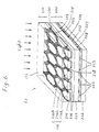
- Figure 7 shows the relationship between the shapes of conventional color filters and microlenses.
- the color filters 316R , 316G , and 316B are rectangular, so that white light or light of another color escapes from those parts protruding from the microlenses 314 . This reduces the display contrast or the mixing of colors lessens the clarity; therefore, it is desirable to make the shape of the color filters the same as that of the microlenses.
- both of the liquid crystal display panel and microlens array should be positioned near each other so that the microlenses in the microlens array individually correspond to the picture elements in the liquid crystal display panel. Moreover, when performing a display of color images, alignment is required between the color filter and the microlenses.
- An ultraviolet setting resin is usually used to combine optical parts such as achromatic composite lenses, various types of prisms, and deflecting beam splitters.
- cold-setting resins are sometimes used, they are not suited to mass production because of their long setting time.
- different kinds of glass are sometimes combined with each other, but there is little difference in their thermal expansion coefficients.
- liquid crystal display panels are required to have uniform electro-optical characteristics, the thickness of the panel should be constant.
- spacers are first spread out between the substrates, and thereafter, a liquid crystal is injected into the space between the substrates.
- spacers it is also necessary to use spacers in the sealing resin, although the sealing portions are not required to transmit light.
- thermosetting epoxy adhesives are usually used in view of the effects on the characteristics and reliability of the liquid crystal display device.
- the substrates to be combined with each other are usually made of the same material; therefore, it is not necessary to consider differences in thermal expansion coefficients.
- the microlens array converges the light, which would otherwise be incident upon the black matrix portion of the liquid crystal display panel, on the picture elements, so that the brightness of the display image is increased and the equivalent aperture ratio is raised.
- the microlens array should be combined uniformly with the liquid crystal display panel by adjusting the thickness of the adhesive therebetween so that the focal point of each of the microlenses is positioned in the area of the corresponding picture element.
- soda-lime glass containing a great amount of sodium ions is used as the substrate. Since soda-lime glass is not desirable as the substrate of liquid crystal display panels due to the elution of ions to the liquid crystal, which degrades the characteristics of the liquid crystal, borosilicate glass which has a low ion content is used.
- the preferred embodiments of the invention described herein provide (1) a compact, lightweight image display apparatus with significantly improved contrast and brightness of display images; (2) an image display apparatus in which the problems of light leakage and mixing of colored light are solved and the light passing through the microlens array and color filter is effectively utilized, thereby attaining further improved contrast and brightness of display images; and (3) an image display apparatus in which the substrate of the non-luminescent display panel and the microlens array are combined together without degrading the optical characteristics, and warp or separation does not readily occur and high thermal reliability is attained because the difference in thermal expansion coefficients is reduced.
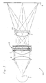
- Figure 1 is a schematic sectional view showing the configuration of an embodiment of a color image display apparatus of this invention.
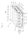
- Figure 2 is an enlarged perspective view showing a part of the display means in the image display apparatus of Figure 1.
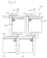
- Figure 3 is an enlarged plan view showing the neighborhood of the picture element electrodes in the liquid crystal display panel of the display means of Figure 2.
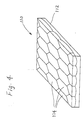
- Figure 4 is a schematic perspective view showing the microlens array of the display means of Figure 2, as illustrated from the light-outgoing side.
- Figure 5 is a schematic sectional view showing the configuration of another embodiment of a color image display apparatus of this invention.
- Figure 6 is an enlarged perspective view showing a part of the display means in the image display apparatus of Figure 5.
- Figure 7 is a schematic view showing the relationship between the shapes of the microlens and color filters in a conventional image display apparatus.
- FIG. 1 shows a color image display apparatus of this invention.
- This color image display apparatus 100 has a light source 2 and a reflecting mirror 3 .
- the light from the light source 2 and the reflecting mirror 3 passes through the condenser lenses 4 and 5 and then enters the display means 61 .
- the light source 2 is a white light source which can be a halogen lamp, metal halide lamp, or a xenon lamp.
- the reflecting mirror 3 reflects the light emitted by the light source 2 toward the opposite side and directs the light toward the display means 61 .
- Koehler illumination is used in this example, other illumination methods (e.g., critical illumination or telecentric illumination) can also be used.
- the light passing through the display means 61 is projected onto the screen 8 by the projection lens 7 , resulting in a color image.
- FIG. 2 is an enlarged perspective view showing a part of the display means 61 .
- the display means 61 has a microlens array 110 and a liquid crystal display panel 120 , both of which are combined with each other by means of an adhesive layer 130 made from a transparent material.
- the microlens array 110 is positioned on the light-incidence side of the display means 61 .
- the surface of the microlens array 110 toward the adhesive layer 130 has three primary-color (red, green, and blue) filters 116 (the respective colors of the filters are indicated by the numbers 116R , 116G , and 116B ) corresponding to each of the microlenses formed on the glass substrate 112 .
- three primary-color (red, green, and blue) filters 116 the respective colors of the filters are indicated by the numbers 116R , 116G , and 116B ) corresponding to each of the microlenses formed on the glass substrate 112 .
- the material used for the color filters 116 is preferably either an inorganic material or an organic material in consideration of resistance to light and heat.
- the inorganic material which can be used include an interference filter in which two kinds of oxide films with different refractive indices are alternately formed by electron beam deposition or sputtering.
- a specific example of an oxide film combination is titanium dioxide (TiO2) and silicon dioxide (SiO2).
- zirconium dioxide (ZrO2) can be used in place of TiO2
- magnesium fluoride (MgF2) can be used in place of SiO2.
- a known photolithographic process such as a lift-off technique or a photoetching technique can be used to pattern the interference color filter.
- organic pigment examples include a quinacridone red pigment, and phthalocyanine green and blue pigments. These organic pigments are dispersed uniformly in a photosensitive resin which serves as a binder and the predetermined pattern is formed from the mixture by a known photolithographic process.
- a shading mask 118 is provided between the color filters 116 .
- the shading mask 118 is not shown in Figure 1.
- the shading mask 118 is formed from a thin film of metal such as chrome, or a black pigment, by a known photolithographic process.
- the liquid crystal display panel 120 has the structure described below.
- the picture element electrodes 122 , driving signal lines 123 , switching elements (not shown), and scanning signal lines 124 are formed on the glass substrate 121 which is positioned on the light-incidence side.
- the opposite electrodes 127 are formed over the entire surface of the opposite glass substrate 126 so as to face the picture element electrodes 122 .
- the liquid crystal layer 128 is interposed between the glass substrates 121 and 126 .
- As the material used for the glass substrates 121 and 126 for example, borosilicate glass is used.
- the picture element electrodes 122 and opposite electrodes 127 are formed from a transparent conductive material such as indium tin oxide (ITO).
- the picture element electrodes 122 constitute the transmission areas, while the driving signal lines 123 , switching elements, scanning signal lines 124 , and the like constitute the shading areas which do not transmit light.
- FIG 3 shows an enlarged plan view showing the neighborhood of the picture element electrodes 122 which function as the display picture elements of the liquid crystal display panel 120 .
- This liquid crystal display panel 120 can be of the active matrix drive type.
- the picture element electrodes 122 are arranged in a matrix on the glass substrate 121 .
- the driving signals to these picture element electrodes 122 are supplied from the driving signal lines 123 via switching elements 125 such as thin-film transistors (TFTs).
- switching elements 125 such as thin-film transistors (TFTs).
- the microlens array 110 is made by injecting sodium ions, for example, into a glass substrate 112 made from soda-lime glass by a selective ion diffusion method or a ion-exchange method so that the glass substrate has an intensity distribution.
- the areas into which the sodium ions are injected are formed into convex microlenses 114 , for example, which have a larger refractive index than that of the glass substrate 112 .
- the microlens array 110 is obtained by arranging these kind of microlenses 114 in a matrix so that they individually correspond to the picture element electrodes 122 in the liquid crystal display panel 120 .
- the shape of the microlenses 114 is determined so that the light entering from the light source 2 through the condenser lenses 4 and 5 passes through each of the color filters 116 and then strikes the corresponding picture element electrodes 122 of the liquid crystal display panel 120 .
- the picture element electrodes 122 of the liquid crystal display panel 120 are formed in a delta-shaped matrix; therefore, the shapes of the microlenses 114 and the color filters 116 are both set to be hexagonal.
- Figure 4 is a schematic view showing only a part of the microlenses 114 in the microlens array 110 , as illustrated from the side of the adhesive layer 130 . This figure, however, does not show the color filters 116 or the shading mask 118 .
- the refractive index of each of the microlenses 114 becomes greater toward the center of the lens.
- each of the microlenses 114 is fused with the adjacent microlenses 114 at the borderline therebetween.
- the microlenses 114 and color filters 116 are aligned with the picture element electrodes 122 of the liquid crystal display panel 120 , the microlens array 110 is combined with the glass substrate 121 of the liquid crystal display panel 120 by means of an adhesive layer 130 made from a transparent material.
- the display means 61 is formed in a single unit.
- the transparent material which constitutes the adhesive layer 130 has a refractive index (1.4-1.6) near that of glass and a suitable viscosity (200-300 cps), as well as high adhesive strength.
- the transparent material which can be used include synthetic acrylic and epoxy resins such as AVR-100 of Threebond, UV-1003 of Sony Chemical, and NOA-61, 63, and 65 of Norland. Although these transparent materials are synthetic resins which can set under UV irradiation, thermosetting resins can also be used.
- the thickness of the adhesive layer 124 should be from 10 to 100 microns since separation will readily occur if less than 10 microns and too much time is required for setting if greater than 100 microns. For example, if the adhesive layer 130 is approximately 100 microns thick, it will set sufficiently in 20 seconds when irradiated by a 250-W high-pressure mercury lamp from a height of 6 cm.
- the thickness of the adhesive layer 130 is maintained uniform by mixing an appropriate amount of spacers 132 in the transparent material.
- the spacers 132 are not shown in Figure 1.
- the spacers 132 are spherical plastic particles in the normal state.
- the diameter of the spacers 132 is preferably from 10 to 100 microns, and their index of refraction is preferably from 1.4 to 1.6.
- Spacers 132 are selected which have an expandability and an elastic coefficient lower than that of the transparent material.
- the mixing ratio of spacers 132 to transparent material is, for example, several to one square millimeter of the adhesive layer 130 .
- the materials used for spacers 132 can be styrene or acrylic synthetic resins such as Micropearl SP of Sekisui Fine Chemicals and Epostar CP of Nihon Shokubai.
- the light which is emitted from the light source 2 and is incident upon the display means 61 via the condenser lenses 4 and 5 is converged on each of the picture element electrodes 122 of the liquid crystal display panel 120 by the microlens array 110 , and when passing through the liquid crystal layer 128 , the light undergoes intensity modulation corresponding to the driving signal. After passing through the liquid crystal display panel 120 , this modulated light is diffused within a circular cone corresponding to a solid angle determined by the aperture ratio established for the microlenses 114 .
- the aperture D1 of the projection lens 7 is selected so that such a bundle of rays from any microlens 114 can be received. By this means, the light passing through the liquid crystal display panel 120 (i.e., display image) is not restricted by the projection lens 7 .
- the display image enlarged by the projection lens 7 is projected on the screen 8 .
- image display apparatuses can be made more compact and lightweight, as compared with conventional image display apparatuses using three liquid crystal display panels corresponding to the three primary colors (i.e., red, green, and blue).
- FIG. 5 shows another color image display apparatus of this invention.
- This color image display apparatus 200 is the same as that obtained in Example 1, except for the structure of the microlens array of the display means 62 .
- the materials used for each part and the method for producing the image display apparatus are the same as those used in Example 1.
- FIG. 6 is an enlarged perspective view showing a part of the display means 62 .
- the display means 62 has a microlens array 210 and a liquid crystal display panel 220 , both of which are combined with each other by means of an adhesive layer 230 made from a transparent material.
- the microlens array 210 is positioned on the light-incidence side of the display means 62 .
- the microlens array 210 of this example differs from that used in Example 1 in that the positional relationship of the microlens and color filter is reversed with respect to the direction of light incidence.
- the surface of the microlens array 210 toward the adhesive layer 230 has microlenses 214 corresponding to the three primary-color (red, green, and blue) filters 216 (the respective colors of the filters are indicated by the numbers 216R , 216G , and 216B ) formed on the glass substrate 212 .
- a shading mask 218 is also provided between the color filters 216 .
- the shading mask 218 is not shown in Figure 5.
- the liquid crystal display panel 220 has the same structure as that of the liquid crystal display panel 120 used in Example 1.
- the picture element electrodes 222 , driving signal lines 223 , switching elements (not shown), and scanning signal lines 224 are formed on the glass substrate 221 positioned on the light-incidence side.
- the opposite electrodes 227 are formed over the entire surface of the opposite glass substrate 226 so as to face the picture element electrodes 222 .
- the liquid crystal layer 228 is disposed between the glass substrates 221 and 226 .
- the picture element electrodes 222 constitute the transmission areas, while the driving signal lines 223 , switching elements, and scanning signal lines 224 constitute the shading areas which do not transmit light.
- the display means 62 is produced as follows. First, color filters 216 are formed on the glass substrate 212 in the predetermined pattern of the three primary colors (i.e., red, green, and blue) so that the color filters 216 individually correspond to the picture element electrodes 222 of the liquid crystal display panel 220 . These color filters 216 are formed by applying a synthetic resin containing pigment dispersed therein, or by selectively depositing an interference filter through sputtering, which contains a plurality of oxide films with different refractive indices.
- a transparent resin layer 219 is then formed on the glass substrate 212 with the color filters 216 , and after the surface is flattened, the substrate 212 is baked.
- a thermoplastic resin with a relatively high refractive index is selectively applied to the surface of the transparent resin layer 219 corresponding to the positions of the color filters 216 , and then the thermoplastic resin is heated to a temperature above its softening point to form the convex lenses.
- the microlens array 210 is obtained by arranging the microlenses 214 in a matrix so that the microlenses 214 individually correspond to the picture element electrodes 222 in the liquid crystal display panel 220 .
- the shape of the microlenses 214 is determined so that the light entering from the light source 2 through the condenser lenses 4 and 5 passes through each of the color filters 216 and then strikes the picture element electrodes 222 of the liquid crystal display panel 220 .
- the picture element electrodes 222 of the liquid crystal display panel 220 are formed in a delta-shaped matrix; therefore, the shapes of the microlenses 214 and the color filters 216 are both set to be hexagonal.
- the microlens array 210 the light incident upon the color filters 216 can also be effectively converged on the picture element electrodes 222 of the liquid crystal display panel 220 .
- the microlens array 210 is combined with the glass substrate 221 of the liquid crystal display panel 220 by means of an adhesive layer 230 made from a transparent material.
- the display means 62 is formed in a single unit. In this example, it is not necessary to mix any spacers in the adhesive layer 230 .
- the light which is emitted from the light source 2 and is incident upon the display means 62 via the condenser lenses 4 and 5 is colored by each color filter 216 of the microlens array 210 and converged on each of the picture element electrodes 222 of the liquid crystal display panel 220 by each microlens 214 .
- the light undergoes intensity modulation corresponding to the driving signal.
- this modulated light is diffused within a circular cone corresponding to a solid angle determined by the aperture ratio established for the microlenses 214 .
- the aperture D1 of the projection lens 7 is selected so that such a bundle of rays from any microlens 214 can be received.
- the light passing through the liquid crystal display panel 220 i.e., display image
- the display image enlarged by the projection lens 7 is projected on the screen 8 .
- image display apparatuses can be made more compact and lightweight, as compared with conventional image display apparatuses using three liquid crystal display panels corresponding to the three primary colors (i.e., red, green, and blue).
- liquid crystal display panels were used as the non-luminescent display panels, other non-luminescent display panels such as electrochromic display panels or transmissive-type ceramic display panels can also be used.
- each of the microlenses in the microlens array can be selected so as to correspond to the picture element matrix in the non-luminescent display panel; that is, it may be circular, rectangular, hexagonal, or may have any other polygonal shape.
- the shape of the color filters should preferably be the same as that of the microlenses.
Priority Applications (1)
| Application Number | Priority Date | Filing Date | Title |
|---|---|---|---|
| EP94203513A EP0644450B1 (en) | 1989-07-19 | 1990-07-19 | Image display apparatus |
Applications Claiming Priority (8)
| Application Number | Priority Date | Filing Date | Title |
|---|---|---|---|
| JP187715/89 | 1989-07-19 | ||
| JP1187715A JP2522549B2 (ja) | 1989-07-19 | 1989-07-19 | 貼り合わせ構造 |
| JP1199723A JPH0363626A (ja) | 1989-07-31 | 1989-07-31 | 投影型カラー液晶表示装置 |
| JP199723/89 | 1989-07-31 | ||
| JP32653889A JP2677436B2 (ja) | 1989-12-15 | 1989-12-15 | カラー画像表示装置 |
| JP1326536A JP2677435B2 (ja) | 1989-12-15 | 1989-12-15 | カラー画像表示装置 |
| JP326538/89 | 1989-12-15 | ||
| JP326536/89 | 1989-12-15 |
Related Child Applications (2)
| Application Number | Title | Priority Date | Filing Date |
|---|---|---|---|
| EP94203513.0 Division-Into | 1990-07-19 | ||
| EP94203513A Division EP0644450B1 (en) | 1989-07-19 | 1990-07-19 | Image display apparatus |
Publications (3)
| Publication Number | Publication Date |
|---|---|
| EP0409618A2 EP0409618A2 (en) | 1991-01-23 |
| EP0409618A3 EP0409618A3 (en) | 1991-09-18 |
| EP0409618B1 true EP0409618B1 (en) | 1995-09-20 |
Family
ID=27475340
Family Applications (2)
| Application Number | Title | Priority Date | Filing Date |
|---|---|---|---|
| EP94203513A Expired - Lifetime EP0644450B1 (en) | 1989-07-19 | 1990-07-19 | Image display apparatus |
| EP90307902A Expired - Lifetime EP0409618B1 (en) | 1989-07-19 | 1990-07-19 | An image display apparatus |
Family Applications Before (1)
| Application Number | Title | Priority Date | Filing Date |
|---|---|---|---|
| EP94203513A Expired - Lifetime EP0644450B1 (en) | 1989-07-19 | 1990-07-19 | Image display apparatus |
Country Status (5)
| Country | Link |
|---|---|
| US (2) | US5381187A (es) |
| EP (2) | EP0644450B1 (es) |
| KR (1) | KR940000590B1 (es) |
| DE (2) | DE69022504T2 (es) |
| ES (2) | ES2077648T3 (es) |
Families Citing this family (43)
| Publication number | Priority date | Publication date | Assignee | Title |
|---|---|---|---|---|
| ES2077648T3 (es) * | 1989-07-19 | 1995-12-01 | Sharp Kk | Aparato de presentacion de imagen. |
| WO1992016872A1 (fr) * | 1991-03-20 | 1992-10-01 | Mitsubishi Denki Kabushiki Kaisha | Dispositif d'affichage du type a projection |
| KR960011399B1 (ko) * | 1991-04-03 | 1996-08-22 | 샤프 가부시끼가이샤 | 광학 소자 조립 장치 |
| JP2760915B2 (ja) * | 1991-06-03 | 1998-06-04 | 日本板硝子株式会社 | 画像表示装置 |
| KR940009137B1 (ko) * | 1992-02-14 | 1994-10-01 | 삼성전자 주식회사 | 액정표시판 및 그 제조방법 |
| US5581379A (en) * | 1993-02-15 | 1996-12-03 | Omron Corporation | Rectangular based convex microlenses surrounded within a frame and method of making |
| US5617152A (en) * | 1993-06-20 | 1997-04-01 | Unic View Ltd. | Projector system for video and computer generated information |
| US5706062A (en) * | 1993-06-20 | 1998-01-06 | Unic View Ltd. | Projector system including keystone correction |
| CA2167591A1 (en) * | 1993-06-29 | 1995-01-12 | Ronald C. Robinder | Color liquid crystal display |
| JPH0798339A (ja) * | 1993-09-28 | 1995-04-11 | Yutaka Denki Seisakusho:Kk | 電流検出パターン |
| JPH07225303A (ja) * | 1993-12-16 | 1995-08-22 | Sharp Corp | マイクロレンズ基板及びそれを用いた液晶表示素子ならびに液晶プロジェクタ装置 |
| FI97264C (fi) * | 1994-10-28 | 1996-11-11 | Tvi Temet Vision Ind Oy | Menetelmä valoilmaisinrivin asemoimiseksi ja valojako- ja ilmaisinrakenne viivakameraa varten |
| US5606436A (en) * | 1994-11-21 | 1997-02-25 | Proxima Corporation | Liquid crystal projection panel construction and method of making same |
| JPH08179300A (ja) * | 1994-12-22 | 1996-07-12 | Sony Corp | カラー表示装置 |
| JP3251150B2 (ja) * | 1994-12-29 | 2002-01-28 | 日本板硝子株式会社 | 平板マイクロレンズアレイおよびその製造方法 |
| US5836096A (en) * | 1996-03-04 | 1998-11-17 | Brauer; William R. | Apparatus for illuminating medical diagnostic imaging film with enhanced viewability |
| IT1285368B1 (it) * | 1996-05-27 | 1998-06-03 | Fiat Ricerche | Dispositivo a microfiltri e microchopper per la selezione dinamica di colori ed immagini. |
| US5992758A (en) * | 1996-09-23 | 1999-11-30 | Agro-Mack Enterprises Ltd. | Proximity detector for ground-based implements |
| JPH10254370A (ja) * | 1997-03-10 | 1998-09-25 | Canon Inc | 表示パネル及びそれを用いた投射型表示装置 |
| JP3750303B2 (ja) * | 1997-09-11 | 2006-03-01 | ソニー株式会社 | 液晶表示装置 |
| US6327011B2 (en) | 1997-10-20 | 2001-12-04 | Lg Electronics, Inc. | Liquid crystal display device having thin glass substrate on which protective layer formed and method of making the same |
| US6078371A (en) * | 1998-10-05 | 2000-06-20 | Canon Kabushiki Kaisha | Liquid crystal device and liquid crystal display apparatus |
| JP2001110801A (ja) * | 1999-10-05 | 2001-04-20 | Takeshi Yao | パターン形成方法、並びに電子素子、光学素子及び回路基板 |
| JP2001188107A (ja) * | 1999-12-28 | 2001-07-10 | Seiko Epson Corp | マイクロレンズ基板の製造方法、マイクロレンズ基板、液晶パネル用対向基板、液晶パネルおよび投射型表示装置 |
| US6835535B2 (en) | 2000-07-31 | 2004-12-28 | Corning Incorporated | Microlens arrays having high focusing efficiency |
| WO2002010804A1 (en) | 2000-07-31 | 2002-02-07 | Rochester Photonics Corporation | Structure screens for controlled spreading of light |
| US7092165B2 (en) * | 2000-07-31 | 2006-08-15 | Corning Incorporated | Microlens arrays having high focusing efficiency |
| JP2002182008A (ja) * | 2000-10-04 | 2002-06-26 | Sharp Corp | 光学レンズシステム、画像表示装置、マイクロレンズアレイ、液晶表示素子および投影型液晶表示装置 |
| US6970288B2 (en) * | 2001-06-01 | 2005-11-29 | Toppan Printing Co., Ltd. | Micro-lens sheet and projection screen |
| TW520616B (en) * | 2001-12-31 | 2003-02-11 | Ritdisplay Corp | Manufacturing method of organic surface light emitting device |
| DE10245104B4 (de) * | 2002-09-27 | 2008-08-07 | Carl Zeiss Jena Gmbh | Projektionsanordnung und Projektionsverfahren |
| US7414595B1 (en) | 2003-12-07 | 2008-08-19 | Advanced Simulation Displays Co. | Virtual mosaic wide field of view display system |
| TW200710018A (en) * | 2005-08-30 | 2007-03-16 | Hitachi Maxell | Microlens array substrate and method of manufacturing microlens array substrate |
| JP5220015B2 (ja) * | 2007-08-01 | 2013-06-26 | シャープ株式会社 | 液晶表示装置及びその製造方法 |
| WO2009098621A1 (en) * | 2008-02-08 | 2009-08-13 | Koninklijke Philips Electronics N.V. | Light module device |
| JP2015179145A (ja) * | 2014-03-19 | 2015-10-08 | 株式会社東芝 | 液晶光学素子及び画像装置 |
| US9977152B2 (en) | 2016-02-24 | 2018-05-22 | Hong Kong Beida Jade Bird Display Limited | Display panels with integrated micro lens array |
| US10304375B2 (en) | 2016-09-23 | 2019-05-28 | Hong Kong Beida Jade Bird Display Limited | Micro display panels with integrated micro-reflectors |
| JP7151255B2 (ja) * | 2018-08-06 | 2022-10-12 | セイコーエプソン株式会社 | 虚像表示装置 |
| US11114483B2 (en) * | 2018-08-10 | 2021-09-07 | Omnivision Technologies, Inc. | Cavityless chip-scale image-sensor package |
| CN109817120B (zh) * | 2019-02-14 | 2020-06-30 | 宁波财经学院 | 一种数字互动景观系统 |
| KR20210106606A (ko) * | 2020-02-20 | 2021-08-31 | 삼성디스플레이 주식회사 | 표시 장치 |
| CN112596332B (zh) * | 2020-12-23 | 2022-03-11 | 广景视睿科技(深圳)有限公司 | 一种投影系统及投影仪 |
Family Cites Families (23)
| Publication number | Priority date | Publication date | Assignee | Title |
|---|---|---|---|---|
| DE2912467A1 (de) * | 1979-03-29 | 1980-10-09 | Siemens Ag | Fluessigkristallanzeige |
| JPH0756547B2 (ja) * | 1984-02-08 | 1995-06-14 | 日本電気株式会社 | 透過型表示素子 |
| JPS60165624A (ja) * | 1984-02-08 | 1985-08-28 | Nec Corp | 透過型表示素子 |
| JPS60165622A (ja) * | 1984-02-08 | 1985-08-28 | Nec Corp | 透過型表示素子 |
| JPS60165621A (ja) * | 1984-02-08 | 1985-08-28 | Nec Corp | 透過型表示素子 |
| JPS60262131A (ja) * | 1984-06-08 | 1985-12-25 | Sharp Corp | 液晶表示装置 |
| JPS6111788A (ja) * | 1984-06-26 | 1986-01-20 | カシオ計算機株式会社 | 画像表示装置 |
| US4715686A (en) * | 1984-11-16 | 1987-12-29 | Seiko Epson Corporation | Light-passive display device and method of manufacturing same |
| JPS61208080A (ja) * | 1985-03-11 | 1986-09-16 | 三菱電機株式会社 | 液晶カラ−イメ−ジ表示装置 |
| JPS61284731A (ja) * | 1985-06-11 | 1986-12-15 | Seiko Epson Corp | 透過型液晶表示装置 |
| JP2754529B2 (ja) * | 1985-10-22 | 1998-05-20 | セイコーエプソン株式会社 | 液晶装置 |
| JPS62203126A (ja) * | 1986-03-04 | 1987-09-07 | Matsushita Electric Ind Co Ltd | 表示装置 |
| JPH0762745B2 (ja) * | 1986-05-15 | 1995-07-05 | 大日本印刷株式会社 | 多色電気光学表示装置用電極基板 |
| JPS62267791A (ja) * | 1986-05-15 | 1987-11-20 | 大日本印刷株式会社 | 多色電気光学表示装置用電極基板 |
| JPS6344624A (ja) * | 1986-08-12 | 1988-02-25 | Fuji Photo Film Co Ltd | 液晶デバイス |
| JPS63124028A (ja) * | 1986-11-13 | 1988-05-27 | Fuji Photo Film Co Ltd | 液晶シヤツタアレイ |
| JPS6435416A (en) * | 1987-07-30 | 1989-02-06 | Matsushita Electric Ind Co Ltd | Liquid crystal panel |
| JP2566417B2 (ja) * | 1987-08-05 | 1996-12-25 | 旭光学工業株式会社 | 焦点板 |
| JPH0769532B2 (ja) * | 1988-06-11 | 1995-07-31 | シャープ株式会社 | 投影型表示装置 |
| JPH0769533B2 (ja) * | 1988-06-30 | 1995-07-31 | シャープ株式会社 | 液晶表示装置 |
| JPH0642126B2 (ja) * | 1988-10-26 | 1994-06-01 | シャープ株式会社 | 投影型画像表示装置 |
| JP2815910B2 (ja) * | 1989-07-19 | 1998-10-27 | シャープ株式会社 | 投影形画像表示装置 |
| ES2077648T3 (es) * | 1989-07-19 | 1995-12-01 | Sharp Kk | Aparato de presentacion de imagen. |
-
1990
- 1990-07-19 ES ES90307902T patent/ES2077648T3/es not_active Expired - Lifetime
- 1990-07-19 EP EP94203513A patent/EP0644450B1/en not_active Expired - Lifetime
- 1990-07-19 ES ES94203513T patent/ES2122151T3/es not_active Expired - Lifetime
- 1990-07-19 DE DE69022504T patent/DE69022504T2/de not_active Expired - Fee Related
- 1990-07-19 KR KR1019900010989A patent/KR940000590B1/ko not_active IP Right Cessation
- 1990-07-19 DE DE69032668T patent/DE69032668T2/de not_active Expired - Lifetime
- 1990-07-19 EP EP90307902A patent/EP0409618B1/en not_active Expired - Lifetime
-
1992
- 1992-02-13 US US07/833,612 patent/US5381187A/en not_active Expired - Lifetime
-
1994
- 1994-10-07 US US08/319,720 patent/US5715022A/en not_active Expired - Lifetime
Also Published As
| Publication number | Publication date |
|---|---|
| DE69022504T2 (de) | 1996-03-28 |
| US5715022A (en) | 1998-02-03 |
| KR910003554A (ko) | 1991-02-27 |
| EP0409618A3 (en) | 1991-09-18 |
| EP0644450B1 (en) | 1998-09-16 |
| DE69022504D1 (de) | 1995-10-26 |
| EP0644450A1 (en) | 1995-03-22 |
| ES2122151T3 (es) | 1998-12-16 |
| DE69032668T2 (de) | 1999-04-08 |
| ES2077648T3 (es) | 1995-12-01 |
| US5381187A (en) | 1995-01-10 |
| EP0409618A2 (en) | 1991-01-23 |
| DE69032668D1 (de) | 1998-10-22 |
| KR940000590B1 (ko) | 1994-01-26 |
Similar Documents
| Publication | Publication Date | Title |
|---|---|---|
| EP0409618B1 (en) | An image display apparatus | |
| US5056912A (en) | Projection type image display apparatus | |
| JP3957986B2 (ja) | 反射型表示装置 | |
| TW482919B (en) | Projection type color image display apparatus | |
| EP1701202B1 (en) | Method of producing micro-lens-carrying display panel and display device | |
| KR100189278B1 (ko) | 투영형 칼라 표시 장치 | |
| JPH08297286A (ja) | 液晶表示装置 | |
| JP2000056296A (ja) | 液晶表示装置 | |
| JPH03140920A (ja) | 投写型表示装置及び該投写型表示装置に用いる液晶表示装置 | |
| JP2849492B2 (ja) | 投影型液晶表示装置 | |
| US5274480A (en) | Projection type display apparatus having an aperture stop means including non-circular openings | |
| JP4096346B2 (ja) | 光変調素子および画像投射表示装置 | |
| EP0699937B1 (en) | Method of compensating for a luminance point defect in transmission display device and correspondingly componsentated display element | |
| CN101017275B (zh) | 聚光基板、电光装置、电光装置用基板、投影机以及电子设备 | |
| JPH0430140A (ja) | 投影型カラー液晶表示装置 | |
| JP2000338476A (ja) | 反射型液晶表示装置用カラーフィルター基板 | |
| JPH049922A (ja) | 投影型カラー液晶表示装置 | |
| JPH112718A (ja) | カラーフィルタおよびカラー液晶表示装置 | |
| JPH0363626A (ja) | 投影型カラー液晶表示装置 | |
| JPH09304762A (ja) | カラー液晶表示装置およびその製造方法 | |
| JP2677436B2 (ja) | カラー画像表示装置 | |
| JPH07261164A (ja) | 液晶表示装置用基板 | |
| JP2972079B2 (ja) | 投影型画像表示装置 | |
| JPH03113427A (ja) | 単純マトリックス型液晶表示装置 | |
| JPH03187592A (ja) | カラー画像表示装置 |
Legal Events
| Date | Code | Title | Description |
|---|---|---|---|
| PUAI | Public reference made under article 153(3) epc to a published international application that has entered the european phase |
Free format text: ORIGINAL CODE: 0009012 |
|
| AK | Designated contracting states |
Kind code of ref document: A2 Designated state(s): DE ES FR GB NL |
|
| 17P | Request for examination filed |
Effective date: 19901228 |
|
| PUAL | Search report despatched |
Free format text: ORIGINAL CODE: 0009013 |
|
| AK | Designated contracting states |
Kind code of ref document: A3 Designated state(s): DE ES FR GB NL |
|
| 17Q | First examination report despatched |
Effective date: 19930809 |
|
| GRAA | (expected) grant |
Free format text: ORIGINAL CODE: 0009210 |
|
| AK | Designated contracting states |
Kind code of ref document: B1 Designated state(s): DE ES FR GB NL |
|
| XX | Miscellaneous (additional remarks) |
Free format text: TEILANMELDUNG 94203513.0 EINGEREICHT AM 19/07/90. |
|
| REF | Corresponds to: |
Ref document number: 69022504 Country of ref document: DE Date of ref document: 19951026 |
|
| ET | Fr: translation filed | ||
| REG | Reference to a national code |
Ref country code: ES Ref legal event code: FG2A Ref document number: 2077648 Country of ref document: ES Kind code of ref document: T3 |
|
| PLBE | No opposition filed within time limit |
Free format text: ORIGINAL CODE: 0009261 |
|
| STAA | Information on the status of an ep patent application or granted ep patent |
Free format text: STATUS: NO OPPOSITION FILED WITHIN TIME LIMIT |
|
| 26N | No opposition filed | ||
| PGFP | Annual fee paid to national office [announced via postgrant information from national office to epo] |
Ref country code: DE Payment date: 20010709 Year of fee payment: 12 |
|
| PGFP | Annual fee paid to national office [announced via postgrant information from national office to epo] |
Ref country code: FR Payment date: 20010712 Year of fee payment: 12 |
|
| PGFP | Annual fee paid to national office [announced via postgrant information from national office to epo] |
Ref country code: GB Payment date: 20010718 Year of fee payment: 12 |
|
| PGFP | Annual fee paid to national office [announced via postgrant information from national office to epo] |
Ref country code: ES Payment date: 20010719 Year of fee payment: 12 |
|
| PGFP | Annual fee paid to national office [announced via postgrant information from national office to epo] |
Ref country code: NL Payment date: 20010730 Year of fee payment: 12 |
|
| REG | Reference to a national code |
Ref country code: GB Ref legal event code: IF02 |
|
| PG25 | Lapsed in a contracting state [announced via postgrant information from national office to epo] |
Ref country code: GB Free format text: LAPSE BECAUSE OF NON-PAYMENT OF DUE FEES Effective date: 20020719 |
|
| PG25 | Lapsed in a contracting state [announced via postgrant information from national office to epo] |
Ref country code: ES Free format text: LAPSE BECAUSE OF NON-PAYMENT OF DUE FEES Effective date: 20020720 |
|
| PG25 | Lapsed in a contracting state [announced via postgrant information from national office to epo] |
Ref country code: NL Free format text: LAPSE BECAUSE OF NON-PAYMENT OF DUE FEES Effective date: 20030201 Ref country code: DE Free format text: LAPSE BECAUSE OF NON-PAYMENT OF DUE FEES Effective date: 20030201 |
|
| GBPC | Gb: european patent ceased through non-payment of renewal fee |
Effective date: 20020719 |
|
| PG25 | Lapsed in a contracting state [announced via postgrant information from national office to epo] |
Ref country code: FR Free format text: LAPSE BECAUSE OF NON-PAYMENT OF DUE FEES Effective date: 20030331 |
|
| NLV4 | Nl: lapsed or anulled due to non-payment of the annual fee |
Effective date: 20030201 |
|
| REG | Reference to a national code |
Ref country code: FR Ref legal event code: ST |
|
| REG | Reference to a national code |
Ref country code: ES Ref legal event code: FD2A Effective date: 20030811 |