EP0405564A2 - Quantendraht-Feldeffekttransistor - Google Patents
Quantendraht-Feldeffekttransistor Download PDFInfo
- Publication number
- EP0405564A2 EP0405564A2 EP90112377A EP90112377A EP0405564A2 EP 0405564 A2 EP0405564 A2 EP 0405564A2 EP 90112377 A EP90112377 A EP 90112377A EP 90112377 A EP90112377 A EP 90112377A EP 0405564 A2 EP0405564 A2 EP 0405564A2
- Authority
- EP
- European Patent Office
- Prior art keywords
- semiconductor layer
- layer
- effect transistor
- semi
- field effect
- Prior art date
- Legal status (The legal status is an assumption and is not a legal conclusion. Google has not performed a legal analysis and makes no representation as to the accuracy of the status listed.)
- Granted
Links
Images

Classifications
-
- B—PERFORMING OPERATIONS; TRANSPORTING
- B82—NANOTECHNOLOGY
- B82Y—SPECIFIC USES OR APPLICATIONS OF NANOSTRUCTURES; MEASUREMENT OR ANALYSIS OF NANOSTRUCTURES; MANUFACTURE OR TREATMENT OF NANOSTRUCTURES
- B82Y10/00—Nanotechnology for information processing, storage or transmission, e.g. quantum computing or single electron logic
-
- H—ELECTRICITY
- H10—SEMICONDUCTOR DEVICES; ELECTRIC SOLID-STATE DEVICES NOT OTHERWISE PROVIDED FOR
- H10D—INORGANIC ELECTRIC SEMICONDUCTOR DEVICES
- H10D30/00—Field-effect transistors [FET]
- H10D30/01—Manufacture or treatment
- H10D30/014—Manufacture or treatment of FETs having zero-dimensional [0D] or one-dimensional [1D] channels, e.g. quantum wire FETs, single-electron transistors [SET] or Coulomb blockade transistors
-
- H—ELECTRICITY
- H10—SEMICONDUCTOR DEVICES; ELECTRIC SOLID-STATE DEVICES NOT OTHERWISE PROVIDED FOR
- H10D—INORGANIC ELECTRIC SEMICONDUCTOR DEVICES
- H10D30/00—Field-effect transistors [FET]
- H10D30/40—FETs having zero-dimensional [0D], one-dimensional [1D] or two-dimensional [2D] charge carrier gas channels
- H10D30/43—FETs having zero-dimensional [0D], one-dimensional [1D] or two-dimensional [2D] charge carrier gas channels having 1D charge carrier gas channels, e.g. quantum wire FETs or transistors having 1D quantum-confined channels
-
- H—ELECTRICITY
- H10—SEMICONDUCTOR DEVICES; ELECTRIC SOLID-STATE DEVICES NOT OTHERWISE PROVIDED FOR
- H10D—INORGANIC ELECTRIC SEMICONDUCTOR DEVICES
- H10D62/00—Semiconductor bodies, or regions thereof, of devices having potential barriers
- H10D62/80—Semiconductor bodies, or regions thereof, of devices having potential barriers characterised by the materials
- H10D62/85—Semiconductor bodies, or regions thereof, of devices having potential barriers characterised by the materials being Group III-V materials, e.g. GaAs
Definitions
- the present invention relates to a field effect transistor (referred to as an FET hereinafter) using a compound semiconductor, and more particularly to an FET employing a quasi one-dimensional electron gas regime that is generated in the selectively doped heterojunction interfaces of a striped channel structure.
- an FET field effect transistor
- a two-dimensional electron gas field effect transistor which utilizes the excellent carrier transport characteristic of two-dimensional electron gas generated in the selectively doped heterojunction interfaces is expected to become available as a low noise element or a large power element for the ultrahigh frequency band and a fundamental element for very high speed digital integrated circuits.
- a quasi one-dimensional electron gas FET which is aimed at further enhancing the performance of a two-dimensional electron gas FET by restricting the direction of the motion of its two-dimensional electron gas to only one direction of from the source to the drain.
- a quasi one-dimensional electron gas FET one may mention the type in which a part of the two-dimensional electron gas is depleted by the application of a gate bias across striped N type cap layers.
- the field effect transistor in accordance with the present invention includes a semi-insulating semiconductor substrate, a plurality of laminated structures, each consisting of a first semiconductor layer, a second semiconductor layer having an electron affinity layer than that of the first semiconductor layer and a third semiconductor layer having an electron affinity which is substantially the same as that of the first semiconductor layer, formed in stripe shape on the substrate, a gate electrode which traverses uninterruptedly the portions of the surface of the semi-insulating semiconductor substrate exposed between the plurality of the striped laminated structures and both of the side faces and the upper faces of the plurality of the striped laminated structures, and extends in the direction intersecting the lengthwise direction of the stripes, and a source electrode and a drain electrode which commonly connect the respective ends in the lengthwise direction of the striped laminated structures with the gate electrode in between.
- the field effect transistor of the present invention it is possible to control the quasi one-dimensional electron gases that are generated in the interfaces of the second semiconductor layers of the selectively doped heterojunctions not only with a gate electric field pointed toward the substrate but also with gate electric fields pointed to sideways from both side faces of the striped layers. In other words, it is possible to suppress the two-dimensional motion of the electron gas.
- the first semiconductor layer between the electron gas and the substrate acts as a potential barrier layer so that it is possible to suppress the divergence of the quasi one-dimensional electron gas in the direction toward the substrate, whereby restricting the three-dimensional motion of the electron gas.
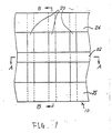
- the quasi one-dimensional electron gas FET 10 includes a plurality of multilayered stripes 20 provided on the surface of a semi-insulating GaAs substrate 11.
- Each of the stripes 20 consists from the bottom upward an N type AlGaAs layer 12, an undoped GaAs layer 14 and an N type AlGaAs layer 18, where the lower layer 14 and the upper layer 18 serves electron supplying layers, and the intermediate layer 14 serves as a channel layer.
- the intermediate layer 14 serves as a channel layer.
- the lower layer 18 serves also as a potential barrier layer.
- a source electrode 24 is provided on one of the end portions in the lengthwise direction of the stripes 20, connecting one end of each of the stripes 20 in common while a drain electrode 25 is provided placed commonly on the other ends of the stripes 20.
- These electrodes have a constitution in which a gold-germanium (AuGe) layer is overlaid with a nickel (Ni) layer.
- a gate electrode 22 which runs in the direction perpendicular to the lengthwise direction of the stripes 20.
- the gate electrode 22 which has a constitution in which a Ti layer is overlaid with an Al layer covers uninterruptedly the portions of the surface of the substrate 11 exposed between the stripes 20, one of the side faces, the upper surface and the other side face of the respective stripes 20.
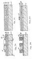
- FIGS. 2a to 5a and FIGS. 2b to 5b the method of fabrication of the FET in FIG. 1 will be described.
- a 100 nm-thick N type AlGaAs layer (lower layer) 12 doped with silicon to a concentration of about 2 x 1018 cm ⁇ 3, a 60 nm-thick undoped GaAs layer (intermediate layer) and a 30 nm-thick N type AlGaAs layer (upper layer) doped with silicon to a concentration of about 2 x 1018 cm ⁇ 3 are sequentially deposited epitaxially on a semi-insulating GaAs substrate 11 by means a molecular beam epitaxy (MBE) or a metal organic chemical vapor deposition (MOCVD).
- MBE molecular beam epitaxy
- MOCVD metal organic chemical vapor deposition
- resist 21 is formed on the portions intended for the stripes by means a direct writing electron beam lithography.
- the width of the resist 21 in the intended portions for the stripes is set to be about 0.3 ⁇ m, and the ratio of the stripe width to the space between the stripes is set to be 1 : 2.
- stripe layers 20 are formed as shown in FIGS. 3a and 3b by selectively etching the upper layer N type AlGaAs layer 18, the undoped GaAs layer 14 and the lower layer N type AlGaAs layer 12 by means of a wet etching that uses phosphoric acid (H3PO4) solution or a dry etching that uses chlorine (Cl2) gas, with the resist 21 as the mask.
- H3PO4 phosphoric acid
- Cl2 chlorine
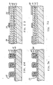
- resist 31 is formed on the portions other than those intended for the source and the drain electrodes, then a layer 23 is formed by sequentially evaporating a gold-germanium alloy layer and a nickel layer.
- a source electrode 24 and a drain electrode 25 consisting of gold-germanium and nickel are formed by a lift-off process which removes unwanted gold-germanium and nickel along with the resist 31, completing an element part by subjecting it to a heat treatment at 420°C.
- a quasi one-dimensional electron gas FET which can control the quasi one-dimensional electron gases 15 and 16 that are generated in the interfaces of the selectively doped heterojunctions on the stripes not only by a gate electric field that is directed from the surface toward the substrate but also by the gate electric fields which are pointed from both side faces of the stripe structures 20 to the sideways. Consequently, the lateral divergence of these quasi one-dimensional electron gases 15 and 16 can be suppresed even when the accelerating electric field in the direction of stripes becomes high.
- the divergence of the quasi one-dimensional electron gases 15 and 16 it can be suppressed to a minimum since there is provided a potential barrier layer 12 with a large band gap energy between the channel layer 14 and the semi-insulating substrate 11. Consequently, it is possible to maintain a one-dimensional electron conduction even in the operation under high electric fields which enables to obtain an FET with high current gain cut-off frequency under a wide range of bias conditions.
- electrons are supplied to the channel layer 14 by two of the upper and lower electron supplying layers 18 and 12 that sandwiches the channel layer 14, so that it becomes possible to realize a high current operation.
- the depletion layer due to the application of a gate voltage not only extends in the direction from the gate side to the substrate but also extends from both side faces of the stripe structures 20 so as to wrap the stripe structures, so that an improved control of the conduction electron flow for the same changes in the gate voltage, whereby making it possible to obtain a large value for the transconductance.
- the FET in accordance with the present invention can be fabricated by a relatively simple process, and can be applied to a wide range of field from low noise elements in the ultrahigh frequency band to fundamental elements for very high speed digital integrated circuits,
- the gate electrode 22 and the source and the drain electrodes 24 and 25 are formed on the N type AlGaAs electron supplying layer 18 in the upper layer in direct contact with it.
- an N type AlGaAs layer is used as the material for the lower layer 12 of the stripe structure 20.
- it may be replaced by a high resistance AlGaAs layer or a P type AlGaAs layer.
- a P type AlGaAs potential barrier layer 13 for the lower layer of the stripe structure 20 there can be formed a quasi one-dimensional gas 15 only in the upper part of the undoped GaAs channel layer 14 with excellent crystallinity.
- the structure of this embodiment is identical to that of the first embodiment except for the lower layer 13. For this case, a current gain cut-off frequency of 50 GHz was obtained.
Landscapes
- Engineering & Computer Science (AREA)
- Chemical & Material Sciences (AREA)
- Nanotechnology (AREA)
- Physics & Mathematics (AREA)
- Mathematical Physics (AREA)
- Theoretical Computer Science (AREA)
- Crystallography & Structural Chemistry (AREA)
- Junction Field-Effect Transistors (AREA)
Applications Claiming Priority (4)
| Application Number | Priority Date | Filing Date | Title |
|---|---|---|---|
| JP16524289 | 1989-06-29 | ||
| JP165243/89 | 1989-06-29 | ||
| JP16524389 | 1989-06-29 | ||
| JP165242/89 | 1989-06-29 |
Publications (3)
| Publication Number | Publication Date |
|---|---|
| EP0405564A2 true EP0405564A2 (de) | 1991-01-02 |
| EP0405564A3 EP0405564A3 (en) | 1991-07-17 |
| EP0405564B1 EP0405564B1 (de) | 1997-10-01 |
Family
ID=26490052
Family Applications (1)
| Application Number | Title | Priority Date | Filing Date |
|---|---|---|---|
| EP90112377A Expired - Lifetime EP0405564B1 (de) | 1989-06-29 | 1990-06-28 | Quantendraht-Feldeffekttransistor |
Country Status (4)
| Country | Link |
|---|---|
| US (1) | US5138405A (de) |
| EP (1) | EP0405564B1 (de) |
| JP (1) | JP2629408B2 (de) |
| DE (1) | DE69031516T2 (de) |
Cited By (5)
| Publication number | Priority date | Publication date | Assignee | Title |
|---|---|---|---|---|
| WO1993026036A1 (de) * | 1992-06-05 | 1993-12-23 | Siemens Aktiengesellschaft | Verfahren zur herstellung eines quantendrahtes |
| FR2693030A1 (fr) * | 1992-06-26 | 1993-12-31 | Thomson Csf | Procédé de réalisation d'un transistor à effet de champ. |
| FR2696583A1 (fr) * | 1992-10-06 | 1994-04-08 | Mitsubishi Electric Corp | Dispositif à semiconducteurs, à couche de canal et couche d'alimentation en électrons, et procédé de fabrication. |
| EP0603711A3 (en) * | 1992-12-21 | 1995-08-23 | Mitsubishi Electric Corp | Ipg transistor and semiconductor integrated device; production methods thereof. |
| EP0563847B1 (de) * | 1992-03-30 | 1999-07-21 | Matsushita Electric Industrial Co., Ltd. | Feldeffekttransistor |
Families Citing this family (2)
| Publication number | Priority date | Publication date | Assignee | Title |
|---|---|---|---|---|
| US5945686A (en) * | 1997-04-28 | 1999-08-31 | Hitachi, Ltd. | Tunneling electronic device |
| JP2015207651A (ja) * | 2014-04-21 | 2015-11-19 | 日本電信電話株式会社 | 半導体装置 |
Family Cites Families (4)
| Publication number | Priority date | Publication date | Assignee | Title |
|---|---|---|---|---|
| US4591889A (en) * | 1984-09-14 | 1986-05-27 | At&T Bell Laboratories | Superlattice geometry and devices |
| JPS62254469A (ja) * | 1986-04-22 | 1987-11-06 | インタ−ナショナル ビジネス マシ−ンズ コ−ポレ−ション | 量子ウエル装置 |
| GB8910783D0 (en) * | 1989-05-10 | 1989-06-28 | Gen Electric Co Plc | Electronic devices |
| JPH0328831A (ja) * | 1989-06-26 | 1991-02-07 | Matsushita Electric Ind Co Ltd | 非線形光学薄膜 |
-
1990
- 1990-06-19 JP JP2160163A patent/JP2629408B2/ja not_active Expired - Lifetime
- 1990-06-28 DE DE69031516T patent/DE69031516T2/de not_active Expired - Fee Related
- 1990-06-28 EP EP90112377A patent/EP0405564B1/de not_active Expired - Lifetime
-
1991
- 1991-06-03 US US07/709,792 patent/US5138405A/en not_active Expired - Lifetime
Cited By (5)
| Publication number | Priority date | Publication date | Assignee | Title |
|---|---|---|---|---|
| EP0563847B1 (de) * | 1992-03-30 | 1999-07-21 | Matsushita Electric Industrial Co., Ltd. | Feldeffekttransistor |
| WO1993026036A1 (de) * | 1992-06-05 | 1993-12-23 | Siemens Aktiengesellschaft | Verfahren zur herstellung eines quantendrahtes |
| FR2693030A1 (fr) * | 1992-06-26 | 1993-12-31 | Thomson Csf | Procédé de réalisation d'un transistor à effet de champ. |
| FR2696583A1 (fr) * | 1992-10-06 | 1994-04-08 | Mitsubishi Electric Corp | Dispositif à semiconducteurs, à couche de canal et couche d'alimentation en électrons, et procédé de fabrication. |
| EP0603711A3 (en) * | 1992-12-21 | 1995-08-23 | Mitsubishi Electric Corp | Ipg transistor and semiconductor integrated device; production methods thereof. |
Also Published As
| Publication number | Publication date |
|---|---|
| DE69031516T2 (de) | 1998-04-16 |
| JP2629408B2 (ja) | 1997-07-09 |
| DE69031516D1 (de) | 1997-11-06 |
| US5138405A (en) | 1992-08-11 |
| JPH0387037A (ja) | 1991-04-11 |
| EP0405564B1 (de) | 1997-10-01 |
| EP0405564A3 (en) | 1991-07-17 |
Similar Documents
| Publication | Publication Date | Title |
|---|---|---|
| US5705827A (en) | Tunnel transistor and method of manufacturing same | |
| JP2661555B2 (ja) | ヘテロ接合電界効果トランジスタ | |
| JPH0815213B2 (ja) | 電界効果トランジスタ | |
| EP0405564B1 (de) | Quantendraht-Feldeffekttransistor | |
| JP3259106B2 (ja) | 高電子移動度電界効果半導体装置 | |
| US5446296A (en) | Semiconductor device | |
| JPH08306909A (ja) | InGaAs電界効果型トランジスタ | |
| JP3141935B2 (ja) | ヘテロ接合電界効果トランジスタ | |
| JP3588988B2 (ja) | 半導体装置 | |
| JP3707766B2 (ja) | 電界効果型半導体装置 | |
| JPH0575139A (ja) | 半導体装置及びその製造方法 | |
| JP2723901B2 (ja) | 半導体装置及びその応用回路 | |
| JP2652647B2 (ja) | ヘテロ接合電界効果トランジスタ | |
| JP2836145B2 (ja) | 電界効果トランジスタおよびその製造方法 | |
| US5473177A (en) | Field effect transistor having a spacer layer with different material and different high frequency characteristics than an electrode supply layer thereon | |
| JP4766743B2 (ja) | ヘテロ接合電界効果トランジスタ | |
| JPH0817241B2 (ja) | 細線電界効果トランジスタ及びその製造方法 | |
| JP3233167B2 (ja) | 半導体装置 | |
| JP2658513B2 (ja) | 電界効果トランジスタ | |
| JPH05102198A (ja) | 擬1次元電界効果トランジスタとその製造方法 | |
| JPH0818036A (ja) | 半導体装置 | |
| JPH06163600A (ja) | 電界効果トランジスタ | |
| JPH0286137A (ja) | 半導体装置 | |
| JPS6357948B2 (de) | ||
| JPH0614551B2 (ja) | 熱電子放射型静電誘導トランジスタ |
Legal Events
| Date | Code | Title | Description |
|---|---|---|---|
| PUAI | Public reference made under article 153(3) epc to a published international application that has entered the european phase |
Free format text: ORIGINAL CODE: 0009012 |
|
| 17P | Request for examination filed |
Effective date: 19900628 |
|
| AK | Designated contracting states |
Kind code of ref document: A2 Designated state(s): DE FR GB |
|
| PUAL | Search report despatched |
Free format text: ORIGINAL CODE: 0009013 |
|
| AK | Designated contracting states |
Kind code of ref document: A3 Designated state(s): DE FR GB |
|
| 17Q | First examination report despatched |
Effective date: 19930712 |
|
| GRAG | Despatch of communication of intention to grant |
Free format text: ORIGINAL CODE: EPIDOS AGRA |
|
| GRAH | Despatch of communication of intention to grant a patent |
Free format text: ORIGINAL CODE: EPIDOS IGRA |
|
| GRAH | Despatch of communication of intention to grant a patent |
Free format text: ORIGINAL CODE: EPIDOS IGRA |
|
| GRAA | (expected) grant |
Free format text: ORIGINAL CODE: 0009210 |
|
| AK | Designated contracting states |
Kind code of ref document: B1 Designated state(s): DE FR GB |
|
| REF | Corresponds to: |
Ref document number: 69031516 Country of ref document: DE Date of ref document: 19971106 |
|
| ET | Fr: translation filed | ||
| PLBE | No opposition filed within time limit |
Free format text: ORIGINAL CODE: 0009261 |
|
| STAA | Information on the status of an ep patent application or granted ep patent |
Free format text: STATUS: NO OPPOSITION FILED WITHIN TIME LIMIT |
|
| 26N | No opposition filed | ||
| REG | Reference to a national code |
Ref country code: GB Ref legal event code: IF02 |
|
| PGFP | Annual fee paid to national office [announced via postgrant information from national office to epo] |
Ref country code: DE Payment date: 20070621 Year of fee payment: 18 |
|
| PGFP | Annual fee paid to national office [announced via postgrant information from national office to epo] |
Ref country code: GB Payment date: 20070627 Year of fee payment: 18 |
|
| PGFP | Annual fee paid to national office [announced via postgrant information from national office to epo] |
Ref country code: FR Payment date: 20070608 Year of fee payment: 18 |
|
| GBPC | Gb: european patent ceased through non-payment of renewal fee |
Effective date: 20080628 |
|
| REG | Reference to a national code |
Ref country code: FR Ref legal event code: ST Effective date: 20090228 |
|
| PG25 | Lapsed in a contracting state [announced via postgrant information from national office to epo] |
Ref country code: DE Free format text: LAPSE BECAUSE OF NON-PAYMENT OF DUE FEES Effective date: 20090101 |
|
| PG25 | Lapsed in a contracting state [announced via postgrant information from national office to epo] |
Ref country code: GB Free format text: LAPSE BECAUSE OF NON-PAYMENT OF DUE FEES Effective date: 20080628 |
|
| PG25 | Lapsed in a contracting state [announced via postgrant information from national office to epo] |
Ref country code: FR Free format text: LAPSE BECAUSE OF NON-PAYMENT OF DUE FEES Effective date: 20080630 |