EP0356538A1 - Einrichtung in einem Datenverarbeitungssystem zur System-Initialisierung und -Rückstellung - Google Patents
Einrichtung in einem Datenverarbeitungssystem zur System-Initialisierung und -Rückstellung Download PDFInfo
- Publication number
- EP0356538A1 EP0356538A1 EP88114023A EP88114023A EP0356538A1 EP 0356538 A1 EP0356538 A1 EP 0356538A1 EP 88114023 A EP88114023 A EP 88114023A EP 88114023 A EP88114023 A EP 88114023A EP 0356538 A1 EP0356538 A1 EP 0356538A1
- Authority
- EP
- European Patent Office
- Prior art keywords
- reset
- area
- latches
- shift register
- processor
- Prior art date
- Legal status (The legal status is an assumption and is not a legal conclusion. Google has not performed a legal analysis and makes no representation as to the accuracy of the status listed.)
- Granted
Links
Images


Classifications
-
- G—PHYSICS
- G06—COMPUTING; CALCULATING OR COUNTING
- G06F—ELECTRIC DIGITAL DATA PROCESSING
- G06F9/00—Arrangements for program control, e.g. control units
-
- G—PHYSICS
- G06—COMPUTING; CALCULATING OR COUNTING
- G06F—ELECTRIC DIGITAL DATA PROCESSING
- G06F1/00—Details not covered by groups G06F3/00 - G06F13/00 and G06F21/00
- G06F1/24—Resetting means
-
- G—PHYSICS
- G01—MEASURING; TESTING
- G01R—MEASURING ELECTRIC VARIABLES; MEASURING MAGNETIC VARIABLES
- G01R31/00—Arrangements for testing electric properties; Arrangements for locating electric faults; Arrangements for electrical testing characterised by what is being tested not provided for elsewhere
- G01R31/28—Testing of electronic circuits, e.g. by signal tracer
- G01R31/317—Testing of digital circuits
- G01R31/3181—Functional testing
- G01R31/3185—Reconfiguring for testing, e.g. LSSD, partitioning
- G01R31/318533—Reconfiguring for testing, e.g. LSSD, partitioning using scanning techniques, e.g. LSSD, Boundary Scan, JTAG
- G01R31/318558—Addressing or selecting of subparts of the device under test
-
- G—PHYSICS
- G06—COMPUTING; CALCULATING OR COUNTING
- G06F—ELECTRIC DIGITAL DATA PROCESSING
- G06F11/00—Error detection; Error correction; Monitoring
- G06F11/07—Responding to the occurrence of a fault, e.g. fault tolerance
- G06F11/14—Error detection or correction of the data by redundancy in operation
- G06F11/1402—Saving, restoring, recovering or retrying
- G06F11/1415—Saving, restoring, recovering or retrying at system level
Definitions
- the invention relates to an arrangement in a (self-guarding) data processing system for system initialization and reset.
- system initializations and resets can be performed in partial areas of the central processing unit (CPU), depending upon a specific machine situation, (e.g. power on, failure, loading) by micro programs resident in a dedicated service processor via a respective service interface.
- CPU central processing unit
- an arrangement in a self-guarding data processing system for system initialization and reset by setting the processor latches which represent the internal processor states to an initial state ("1" or "0"), which is characterized by a staggered initialization or resetting of the processor latches (SRL1...SRLv) arranged in reset areas (S,I,F), where in each area a group of latches is assembled which have to be intitialized/reset prior to a system restart, depending on the cause (e.g. power-on) for such a system intialization or reset, the reset areas being seriesconnected.
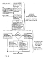
- FIG. 1 there is a block diagram of a conventional data processing system having various complex components which are interconnected by buses.
- a processor bus 10 connects the central control component, the processing unit 1, to a main memory (MM) 4 via a cache/main storage controller (cache CTL/ST-CTL) 3/5 and a main memory bus (MM-bus) 13.
- Processor bus 10 also connects the processor to an optional floating point processor 8 and at least to one I/O bus adapter 7.
- the I/O bus adapter connects processor bus 10 via an Input/Output bus (I/O bus) 9 to various Input/Output devices (I/O DEVs), and to further components such as communication adapters (COMM) etc.
- I/O bus adapter 7 is further designed to connect various control and monitoring components to the system, such as a customer engineering panel CE-P, a battery operated time of day clock TOD a read only memory unit ROM, an operator panel PAN, a power controller PWR-CTL or two supplementary devices SUPPL.
- a control store (CNTL-ST) 2 containing the control program is connected to the PU via a separate control store bus 11.
- the system clock generation and distribution is centralized on a clock chip (CLCK) 6 which has multi-wire connections 14 to almost all of the system components.
- CLCK clock chip
- three initialization/reset areas are defined for processing unit 1.
- any other reasonable number of reset areas can be used.
- the shift register latches are reset by flashing or ripple.
- the level sensitive scan design rules are described in the article "A logic design structure for LSI testability" by E.B. Aichelberger, Proceedings of the Design Automation Conference No. 14, 20-22, June 1977, New La, Louisiana, pp. 462-468.
- the three reset areas are defined below: -
- the S-area power-on reset area
- the I-area system reset area
- SRL shift register latches
- the I-area system reset area
- Latches, however, which are part of maintenance and/or service circuitry are not included.
- a microinstruction address compare register and the respective stop circuits of the PU chip 1 will not be reset. This offers the opportunity of checking and examining the system reset functions under conditions which are set into those registers.
- IML Initial Micro Code Loading
- system Reset with/without clearing the memory
- Loading Off the system program with/without clearing the memory, IPL.
- IML Initial Micro Code Loading
- system Reset with/without clearing the memory
- IPL Loading Off the system program
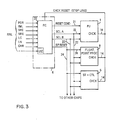
- the reset control (RS) 20 as shown in Fig. 3 is located on clock chip 6. Connected to the reset control 20 are all the reset request lines RRL, on which the signals can cause a total or partial system initialization or reset.
- the signals from top to bottom on the left side of Fig. 3 are the "power on reset” signal POR, the "initial micro program load” signal IML, the "system reset clear” signal SRC, the “system reset normal” signal SRN, the "load clear” signal LC and the "load normal” signal LN. These signals will be explained with more detail later on.
- the reset operations as shown in Fig. 2 are system specific and based on hardware design and architectural requirements.
- reset operations can be arranged in a sequence according to the depth of their clearing effects on the hardware and logic areas within a data processing system.
- the most significant clearing action can be considered as general actions supported by a sequence of single reset actions.
- the other reset actions involve less portions of the logic amount which means that more information is left in its original state.
- the system reset clear signal SRC, the system reset normal signal SRN, the load clear signal LC and the load normal signal LN result in a reset of the latches of the I- and F-area.
- a check reset CHR causes a reset of the latches of the F-area.
- the given reset functions can alternatively be activated via a unit support interface (USI) for remote control purposes.
- USB unit support interface
- the reset control 20 has a set of output lines 21 to 24 for the transfer of various control signals to processor chip 1, floating point processor 8, storage controller 5 and to other chips which might be included in a computer system, an example of which is shown in Fig. 1.
- Output line 21 is used to transfer the reset condition information, three bits in parallel, to the processor chip 1.
- Output lines 22 and 23 distribute the common clock signals, shift clock A (SCL A) and the shift clock B (SCL B), to the various chips. While shift clock A controls the master latches, shift clock B controls the slave latches of the chained shift register latches SRL.
- the reset areas are further controlled by a two-wire line 24 which connects reset control 20 to the various chips with the exception of processor chip 1.
- the four different states of these two lines are sufficient to select the three given reset areas (S-, I-, F-; I - F; and F- only) and to indicate a "no-reset" state.
- Output line 21 consists of three wires thus being able to express 8 different states. These are the 7 different reset causes and one "no-reset" state.
- the 7 reset states are used in a twofold manner: 1) They designate the three reset areas and in addition to the two wire output line 24, they 2) provide the reset causes in detail.
- the reset causes are manifested in the so called reset indicator latches which can only be sensed (read) and reset by microinstructions of the error handling routines.
- the information which is stored in all those reset indicator latches allows a detailed analysis of the reason or cause of a system reset and can be used later on for controlling the microprogram after restarting the computer system.
- Output line 21 extends only to that chip which provides the logic required to access the reset information by microinstruction, which is the PU chip in this specific case.
- Reset control 20 within clock chip 6 is further controlled by check reset signals which are activated by erroneous chips.
- the check reset signals are transmitted via so called stop lines 14 which are explained with more detail in European Patent Application 88 108 138.4.
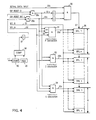
- the direct decoding of the signals on line 24 is used at the receiving side to connect the shift clock A (SCL A) to the master latches of the shift register latches SRL1 ... SRLn, SRL1 ... SRLt, SRL1 ... SRLv of the respective reset area F, I, S.
- Shift clock B (SCL B) is permanently connected to the slave latches of the shift register latches.
- the decoding of the SIF reset bits on line 24 is performed by the AND gates 31 - 34 and OR gate 32. When, for example, only reset area F has to be reset the SIF reset bit combination "01" has to be applied to line 24.
- the inverted bit combination on line 24 is also fed to AND gate 30, together with a serial data input.
- the output signal of AND gate 30 is, in any case a binary zero, with the exception of a code combination "00" which represents, however, a no reset condition, as can be seen in the table.
- AND gate 33 When reset areas F and I are to be reset, e.g. in case of "load normal” (SIF reset code "10"), AND gate 33 will additionally be enabled so that the pulses of shift clock A will be transferred via line 22b to the master latches of the I-area. The binary zero already propagated through the F-area, continues through the I-area latches.
- the pulse diagram and the scheme of resetting the latches of shift register chain 35 which are represented in Fig. 5 show with more detail how the system is operated.
- the first two lines on top of Fig. 5 show the pulses of the shift clock A applied to the master latches, and of shift clock B for the slave latches of the shift register latches in shift register chain 35.
- Line three shows a situation where a reset request, e.g. "system reset clear” (SRC) came in on line RRL.
- SRC system reset clear
- Line 11 shows the pulses of gated shift clock A which is available on lines 22a and 22b.
- Fig. 5 shows the zero propagation through latches LT1 to LT2048 which form the shift register chain in this example.
- the zero is transferred from its master latch M to its slave latch S.
- all latches or stages are reset to zero.
- the maximum length of a reset chain in a given system determines the maximum count of counter 40 which is located in reset control 20.
- the counter is incremented in a close relationship to the shift clock pulses, and its count is transferred to a comparator 38.
- Register 39 is used to store a value which is equal to a preferred or selected number of shift register stages forming a chain, in the present example equal to the number 2048.
- AND gate 30 generates the binary zero for propagation. Whenever the bits of the SIF reset code on line 24 differ from zero a binary zero is forced at the input D1 of chain 35 independent of what level is provided on the Serial Data Input line 22z which, in a non-reset state, provides the serial input data to the chain input D1.
Priority Applications (6)
| Application Number | Priority Date | Filing Date | Title |
|---|---|---|---|
| EP88114023A EP0356538B1 (de) | 1988-08-27 | 1988-08-27 | Einrichtung in einem Datenverarbeitungssystem zur System-Initialisierung und -Rückstellung |
| DE3886529T DE3886529T2 (de) | 1988-08-27 | 1988-08-27 | Einrichtung in einem Datenverarbeitungssystem zur System-Initialisierung und -Rückstellung. |
| JP1192792A JPH0642186B2 (ja) | 1988-08-27 | 1989-07-27 | データ処理システム |
| KR1019890012045A KR920004277B1 (ko) | 1988-08-27 | 1989-08-24 | 시스템 초기화 및 리세트용 데이타 처리 시스템내의 장치 |
| CN89106663A CN1015134B (zh) | 1988-08-27 | 1989-08-26 | 在数据处理系统中使系统初始化和复位的装置 |
| US07/401,332 US5155856A (en) | 1988-08-27 | 1989-08-31 | Arrangement in a self-guarding data processing system for system initialization and reset |
Applications Claiming Priority (1)
| Application Number | Priority Date | Filing Date | Title |
|---|---|---|---|
| EP88114023A EP0356538B1 (de) | 1988-08-27 | 1988-08-27 | Einrichtung in einem Datenverarbeitungssystem zur System-Initialisierung und -Rückstellung |
Publications (2)
| Publication Number | Publication Date |
|---|---|
| EP0356538A1 true EP0356538A1 (de) | 1990-03-07 |
| EP0356538B1 EP0356538B1 (de) | 1993-12-22 |
Family
ID=8199235
Family Applications (1)
| Application Number | Title | Priority Date | Filing Date |
|---|---|---|---|
| EP88114023A Expired - Lifetime EP0356538B1 (de) | 1988-08-27 | 1988-08-27 | Einrichtung in einem Datenverarbeitungssystem zur System-Initialisierung und -Rückstellung |
Country Status (6)
| Country | Link |
|---|---|
| US (1) | US5155856A (de) |
| EP (1) | EP0356538B1 (de) |
| JP (1) | JPH0642186B2 (de) |
| KR (1) | KR920004277B1 (de) |
| CN (1) | CN1015134B (de) |
| DE (1) | DE3886529T2 (de) |
Cited By (7)
| Publication number | Priority date | Publication date | Assignee | Title |
|---|---|---|---|---|
| EP0524642A2 (de) * | 1991-07-24 | 1993-01-27 | Nec Corporation | Register-Steuerungsschaltung zur Initialisierung von Registern |
| AU637227B2 (en) * | 1990-04-13 | 1993-05-20 | Fujitsu Limited | Method of resetting adapter module at failing time and computer system |
| EP0752655A1 (de) * | 1995-06-26 | 1997-01-08 | Motorola, Inc. | Datenverarbeitungssystem und Verfahren dafür |
| WO1997017645A2 (de) * | 1995-11-08 | 1997-05-15 | Siemens Nixdorf | Schnelleinschaltungsverfahren |
| EP0903587A2 (de) * | 1997-09-18 | 1999-03-24 | Siemens Aktiengesellschaft | Verfahren zum Testen einer elektronischen Schaltung |
| EP1253507A2 (de) * | 2001-04-26 | 2002-10-30 | Fujitsu Limited | Prozessor und Verfahren zum Steuern der Rückstellungssequenz des Prozessors |
| KR100763173B1 (ko) * | 1999-11-23 | 2007-10-08 | 프리스케일 세미컨덕터, 인크. | 리셋 후 데이터 처리 시스템을 구성하는 장치 및 방법 |
Families Citing this family (27)
| Publication number | Priority date | Publication date | Assignee | Title |
|---|---|---|---|---|
| EP0548077B1 (de) * | 1990-01-05 | 2002-04-24 | Sun Microsystems, Inc. | Aktiver hochgeschwindigkeitsbus |
| US5271019A (en) * | 1991-03-15 | 1993-12-14 | Amdahl Corporation | Scannable system with addressable scan reset groups |
| US5390324A (en) * | 1992-10-02 | 1995-02-14 | Compaq Computer Corporation | Computer failure recovery and alert system |
| US5568380A (en) * | 1993-08-30 | 1996-10-22 | International Business Machines Corporation | Shadow register file for instruction rollback |
| GB2281986B (en) * | 1993-09-15 | 1997-08-06 | Advanced Risc Mach Ltd | Data processing reset |
| WO1995012848A1 (en) * | 1993-11-03 | 1995-05-11 | Eo, Inc. | Recovery boot process |
| US5898232A (en) * | 1995-11-08 | 1999-04-27 | Advanced Micro Devices, Inc. | Input/output section of an integrated circuit having separate power down capability |
| US5860125A (en) * | 1995-11-08 | 1999-01-12 | Advanced Micro Devices, Inc. | Integrated circuit including a real time clock, configuration RAM, and memory controller in a core section which receives an asynchronous partial reset and an asynchronous master reset |
| CN1077988C (zh) * | 1995-12-15 | 2002-01-16 | 盛群半导体股份有限公司 | 系统重置状态的设定装置 |
| DE19612440C1 (de) * | 1996-03-28 | 1997-05-07 | Siemens Ag | Schaltungsanordnung mit einer Anzahl von elektronischen Schaltungskomponenten |
| KR100209762B1 (ko) * | 1996-10-28 | 1999-07-15 | 구본준 | 리셋 장치 및 그를 이용한 동작 모드 설정 방법 |
| CA2402389A1 (en) | 2000-03-08 | 2002-09-19 | Shuffle Master, Inc. | Computerized gaming system, method and apparatus |
| US7043641B1 (en) | 2000-03-08 | 2006-05-09 | Igt | Encryption in a secure computerized gaming system |
| US7988559B2 (en) | 2001-03-08 | 2011-08-02 | Igt | Computerized gaming system, method and apparatus |
| US6792527B1 (en) * | 2000-12-22 | 2004-09-14 | Xilinx, Inc. | Method to provide hierarchical reset capabilities for a configurable system on a chip |
| US7203841B2 (en) * | 2001-03-08 | 2007-04-10 | Igt | Encryption in a secure computerized gaming system |
| US7618317B2 (en) | 2001-09-10 | 2009-11-17 | Jackson Mark D | Method for developing gaming programs compatible with a computerized gaming operating system and apparatus |
| US6902481B2 (en) | 2001-09-28 | 2005-06-07 | Igt | Decoupling of the graphical presentation of a game from the presentation logic |
| US7931533B2 (en) | 2001-09-28 | 2011-04-26 | Igt | Game development architecture that decouples the game logic from the graphics logics |
| US8708828B2 (en) | 2001-09-28 | 2014-04-29 | Igt | Pluggable modular gaming modifiers and configuration templates for gaming environments |
| EP1463569A4 (de) | 2001-11-26 | 2010-06-02 | Igt Reno Nev | Vorrichtung und verfahren zur unverzögerten durchgangsvalidierung |
| US7194671B2 (en) * | 2001-12-31 | 2007-03-20 | Intel Corporation | Mechanism handling race conditions in FRC-enabled processors |
| US6954886B2 (en) * | 2001-12-31 | 2005-10-11 | Intel Corporation | Deterministic hardware reset for FRC machine |
| US7055060B2 (en) * | 2002-12-19 | 2006-05-30 | Intel Corporation | On-die mechanism for high-reliability processor |
| JP4294503B2 (ja) * | 2003-07-31 | 2009-07-15 | 富士通マイクロエレクトロニクス株式会社 | 動作モード制御回路、動作モード制御回路を含むマイクロコンピュータ及びそのマイクロコンピュータを利用した制御システム |
| CN101840259B (zh) * | 2010-04-30 | 2013-03-13 | 北京星网锐捷网络技术有限公司 | 复位方法及复位控制装置 |
| CN109361368A (zh) * | 2018-12-14 | 2019-02-19 | 无锡思泰迪半导体有限公司 | 一种带复位功能的集成比较器的滤波器及其控制方法 |
Citations (1)
| Publication number | Priority date | Publication date | Assignee | Title |
|---|---|---|---|---|
| US4625312A (en) * | 1983-10-06 | 1986-11-25 | Honeywell Information Systems Inc. | Test and maintenance method and apparatus for investigation of intermittent faults in a data processing system |
Family Cites Families (10)
| Publication number | Priority date | Publication date | Assignee | Title |
|---|---|---|---|---|
| FR2432175A1 (fr) * | 1978-07-27 | 1980-02-22 | Cii Honeywell Bull | Procede pour tester un systeme logique et systeme logique pour la mise en oeuvre de ce procede |
| JPS5935072B2 (ja) * | 1978-09-22 | 1984-08-27 | 松下電器産業株式会社 | バス運行デ−タ収集装置 |
| DE2842750A1 (de) * | 1978-09-30 | 1980-04-10 | Ibm Deutschland | Verfahren und anordnung zur pruefung von durch monolithisch integrierten halbleiterschaltungen dargestellten sequentiellen schaltungen |
| JPS5854418A (ja) * | 1981-09-28 | 1983-03-31 | Hitachi Ltd | 割込み処理方式 |
| US4503386A (en) * | 1982-04-20 | 1985-03-05 | International Business Machines Corporation | Chip partitioning aid (CPA)-A structure for test pattern generation for large logic networks |
| JPS5920025A (ja) * | 1982-07-27 | 1984-02-01 | Toshiba Corp | 半導体集積回路の初期化装置 |
| US4752907A (en) * | 1983-08-31 | 1988-06-21 | Amdahl Corporation | Integrated circuit scanning apparatus having scanning data lines for connecting selected data locations to an I/O terminal |
| JPS61267110A (ja) * | 1985-05-21 | 1986-11-26 | Mitsubishi Electric Corp | 情報処理装置のレジスタ初期化方式 |
| DE3603751A1 (de) * | 1986-02-06 | 1987-08-13 | Siemens Ag | Informationsuebergabesystem zur uebergabe von binaeren informationen |
| US4958274A (en) * | 1988-06-01 | 1990-09-18 | Digital Equipment Corporation | System with a N stages timing silo and P stages information silo for soloing information |
-
1988
- 1988-08-27 DE DE3886529T patent/DE3886529T2/de not_active Expired - Fee Related
- 1988-08-27 EP EP88114023A patent/EP0356538B1/de not_active Expired - Lifetime
-
1989
- 1989-07-27 JP JP1192792A patent/JPH0642186B2/ja not_active Expired - Fee Related
- 1989-08-24 KR KR1019890012045A patent/KR920004277B1/ko not_active IP Right Cessation
- 1989-08-26 CN CN89106663A patent/CN1015134B/zh not_active Expired
- 1989-08-31 US US07/401,332 patent/US5155856A/en not_active Expired - Fee Related
Patent Citations (1)
| Publication number | Priority date | Publication date | Assignee | Title |
|---|---|---|---|---|
| US4625312A (en) * | 1983-10-06 | 1986-11-25 | Honeywell Information Systems Inc. | Test and maintenance method and apparatus for investigation of intermittent faults in a data processing system |
Non-Patent Citations (2)
| Title |
|---|
| IBM TECHNICAL DISCLOSURE BULLETIN * |
| PATENT ABSTRACTS OF JAPAN * |
Cited By (15)
| Publication number | Priority date | Publication date | Assignee | Title |
|---|---|---|---|---|
| AU637227B2 (en) * | 1990-04-13 | 1993-05-20 | Fujitsu Limited | Method of resetting adapter module at failing time and computer system |
| US5321830A (en) * | 1990-04-13 | 1994-06-14 | Fujitsu Limited | Reset method when adaptor module is faulty and computer system executing same |
| EP0524642A2 (de) * | 1991-07-24 | 1993-01-27 | Nec Corporation | Register-Steuerungsschaltung zur Initialisierung von Registern |
| EP0524642A3 (de) * | 1991-07-24 | 1994-02-09 | Nec Corp | |
| EP0752655A1 (de) * | 1995-06-26 | 1997-01-08 | Motorola, Inc. | Datenverarbeitungssystem und Verfahren dafür |
| WO1997017645A3 (de) * | 1995-11-08 | 1997-07-03 | Siemens Nixdorf Inf Syst | Schnelleinschaltungsverfahren |
| WO1997017645A2 (de) * | 1995-11-08 | 1997-05-15 | Siemens Nixdorf | Schnelleinschaltungsverfahren |
| US6212643B1 (en) | 1995-11-08 | 2001-04-03 | Siemens Nixdorf Informationssysteme Aktiengesellschaft | High-speed connection method |
| EP0903587A2 (de) * | 1997-09-18 | 1999-03-24 | Siemens Aktiengesellschaft | Verfahren zum Testen einer elektronischen Schaltung |
| EP0903587A3 (de) * | 1997-09-18 | 1999-10-20 | Siemens Aktiengesellschaft | Verfahren zum Testen einer elektronischen Schaltung |
| US6308291B1 (en) | 1997-09-18 | 2001-10-23 | Siemens Aktiengesellschaft Ag | Method for testing an electronic circuit |
| KR100763173B1 (ko) * | 1999-11-23 | 2007-10-08 | 프리스케일 세미컨덕터, 인크. | 리셋 후 데이터 처리 시스템을 구성하는 장치 및 방법 |
| EP1253507A2 (de) * | 2001-04-26 | 2002-10-30 | Fujitsu Limited | Prozessor und Verfahren zum Steuern der Rückstellungssequenz des Prozessors |
| EP1253507A3 (de) * | 2001-04-26 | 2004-06-16 | Fujitsu Limited | Prozessor und Verfahren zum Steuern der Rückstellungssequenz des Prozessors |
| US6963969B2 (en) | 2001-04-26 | 2005-11-08 | Fujitsu Limited | Method and processor for initializing a plurality of non-overlapping areas with associated flags and signals |
Also Published As
| Publication number | Publication date |
|---|---|
| DE3886529T2 (de) | 1994-06-30 |
| EP0356538B1 (de) | 1993-12-22 |
| KR920004277B1 (ko) | 1992-06-01 |
| US5155856A (en) | 1992-10-13 |
| JPH0642186B2 (ja) | 1994-06-01 |
| DE3886529D1 (de) | 1994-02-03 |
| CN1040691A (zh) | 1990-03-21 |
| JPH0281216A (ja) | 1990-03-22 |
| CN1015134B (zh) | 1991-12-18 |
| KR900003740A (ko) | 1990-03-27 |
Similar Documents
| Publication | Publication Date | Title |
|---|---|---|
| EP0356538B1 (de) | Einrichtung in einem Datenverarbeitungssystem zur System-Initialisierung und -Rückstellung | |
| US7962816B2 (en) | I/O switches and serializer for each parallel scan register | |
| US4621363A (en) | Testing and diagnostic device for digital computers | |
| US4710927A (en) | Diagnostic circuit | |
| US4630041A (en) | Enhanced reliability interrupt control apparatus | |
| US4488259A (en) | On chip monitor | |
| US4688222A (en) | Built-in parallel testing circuit for use in a processor | |
| US4019033A (en) | Control store checking system and method | |
| US5677915A (en) | Customized method and apparatus for streamlined testing a particular electrical circuit | |
| US7013415B1 (en) | IC with internal interface switch for testability | |
| GB1581864A (en) | Logic systems | |
| US3980839A (en) | Maintenance monitor for telephone switching systems | |
| US4225921A (en) | Transfer control technique between two units included in a data processing system | |
| US5515530A (en) | Method and apparatus for asynchronous, bi-directional communication between first and second logic elements having a fixed priority arbitrator | |
| US4432050A (en) | Data processing system write protection mechanism | |
| US4217639A (en) | Logic for generating multiple clock pulses within a single clock cycle | |
| US4236210A (en) | Architecture for a control store included in a data processing system | |
| KR900008804B1 (ko) | 선견 터미날 카운터 및 터미날 카운트 신호 발생 방법 | |
| US4396981A (en) | Control store apparatus having dual mode operation handling mechanism | |
| CN115344105A (zh) | 接口复用的芯片和芯片的调试系统 | |
| EP0523438A2 (de) | Mikrorechner mit "Boundary-Scan"-Gerät | |
| JPH0219931A (ja) | マイクロプロセッサのテストモード制御方式 | |
| SU959086A1 (ru) | Устройство дл диагностики двухмашинного вычислительного комплекса | |
| SU1275458A1 (ru) | Однородна вычислительна система | |
| CN114528034A (zh) | 加载电路、方法和系统 |
Legal Events
| Date | Code | Title | Description |
|---|---|---|---|
| PUAI | Public reference made under article 153(3) epc to a published international application that has entered the european phase |
Free format text: ORIGINAL CODE: 0009012 |
|
| AK | Designated contracting states |
Kind code of ref document: A1 Designated state(s): DE FR GB IT |
|
| 17P | Request for examination filed |
Effective date: 19900621 |
|
| 17Q | First examination report despatched |
Effective date: 19921012 |
|
| GRAA | (expected) grant |
Free format text: ORIGINAL CODE: 0009210 |
|
| AK | Designated contracting states |
Kind code of ref document: B1 Designated state(s): DE FR GB IT |
|
| PG25 | Lapsed in a contracting state [announced via postgrant information from national office to epo] |
Ref country code: IT Free format text: LAPSE BECAUSE OF FAILURE TO SUBMIT A TRANSLATION OF THE DESCRIPTION OR TO PAY THE FEE WITHIN THE PRE;WARNING: LAPSES OF ITALIAN PATENTS WITH EFFECTIVE DATE BEFORE 2007 MAY HAVE OCCURRED AT ANY TIME BEFORE 2007. THE CORRECT EFFECTIVE DATE MAY BE DIFFERENT FROM THE ONE RECORDED.SCRIBED TIME-LIMIT Effective date: 19931222 |
|
| REF | Corresponds to: |
Ref document number: 3886529 Country of ref document: DE Date of ref document: 19940203 |
|
| ET | Fr: translation filed | ||
| PLBE | No opposition filed within time limit |
Free format text: ORIGINAL CODE: 0009261 |
|
| STAA | Information on the status of an ep patent application or granted ep patent |
Free format text: STATUS: NO OPPOSITION FILED WITHIN TIME LIMIT |
|
| 26N | No opposition filed | ||
| PGFP | Annual fee paid to national office [announced via postgrant information from national office to epo] |
Ref country code: DE Payment date: 19950821 Year of fee payment: 8 |
|
| PGFP | Annual fee paid to national office [announced via postgrant information from national office to epo] |
Ref country code: GB Payment date: 19960724 Year of fee payment: 9 |
|
| PGFP | Annual fee paid to national office [announced via postgrant information from national office to epo] |
Ref country code: FR Payment date: 19960806 Year of fee payment: 9 |
|
| PG25 | Lapsed in a contracting state [announced via postgrant information from national office to epo] |
Ref country code: DE Effective date: 19970501 |
|
| PG25 | Lapsed in a contracting state [announced via postgrant information from national office to epo] |
Ref country code: GB Free format text: LAPSE BECAUSE OF NON-PAYMENT OF DUE FEES Effective date: 19970827 |
|
| GBPC | Gb: european patent ceased through non-payment of renewal fee |
Effective date: 19970827 |
|
| PG25 | Lapsed in a contracting state [announced via postgrant information from national office to epo] |
Ref country code: FR Free format text: LAPSE BECAUSE OF NON-PAYMENT OF DUE FEES Effective date: 19980430 |
|
| REG | Reference to a national code |
Ref country code: FR Ref legal event code: ST |