EP0350929A2 - Verarbeitungssysteme für variable Datenlänge - Google Patents
Verarbeitungssysteme für variable Datenlänge Download PDFInfo
- Publication number
- EP0350929A2 EP0350929A2 EP89112869A EP89112869A EP0350929A2 EP 0350929 A2 EP0350929 A2 EP 0350929A2 EP 89112869 A EP89112869 A EP 89112869A EP 89112869 A EP89112869 A EP 89112869A EP 0350929 A2 EP0350929 A2 EP 0350929A2
- Authority
- EP
- European Patent Office
- Prior art keywords
- address
- data
- bus
- delimiter
- register
- Prior art date
- Legal status (The legal status is an assumption and is not a legal conclusion. Google has not performed a legal analysis and makes no representation as to the accuracy of the status listed.)
- Granted
Links
- 238000012545 processing Methods 0.000 title claims description 46
- 238000001514 detection method Methods 0.000 claims description 27
- 230000004044 response Effects 0.000 claims description 6
- 230000015572 biosynthetic process Effects 0.000 description 10
- 230000000875 corresponding effect Effects 0.000 description 6
- 101150089655 Ins2 gene Proteins 0.000 description 5
- 101100072652 Xenopus laevis ins-b gene Proteins 0.000 description 5
- 101100179596 Caenorhabditis elegans ins-3 gene Proteins 0.000 description 4
- 238000013500 data storage Methods 0.000 description 4
- 238000010586 diagram Methods 0.000 description 2
- 238000000034 method Methods 0.000 description 2
- 230000008569 process Effects 0.000 description 2
- 230000001276 controlling effect Effects 0.000 description 1
- 125000004122 cyclic group Chemical group 0.000 description 1
- 238000012986 modification Methods 0.000 description 1
- 230000004048 modification Effects 0.000 description 1
Images


Classifications
-
- G—PHYSICS
- G06—COMPUTING; CALCULATING OR COUNTING
- G06F—ELECTRIC DIGITAL DATA PROCESSING
- G06F12/00—Accessing, addressing or allocating within memory systems or architectures
- G06F12/02—Addressing or allocation; Relocation
- G06F12/04—Addressing variable-length words or parts of words
Definitions
- the present invention relates to an apparatus for processing variable length data in which words, records, files, and the like are delimited by delimiter codes.
- variable length data When data processing is performed in a variable length data format, processed variable length data are delimited by word and record delimiter codes in units of words and records, and are sequentially arrayed and stored on a memory.
- the variable length data string When processing is performed for the variable length data string arrayed and stored on the memory, the variable length data string is sequentially read out from the memory and the word and record delimiter codes are retrieved. For example, when a second word in each record in the memory is extracted to perform updating processing, a record delimiter code in the memory is retrieved, and a first word delimiter code from the retrieved record delimiter code is retrieved to extract the second word (because the second word is arrayed to follow the first word). In order to extract the second word in each record, the above retrieval processing must be repetitively executed.
- a word to be processed in each record is predetermined, e.g., a variable word is a second word and other words are fixed words.
- the retrieval processing must be executed every time processing for the word to be processed is performed.
- a data processing apparatus which accesses storage means storing variable length data delimited by delimiter codes to perform data processing, comprising: controlling means, connected to said storage means through an address bus, for designating an address through said address bus every time one clock is generated, reading out data stored at the designated address onto a data bus, and incrementing the address every time the data is read out; detecting means, connected to said data bus, for detecting in response to every clock whether or not the data on said data bus coincides with the delimiter code indicating a delimitation of a data block; latching means, connected to said address bus, for, when said detecting means detects a coincidence, latching the address on said address bus; table means for storing address data based on the address latched in said latching means; and processing means for designating a start address of each data block stored in said storage means with reference to the address data stored in said table means and performing processing for each data block.
- a table based on addresses indicating delimiter positions of variable length data stored in a memory can be easily formed.
- desired data in the memory is read out and processing, e.g., updating of the readout data is to be performed, high-speed access can be performed by utilizing the table.
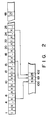
- Fig. 1 is a block diagram of a variable length data processing apparatus according to an embodiment of the present invention.
- the variable length data processing apparatus processes variable length data in which words and records are delimited by delimiter codes.
- the apparatus processes variable length data stored in a RAM 3 in accordance with a program prestored in a ROM 2 under the control of a CPU 1.
- the RAM 3 is connected to the CPU 1 and the ROM 2 through an address bus AB and a data bus DB.
- the address bus AB and the data bus DB are connected to a magnetic disk 4 for storing a large volume of variable length data and a DMA controller 5 for directly transferring a portion of the variable length data stored in the magnetic disk 4.
- the address bus AB and the data bus DB are also connected to a delimiter detection unit 6.
- the delimiter detection unit 6 detects various delimiter codes, i.e., a delimiter code "," indicating a delimitation of a word, a delimiter code "(" indicating a delimitation of a record, a delimiter code " " a delimitation of a file, and the like, on the data bus DB, reads out an address in the RAM 3 in which the detected delimiter code is stored, and performs various processing operations such as creation of an address table based on the readout address under the control of a controller 61.
- the delimiter detection unit 6 includes an address generator 62 and an address latch circuit 63 which are connected to both the data bus DB and the address bus AB, and a designated field register 64, an instruction code register 65, a delimiter type register 66, a read buffer 67, and a detector 68 which are connected to the data bus DB.
- the designated field register 64 is connected to a comparator 69.
- the comparator 69 is connected to a counter 70.
- the instruction code register 65 is connected to an instruction decoder 71. A decoded output from the instruction decoder is supplied to the controller 61.
- the address generator 62 has a read address register RA and a write address register WA.
- the generator 62 Upon reception of a start signal S2 from the controller 61, the generator 62 starts a cyclic operation consisting of a read cycle and a write cycle on the basis of a clock signal generated by a clock generator (not shown).
- the generator 62 outputs the content of the read address register RA onto the address bus AB.
- the generator 62 increments the content of the read address register by "1".
- the generator 62 When the generator 62 receives a latch completion signal S8 from the controller 61, it outputs the content of the write address register WA onto the address bus AB, and increments the content of the write address register WA by "1" after the lapse of a predetermined period of time from the outputting.
- the address latch circuit 63 Upon reception of an address latch signal S6 from the controller 61, the address latch circuit 63 fetches the address data present on the address bus AB at that time, increments the data by "1", and outputs it onto the data bus DB.
- the designated field register 64 stores data indicating the order of words to be designated on one record. When this data is supplied to the comparator 69, it is decremented by "1" and is compared with the content of the counter 70.
- the instruction code register 65 stores an instruction code determining the operation of the delimiter detection unit 6.
- the register 65 causes the instruction decoder 71 to decode a table formation instruction code INS1, a specific field table formation instruction Code INS2, a data transfer instruction code INS3, or the like in accordance with the instruction code, thus determining the control operation of the controller 61.
- the delimiter codes ",”, “(", “ “, and the like are preset in the delimiter type register 66, and are supplied to the detector 68.
- the detector 68 is a circuit for detecting whether or not the content of the read buffer 67 for temporarily storing data read out from the RAM 3 onto the data bus DB coincides with any one of the delimiter codes preset in the delimiter type register 66.
- the detector outputs a detection signal of the corresponding delimiter code to the controller 61.
- the detector outputs no detection signal.
- the controller 61 performs a control operation in accordance with the instruction code set in the instruction code register 65. For example, when the specific field table formation instruction code INS2 is set in the instruction code register 65, the controller 61 performs signal I/O control as follows.
- the controller 61 When the data transfer instruction code INS3 is set in the instruction code register 65, the controller 61 performs signal I/O control as follows.
- the DMA controller 5 will now be described.
- the DMA controller 5 has an address counter AC.
- the controller 5 receives the start signal S10 from the controller 61, it starts a data transfer operation on the basis of a clock signal from a clock generator (not shown).
- the controller 5 reads out unit data from the magnetic disk 4 onto the data bus DB, and outputs the content of the address counter AC onto the address bus AB to designate an address of the RAM 3.
- the controller 5 transfers the unit data on the data bus DB to the designated address position in the RAM 3.
- the controller 5 repeats this operation in response to every clock signal, so that each unit data in the magnetic disk 4 is transferred to the RAM 3 at high speed.
- the address counter AC is incremented by "1" every time the unit data is transferred.
- the DMA controller 5 When the DMA controller 5 receives the interruption signal S11 from the controller 61, it interrupts the data transfer operation (stops a clock operation), and then sends the interrupted signal S12 to the controller 61. Upon reception of the interruption completion signal S13 from the controller 61, the DMA controller 5 restarts the interrupted data transfer operation. Upon reception of an end signal S14, the controller 5 ends a series of data transfer operations.
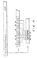
- Fig. 2 shows a case wherein the start address of a second word of each record stored in an area starting from address "1" in the RAM 3 is written in a table area of the RAM 3, i.e., a table area starting from address "100", thereby forming an address table. Since the start address of the second word of the first record is "5", the address "5" data is written at address "100". Since the start address of the second word of the second record is "16”, the address "16" data is written at address "101”. Since the start address of the second word of the third record is "25”, the address "25” data is written at address "102". Similarly, the start addresses of the second words of the following records are written in an area after address "103", thus forming the address table.
- Various registers are initialized prior to address table formation processing. More specifically, the CPU 1 sets data "1" and “100” as initial values in the read address register RA and the write address register WA, and sets data "2" in the designated field register 64. The CPU 1 then sets the delimiter codes ",”, "(", and " " in the delimiter type register 66, and sets the specific field table formation instruction code INS2 in the instruction code register 65.
- the CPU 1 After these setting operations, the CPU 1 outputs the processing start signal S1 to the controller 61, and transfers all the control to the controller 61.
- the controller 61 Upon reception of the processing start signal S1 from the CPU 1, the controller 61 outputs the start signal S2 to the address generator 62. More specifically, the address generator 62 outputs address data stored in the read address register RA onto the address bus AB in a first read cycle, and reads out data stored in the corresponding address area in the RAM 3 onto the data bus DB. The data read out onto the data bus DB is fetched in the read buffer 67, and the detector 68 judges whether or not the fetched data coincides with any one of the delimiter codes set in the delimiter type register 66. Since data stored in the address area "1" in the RAM 3 is the delimiter code "(", its detection signal is output to the controller 61.
- the controller 61 When the controller 61 receives the detection signal of the delimiter code "(", it outputs the reset signal S3 to the counter 70 to reset the content of the counter 70 to "1". Since no address latch operation is performed in this read cycle, the address generator 62 does not output address data stored in the write address register WA onto the address bus AB in the following write cycle, and no write access to the RAM 3 is performed. Upon completion of the read cycle, the value of the read address register RA is incremented by "1", i.e., to "2".
- the content of the read address register RA is output onto the address bus AB, and data, i.e., "x" stored in the corresponding address area in the RAM 3 is read out onto the data bus DB.
- This data is fetched in the read buffer 67. Since this data is not a delimiter code, the detector 68 does not output a detection signal, and hence, no write access to the RAM 3 is performed in the following write cycle.
- the controller 61 When the controller 61 receives the coincidence signal S5, it outputs the latch signal S6 to the address latch circuit 63. Thus, the address latch circuit 63 latches address data at that time, i.e., "4". Thereafter, the controller 61 outputs the count-up signal S7 to the counter 70 to update the value of the counter 70 to "2". The controller 61 outputs the latch completion signal S8 to the address generator 62. The address generator 62 outputs address data, i.e., "100", stored in the write address register WA onto the address bus AB to designate the corresponding address area in the RAM 3.
- the controller 61 In the sixth read cycle, since the delimiter code ",” is detected on the data bus DB, this code is detected by the detector 68, and its detection result is supplied to the controller 61. Upon reception of this detection signal, the controller 61 outputs the comparison signal S4 to the comparator 69, so that a value "1” obtained by decrementing data stored in the designated field register 64 by "1" is compared with a count value stored in the counter 70. In this case, since the counter 70 stores data "2", the comparator 69 does not output the coincidence signal S5. As a result, the controller 61 does not output the latch signal S6 to the address latch circuit 63, and hence, no data storage processing is performed in the following write cycle. In this read cycle, the controller 61 outputs the count-up signal S7 to the counter 70 to update the value of the counter 70 to "3".
- the data readout processing is sequentially performed.
- this code is detected by the detector 68, and its detection result is supplied to the controller 61.
- the controller 61 Upon reception of this detection signal, the controller 61 outputs the reset signal S3 to the counter 70 to reset the content of the counter 70 to "1".
- the delimiter code "” is output onto the data bus DB, and this code is detected by the detector 68.
- the controller 61 then supplies the comparison signal S4 to the comparator 69, so that a value "1” obtained by decrementing data stored in the designated field register 64 by "1” is compared with a count value stored in the counter 70.
- the comparator 69 outputs the coincidence signal S5, and the controller 61 outputs the latch signal S6 to the address latch circuit 63 to cause it to latch address data at that time, i.e., "15".
- the controller 61 outputs the count-up signal S7 to the counter 70, and outputs the latch completion signal S8 to the address generator 62.
- the address generator 62 outputs address data, i.e., "101" stored in the write address register WA onto the address bus AB in the following write cycle. In this case, data obtained by incrementing the address data latched in the address latch circuit 63 by "1", i.e., data "16” is supplied onto the data bus DB. This data "16” is stored at address "101" in the RAM 3.
- the data stored in the RAM 3 are sequentially read out, and are subjected to delimiter detection in the detector 68. If the delimiter code "(" indicating the record delimitation is detected, the counter 70 is detected. If the delimiter code "," indicating a word delimitation is detected, the comparator 69 checks if this code is a code stored immediately before the designated word in one record, i.e., a delimiter code stored immediately before the second word. If it is determined that the detected code is the delimiter code stored immediately before the second word, the address in the RAM 3 at which this delimiter code is stored is latched in the address latch circuit 63. Data obtained by incrementing this address value by "1" is sequentially stored in the table area in the RAM 3.
- the controller 61 ends the address table formation processing, and outputs the end signal S9 to the CPU 1, thus transferring all the control to the CPU 1.
- the start addresses of the second words of the records in a predetermined file in the RAM 3 are stored in the designated address table area in the RAM 3.
- the CPU 1 refers to the address table to directly detect the start addresses of the second words of the records in the file, and updating processing or the like for one file can be performed at high speed.
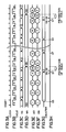
- Fig. 4 shows a case wherein variable-length word data stored in the magnetic disk 4 are sequentially transferred to and stored in an area starting from address "11" in the RAM 3, and at the same time, the start address of the words stored in the RAM 3 in this manner are stored in the table area in the RAM 3, i.e., in an area starting from address "100", thus forming an address table. Since the start addresses of the words are "12", “15”, “17”, “21”, “24”, "26",..., they are stored at addresses "100”, "101", "102",... to form the address table.
- the data are transferred from the magnetic disk 4 to the RAM 3, and at the same time, the address table storing the start addresses of the words stored in the RAM 3 is formed. Therefore, after the above-mentioned data transfer, a desired word can be directly accessed based on the address table, and updating processing of words, or the like can be performed at high speed.
- the CPU 1 sets data "100” as an initial value in the write address register WA, and sets data "11” as an initial value in the address counter AC of the DMA controller 5.
- the CPU 1 sets the delimiter codes ",”, "(", and " " in the delimiter type register 66, and sets the data transfer instruction code INS3 in the instruction code register 65.
- the CPU 1 After these setting operations, the CPU 1 outputs the processing start signal S1 to the controller 61, thus transferring all the control to the controller 61.
- the controller 61 Upon reception of the processing start signal S1 from the CPU 1, the controller 61 outputs the start signal S10 to the DMA controller 5. More specifically, the DMA controller 5 outputs the address data stored in the address counter AC onto the address bus AB, and at the same time, reads out unit data from the magnetic disk 4. Since the address counter AC stores the data "11" as the initial value, address "11" of the RAM 3 is designated, and data stored at the start address of the magnetic disk 4, i.e., the delimiter code "(" is read out onto the data bus DB. The readout code is stored at address "11" of the RAM 3.
- the data read out onto the data bus DB is fetched in the read buffer 67 at the same time, and it is checked if the fetched code coincides with the delimiter code set in the delimiter type register 66.
- the readout data is the delimiter code "("
- its detection signal is output to the controller 61.
- the controller 61 Upon reception of the detection signal, the controller 61 outputs the latch signal S6 to the address latch circuit 63 to cause it to latch address data at that time, i.e., "11".
- the DMA controller 5 increments the value of the address counter AC by "1" to "12". Thereafter, the controller 61 outputs the interruption signal S11 to the DMA controller 5.
- the DMA controller 5 Upon reception of the interruption signal S11, the DMA controller 5 temporarily interrupts the readout operation of the data from the magnetic disk 4, and outputs the interrupted signal S12 to the controller 61.
- the controller 61 receives the interrupted signal S12, it outputs the latch completion signal S8 to the address generator 62.
- the address generator 62 outputs address data stored in the write address register WA, i.e., "100" onto the address bus AB, and designates the corresponding address in the RAM 3.
- data obtained by incrementing address data latched in the address latch circuit 63 by "1", i.e., data "12” is supplied onto the data bus DB.
- the data "12" on the data bus DB is stored at address "100" in the RAM 3.
- the address generator 62 increments the value of the write address register WA by "1". Thereafter, the controller 61 outputs the interruption completion signal S13 to the DMA controller 5. Upon reception of the interruption completion signal S13, the DMA controller 5 restarts the data readout operation.
- the DMA controller 5 When the DMA controller 5 restarts the data readout operation, it outputs address data stored in the address counter AC onto the address bus AB in synchronism with the clock, and at the same time, reads out unit data from the magnetic disk 4. Since the address counter AC stores data "12", address "12" of the RAM 3 is designated, and the second data stored in the magnetic disk 4, i.e., data "x” is read out onto the data bus DB, and is stored at address "12" of the RAM 3. The data read out onto the data bus DB is fetched in the read buffer 67 at the same time, and the detector 68 judges whether or not the fetched data is the delimiter code set in the delimiter type register 66.
- the detector 68 since the readout data is not a delimiter code, the detector 68 outputs no detection signal, and only the data transfer operation is performed. After the data storage operation in the RAM 3, the value of the address counter AC is incremented by "1" to "13".
- the third unit data stored in the magnetic disk 4 is transferred to address "13" of the RAM 3. Since this data is not a delimiter code, either, only the data transfer operation is performed.
- the fourth unit data stored in the magnetic disk 4 is transferred to address "14" of the RAM 3. Since this data is the delimiter code ",”, the detector 68 outputs a detection signal. Upon reception of the detection signal, the controller 61 outputs the latch signal S6 to the address latch circuit 63 to cause it to latch address data at that time, i.e., "14". The latched address data is incremented by "1", and the incremented data "15" is stored at an address designated by the address generator 62, i.e., address "101" in the RAM 3.
- the controller 61 When the detector 68 detects the delimiter code " " indicating a file delimitation, the controller 61 outputs an operation end signal S14 to the DMA controller 5, thus stopping the data transfer operation of the DMA controller 5. The controller 61 outputs the end signal S9 to the CPU 1 to transfer all the control to the CPU 1.
- variable length data for one file stored in the magnetic disk 4 are transferred to the RAM 3, and the storage position of each transferred word in the RAM 3, i.e., the start address of each word is stored in the predetermined address table area in the RAM 3.
- the CPU 1 can refer to the address table to directly detect the storage position of a word, and perform high-speed word access.
- the operations based on the specific field table formation instruction code INS2 and the data transfer instruction code INS3 have been described.
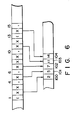
- An operation based on the table formation instruction code INS1 is performed in the same manner as described above. More specifically, the operation based on the table formation instruction code INS1 corresponds to a partial modification of the operation based on the instruction code INS2. That is, when the detector 68 detects the delimiter code "," or "(", the latch signal S6 is output based on this detection. Therefore, in this case, the start addresses of all the words are stored in the address stored. Fig. 6 shows this state.
- an address table indicating only a delimitation position of each word an address table indicating only a delimitation position of each record, and an address table indicating only a delimitation position of each file, can be arbitrarily formed.
Landscapes
- Engineering & Computer Science (AREA)
- Theoretical Computer Science (AREA)
- Physics & Mathematics (AREA)
- General Engineering & Computer Science (AREA)
- General Physics & Mathematics (AREA)
- Information Retrieval, Db Structures And Fs Structures Therefor (AREA)
- Signal Processing For Digital Recording And Reproducing (AREA)
- Bus Control (AREA)
- Compression, Expansion, Code Conversion, And Decoders (AREA)
Applications Claiming Priority (6)
| Application Number | Priority Date | Filing Date | Title |
|---|---|---|---|
| JP175111/88 | 1988-07-15 | ||
| JP17511188A JPH0225922A (ja) | 1988-07-15 | 1988-07-15 | データ検出装置 |
| JP311346/88 | 1988-12-09 | ||
| JP31134688A JPH02157933A (ja) | 1988-12-09 | 1988-12-09 | 可変長データ処理装置 |
| JP311347/88 | 1988-12-09 | ||
| JP31134788A JPH02157934A (ja) | 1988-12-09 | 1988-12-09 | 可変長データ処理装置 |
Publications (3)
| Publication Number | Publication Date |
|---|---|
| EP0350929A2 true EP0350929A2 (de) | 1990-01-17 |
| EP0350929A3 EP0350929A3 (de) | 1991-01-30 |
| EP0350929B1 EP0350929B1 (de) | 1995-09-27 |
Family
ID=27324044
Family Applications (1)
| Application Number | Title | Priority Date | Filing Date |
|---|---|---|---|
| EP89112869A Expired - Lifetime EP0350929B1 (de) | 1988-07-15 | 1989-07-13 | Verarbeitungssysteme für variable Datenlänge |
Country Status (5)
| Country | Link |
|---|---|
| US (1) | US5115490A (de) |
| EP (1) | EP0350929B1 (de) |
| KR (1) | KR0152979B1 (de) |
| CA (1) | CA1324684C (de) |
| DE (1) | DE68924377T2 (de) |
Families Citing this family (19)
| Publication number | Priority date | Publication date | Assignee | Title |
|---|---|---|---|---|
| CA1328027C (en) * | 1988-07-14 | 1994-03-22 | Toshio Kashio | Data processing apparatus |
| JPH0795269B2 (ja) * | 1988-11-04 | 1995-10-11 | 富士通株式会社 | 命令コードのデコード装置 |
| JP2746734B2 (ja) * | 1990-06-08 | 1998-05-06 | 富士通株式会社 | ストリームファイルに対してのアクセス処理方式 |
| US5510785A (en) * | 1993-03-19 | 1996-04-23 | Sony Corporation | Method of coding a digital signal, method of generating a coding table, coding apparatus and coding method |
| JP3433978B2 (ja) * | 1993-07-30 | 2003-08-04 | 富士通株式会社 | 入出力制御装置 |
| US5586253A (en) * | 1994-12-15 | 1996-12-17 | Stratus Computer | Method and apparatus for validating I/O addresses in a fault-tolerant computer system |
| JPH1021012A (ja) * | 1996-06-28 | 1998-01-23 | Toshiba Corp | 磁気ディスク装置及び同装置のコマンド処理方法 |
| WO2001065479A2 (en) * | 2000-03-03 | 2001-09-07 | Koninklijke Philips Electronics N.V. | Data carrier having means for synchronization with a received data stream |
| US6901481B2 (en) | 2000-04-14 | 2005-05-31 | Stratus Technologies Bermuda Ltd. | Method and apparatus for storing transactional information in persistent memory |
| US6802022B1 (en) | 2000-04-14 | 2004-10-05 | Stratus Technologies Bermuda Ltd. | Maintenance of consistent, redundant mass storage images |
| US6862689B2 (en) | 2001-04-12 | 2005-03-01 | Stratus Technologies Bermuda Ltd. | Method and apparatus for managing session information |
| US7137108B1 (en) * | 2000-10-26 | 2006-11-14 | International Business Machines Corporation | Identifying non-externalized text strings that are not hard-coded |
| US6948010B2 (en) * | 2000-12-20 | 2005-09-20 | Stratus Technologies Bermuda Ltd. | Method and apparatus for efficiently moving portions of a memory block |
| US6886171B2 (en) * | 2001-02-20 | 2005-04-26 | Stratus Technologies Bermuda Ltd. | Caching for I/O virtual address translation and validation using device drivers |
| US6766413B2 (en) | 2001-03-01 | 2004-07-20 | Stratus Technologies Bermuda Ltd. | Systems and methods for caching with file-level granularity |
| US6874102B2 (en) * | 2001-03-05 | 2005-03-29 | Stratus Technologies Bermuda Ltd. | Coordinated recalibration of high bandwidth memories in a multiprocessor computer |
| US6996750B2 (en) * | 2001-05-31 | 2006-02-07 | Stratus Technologies Bermuda Ltd. | Methods and apparatus for computer bus error termination |
| DE10324014A1 (de) * | 2003-05-27 | 2005-01-13 | Micronas Gmbh | Adressgenerator, Betriebsverfahren dafür und diesen verwendendes Daten verarbeitendes System |
| KR100963140B1 (ko) * | 2008-11-27 | 2010-06-16 | 한국과학기술원 | 직접 메모리 접근 장치 및 직접 메모리 접근 방법 |
Citations (4)
| Publication number | Priority date | Publication date | Assignee | Title |
|---|---|---|---|---|
| US4133041A (en) * | 1975-12-25 | 1979-01-02 | Casio Computer Co., Ltd. | Data processing control apparatus with selective data readout |
| WO1981000633A1 (en) * | 1979-08-31 | 1981-03-05 | Western Electric Co | Special address generation arrangement |
| EP0032075A1 (de) * | 1979-12-20 | 1981-07-15 | COMPAGNIE INTERNATIONALE POUR L'INFORMATIQUE CII - HONEYWELL BULL (dite CII-HB) | Adressierungsvorrichtung für Informationselemente in einer Mehreingangstabelle, welche in einem Speicher geschrieben steht |
| JPS59116870A (ja) * | 1982-12-23 | 1984-07-05 | Casio Comput Co Ltd | デ−タ記憶装置 |
Family Cites Families (15)
| Publication number | Priority date | Publication date | Assignee | Title |
|---|---|---|---|---|
| JPS5235264B2 (de) * | 1971-09-29 | 1977-09-08 | ||
| JPS5413306B2 (de) * | 1974-01-24 | 1979-05-30 | ||
| CA1071332A (en) * | 1974-05-01 | 1980-02-05 | Toshio Kashio | Data processing system |
| JPS586979B2 (ja) * | 1974-11-15 | 1983-02-07 | カシオケイサンキ カブシキガイシヤ | ジヨウホウヨミダシソウチ |
| JPS5522821B2 (de) * | 1974-11-15 | 1980-06-19 | ||
| JPS5524134B2 (de) * | 1974-11-15 | 1980-06-27 | ||
| JPS5250132A (en) * | 1975-10-21 | 1977-04-21 | Casio Comput Co Ltd | Information processing control unit |
| JPS5272125A (en) * | 1975-12-12 | 1977-06-16 | Casio Comput Co Ltd | Manual input device for information |
| JPS5346689A (en) * | 1976-10-12 | 1978-04-26 | Sumitomo Electric Ind Ltd | Oil removing method and device empolyed when welding of cable |
| JPS5350953A (en) * | 1976-10-20 | 1978-05-09 | Casio Comput Co Ltd | Comparison/array system for variable length information |
| US4376933A (en) * | 1979-02-22 | 1983-03-15 | Xerox Corporation | Circuit for compacting data |
| FR2486926A1 (fr) * | 1980-07-21 | 1982-01-22 | Saint Gobain Vitrage | Four pour le chauffage de feuilles de verre suspendues en position verticale |
| JPS5845920B2 (ja) * | 1980-09-19 | 1983-10-13 | 荏原インフイルコ株式会社 | 有機性廃液の生物化学的処理方法 |
| JPS5846735A (ja) * | 1981-09-15 | 1983-03-18 | Anritsu Corp | 2チヤネル波形記憶装置 |
| JPS5853384A (ja) * | 1981-09-25 | 1983-03-29 | Toshiba Corp | レ−ザシ−ム溶接機 |
-
1989
- 1989-06-24 KR KR1019890008774A patent/KR0152979B1/ko not_active IP Right Cessation
- 1989-07-03 US US07/375,386 patent/US5115490A/en not_active Expired - Fee Related
- 1989-07-05 CA CA000604840A patent/CA1324684C/en not_active Expired - Fee Related
- 1989-07-13 DE DE68924377T patent/DE68924377T2/de not_active Expired - Fee Related
- 1989-07-13 EP EP89112869A patent/EP0350929B1/de not_active Expired - Lifetime
Patent Citations (4)
| Publication number | Priority date | Publication date | Assignee | Title |
|---|---|---|---|---|
| US4133041A (en) * | 1975-12-25 | 1979-01-02 | Casio Computer Co., Ltd. | Data processing control apparatus with selective data readout |
| WO1981000633A1 (en) * | 1979-08-31 | 1981-03-05 | Western Electric Co | Special address generation arrangement |
| EP0032075A1 (de) * | 1979-12-20 | 1981-07-15 | COMPAGNIE INTERNATIONALE POUR L'INFORMATIQUE CII - HONEYWELL BULL (dite CII-HB) | Adressierungsvorrichtung für Informationselemente in einer Mehreingangstabelle, welche in einem Speicher geschrieben steht |
| JPS59116870A (ja) * | 1982-12-23 | 1984-07-05 | Casio Comput Co Ltd | デ−タ記憶装置 |
Non-Patent Citations (1)
| Title |
|---|
| PATENT ABSTRACTS OF JAPAN vol. 8, no. 242 (P-311)(1679) 07 November 1984, & JP-A-59 116870 (CASIO KEISANKI K.K.) 05 July 1984, * |
Also Published As
| Publication number | Publication date |
|---|---|
| KR0152979B1 (ko) | 1998-11-16 |
| EP0350929A3 (de) | 1991-01-30 |
| US5115490A (en) | 1992-05-19 |
| EP0350929B1 (de) | 1995-09-27 |
| DE68924377D1 (de) | 1995-11-02 |
| CA1324684C (en) | 1993-11-23 |
| KR900002170A (ko) | 1990-02-28 |
| DE68924377T2 (de) | 1996-03-07 |
Similar Documents
| Publication | Publication Date | Title |
|---|---|---|
| EP0350929A2 (de) | Verarbeitungssysteme für variable Datenlänge | |
| US3848235A (en) | Scan and read control apparatus for a disk storage drive in a computer system | |
| US3510847A (en) | Address manipulation circuitry for a digital computer | |
| US4747045A (en) | Information processing apparatus having an instruction prefetch circuit | |
| EP0404126A3 (de) | Cache-Speicher mit der Möglichkeit im Fehlgriffsfall gleichzeitig zu aktualisieren und eine Entscheidung über die nächste Adresse zu treffen | |
| US4885682A (en) | Microprogram controller for detecting the occurrence of an interrupt request or a termination of a string instruction | |
| US3480917A (en) | Arrangement for transferring between program sequences in a data processor | |
| JPH0449142B2 (de) | ||
| KR100249536B1 (ko) | 다수의 버스를 서로 독립적으로 제어하기 위한 버스콘트롤러를 가진 데이터 처리기 | |
| JPH0743647B2 (ja) | データ処理装置における命令ループ捕捉機構 | |
| JPH0748647B2 (ja) | デューティ比判別回路 | |
| KR0153537B1 (ko) | 메모리 번지 데이타를 선행 선택하는 신호처리 구조 | |
| JP3045731B2 (ja) | シーケンス制御方式 | |
| JPS59123055A (ja) | 命令処理方式 | |
| SU1439605A1 (ru) | Устройство дл сопр жени процессора с пам тью | |
| JP2586172B2 (ja) | 学習機能付テーブル検索装置 | |
| JPH05181906A (ja) | 記憶装置 | |
| EP0381225A2 (de) | Mikroprogrammsteuereinrichtung zur schnelleren Durchführung von Befehlen zum Transfer von Datenfolgen | |
| JPS61264465A (ja) | デ−タ転送制御方式 | |
| JPH0642248B2 (ja) | 情報検索装置 | |
| JPS6167106A (ja) | シ−ケンス回路の高速検索方式 | |
| JPH056273A (ja) | 演算処理装置 | |
| JPS6091461A (ja) | マイクロプロセツサのデ−タアドレス空間拡張装置 | |
| JPH04363723A (ja) | 演算処理装置 | |
| JPS5917470B2 (ja) | 記憶装置のプログラムエリアとデ−タエリアの可変方式 |
Legal Events
| Date | Code | Title | Description |
|---|---|---|---|
| PUAI | Public reference made under article 153(3) epc to a published international application that has entered the european phase |
Free format text: ORIGINAL CODE: 0009012 |
|
| AK | Designated contracting states |
Kind code of ref document: A2 Designated state(s): DE FR GB IT NL |
|
| PUAL | Search report despatched |
Free format text: ORIGINAL CODE: 0009013 |
|
| RHK1 | Main classification (correction) |
Ipc: G06F 12/04 |
|
| AK | Designated contracting states |
Kind code of ref document: A3 Designated state(s): DE FR GB IT NL |
|
| 17P | Request for examination filed |
Effective date: 19910322 |
|
| 17Q | First examination report despatched |
Effective date: 19940919 |
|
| GRAA | (expected) grant |
Free format text: ORIGINAL CODE: 0009210 |
|
| AK | Designated contracting states |
Kind code of ref document: B1 Designated state(s): DE FR GB IT NL |
|
| ITF | It: translation for a ep patent filed | ||
| REF | Corresponds to: |
Ref document number: 68924377 Country of ref document: DE Date of ref document: 19951102 |
|
| ET | Fr: translation filed | ||
| PLBE | No opposition filed within time limit |
Free format text: ORIGINAL CODE: 0009261 |
|
| STAA | Information on the status of an ep patent application or granted ep patent |
Free format text: STATUS: NO OPPOSITION FILED WITHIN TIME LIMIT |
|
| 26N | No opposition filed | ||
| PGFP | Annual fee paid to national office [announced via postgrant information from national office to epo] |
Ref country code: GB Payment date: 19980706 Year of fee payment: 10 |
|
| PGFP | Annual fee paid to national office [announced via postgrant information from national office to epo] |
Ref country code: FR Payment date: 19980709 Year of fee payment: 10 |
|
| PGFP | Annual fee paid to national office [announced via postgrant information from national office to epo] |
Ref country code: DE Payment date: 19980720 Year of fee payment: 10 |
|
| PGFP | Annual fee paid to national office [announced via postgrant information from national office to epo] |
Ref country code: NL Payment date: 19980728 Year of fee payment: 10 |
|
| PG25 | Lapsed in a contracting state [announced via postgrant information from national office to epo] |
Ref country code: GB Free format text: LAPSE BECAUSE OF NON-PAYMENT OF DUE FEES Effective date: 19990713 |
|
| PG25 | Lapsed in a contracting state [announced via postgrant information from national office to epo] |
Ref country code: FR Free format text: THE PATENT HAS BEEN ANNULLED BY A DECISION OF A NATIONAL AUTHORITY Effective date: 19990731 |
|
| PG25 | Lapsed in a contracting state [announced via postgrant information from national office to epo] |
Ref country code: NL Free format text: LAPSE BECAUSE OF NON-PAYMENT OF DUE FEES Effective date: 20000201 |
|
| GBPC | Gb: european patent ceased through non-payment of renewal fee |
Effective date: 19990713 |
|
| NLV4 | Nl: lapsed or anulled due to non-payment of the annual fee |
Effective date: 20000201 |
|
| PG25 | Lapsed in a contracting state [announced via postgrant information from national office to epo] |
Ref country code: DE Free format text: LAPSE BECAUSE OF NON-PAYMENT OF DUE FEES Effective date: 20000503 |
|
| REG | Reference to a national code |
Ref country code: FR Ref legal event code: ST |
|
| PG25 | Lapsed in a contracting state [announced via postgrant information from national office to epo] |
Ref country code: IT Free format text: LAPSE BECAUSE OF NON-PAYMENT OF DUE FEES;WARNING: LAPSES OF ITALIAN PATENTS WITH EFFECTIVE DATE BEFORE 2007 MAY HAVE OCCURRED AT ANY TIME BEFORE 2007. THE CORRECT EFFECTIVE DATE MAY BE DIFFERENT FROM THE ONE RECORDED. Effective date: 20050713 |