EP0343879A2 - Transistor bipolaire et sa méthode de fabrication - Google Patents
Transistor bipolaire et sa méthode de fabrication Download PDFInfo
- Publication number
- EP0343879A2 EP0343879A2 EP89305113A EP89305113A EP0343879A2 EP 0343879 A2 EP0343879 A2 EP 0343879A2 EP 89305113 A EP89305113 A EP 89305113A EP 89305113 A EP89305113 A EP 89305113A EP 0343879 A2 EP0343879 A2 EP 0343879A2
- Authority
- EP
- European Patent Office
- Prior art keywords
- region
- layer
- bipolar transistor
- major surface
- base
- Prior art date
- Legal status (The legal status is an assumption and is not a legal conclusion. Google has not performed a legal analysis and makes no representation as to the accuracy of the status listed.)
- Granted
Links
Images

Classifications
-
- H—ELECTRICITY
- H10—SEMICONDUCTOR DEVICES; ELECTRIC SOLID-STATE DEVICES NOT OTHERWISE PROVIDED FOR
- H10D—INORGANIC ELECTRIC SEMICONDUCTOR DEVICES
- H10D64/00—Electrodes of devices having potential barriers
- H10D64/111—Field plates
-
- H—ELECTRICITY
- H10—SEMICONDUCTOR DEVICES; ELECTRIC SOLID-STATE DEVICES NOT OTHERWISE PROVIDED FOR
- H10D—INORGANIC ELECTRIC SEMICONDUCTOR DEVICES
- H10D62/00—Semiconductor bodies, or regions thereof, of devices having potential barriers
- H10D62/10—Shapes, relative sizes or dispositions of the regions of the semiconductor bodies; Shapes of the semiconductor bodies
- H10D62/13—Semiconductor regions connected to electrodes carrying current to be rectified, amplified or switched, e.g. source or drain regions
- H10D62/133—Emitter regions of BJTs
- H10D62/135—Non-interconnected multi-emitter structures
-
- H—ELECTRICITY
- H10—SEMICONDUCTOR DEVICES; ELECTRIC SOLID-STATE DEVICES NOT OTHERWISE PROVIDED FOR
- H10D—INORGANIC ELECTRIC SEMICONDUCTOR DEVICES
- H10D84/00—Integrated devices formed in or on semiconductor substrates that comprise only semiconducting layers, e.g. on Si wafers or on GaAs-on-Si wafers
- H10D84/101—Integrated devices comprising main components and built-in components, e.g. IGBT having built-in freewheel diode
- H10D84/121—BJTs having built-in components
- H10D84/125—BJTs having built-in components the built-in components being resistive elements, e.g. BJT having a built-in ballasting resistor
-
- H—ELECTRICITY
- H10—SEMICONDUCTOR DEVICES; ELECTRIC SOLID-STATE DEVICES NOT OTHERWISE PROVIDED FOR
- H10D—INORGANIC ELECTRIC SEMICONDUCTOR DEVICES
- H10D84/00—Integrated devices formed in or on semiconductor substrates that comprise only semiconducting layers, e.g. on Si wafers or on GaAs-on-Si wafers
- H10D84/40—Integrated devices formed in or on semiconductor substrates that comprise only semiconducting layers, e.g. on Si wafers or on GaAs-on-Si wafers characterised by the integration of at least one component covered by groups H10D12/00 or H10D30/00 with at least one component covered by groups H10D10/00 or H10D18/00, e.g. integration of IGFETs with BJTs
- H10D84/401—Combinations of FETs or IGBTs with BJTs
Definitions
- the present invention relates to a bipolar transistor.
- MOS transistor integrated circuits In the field of MOS transistor integrated circuits, its has become the practice to form the gates of the transistors of polysilicon which is doped to make it conductive. Also, the polysilicon gates are generally used to mask the channel region of the transistors while forming the source and drain regions on opposite sides of the gates so that the source and drain regions are aligned with their respective gate. Recently there has been developed integrated circuits which include both MOS transistors and bipolar devices so that the circuits can perform both analog and digital functions. In such circuit, a layer of doped polysilicon is provided for making the MOS transistors.
- a bipolar transistor including a body of a semiconductor material having a major surface.
- a first region of one conductivity type is in the body and at the major surface.
- a second region of the opposite conductivity type is in the first region and at the major surface.
- a third region of the one conductivity type is in the second region with the junction between the second and third regions at the body surface being spaced from the junction between the first and second regions at the body surface.
- a layer of conductive polycrystalline silicon is over and insulated from the major surface of the body and extends over the area of the surface between the junctions.
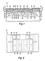
- a bipolar transistor is formed on a substrate 12 of a semiconductor material, such as single crystalline silicon, of one conductivity type, such as P-type.
- the substrate 12 may have formed therein or thereon other components, such as MOS transistors and other bipolar devices, which form a desired electrical circuit.
- a body 16 of the semiconductor material of the opposite conductivity type, such as N-type having a major surface 18.
- the body 16 may be a layer of the semiconductor material which was epitaxially deposited on the substrate surface 14.
- the body 16 includes a thin region 20 along the substrate surface 14 which is highly conductive, i.e. an N+ type region, and highly conductive, N+ type, contact regions 22 extending through the body 16 to the highly conductive region 20. This forms a well region 24 of N-type conductivity in the body 16 which is the collector of the bipolar transistor 10.
- the emitter regions 30 are arranged in rows and columns. Each of the emitter regions 30 forms a junction 32 with the base region 26 which extends to the surface 18.
- the emitter/base junctions 32 of the emitter regions 30 which are adjacent the base/collector junction 28 are spaced from the base/collector junction 28.
- highly conductive regions 34 of the one conductivity type i.e. P+ type, which serve as contacts to the base region 26.
- a highly conductive collector contact region 36 of the opposite conductivity type ie. N+ type.
- the polysilicon layer 40 includes a pair of narrow strips 42 which extend over and along the area of the surface 18 between the collector/base junction 28 and the emitter/base junctions 32 of the emitter regions 26 which are adjacent the collector/base junction 28.
- the polysilicon strips 42 are used as masks to define the space between the collector/base junction 28 and the adjacent emitter/base junctions 32 and thereby define an electrical characteristic of the transistor 10.
- the polysilicon strips 40 serve as an emitter/base field shield.
- Each of the polysilicon strips 40 extends to one end of a substantially rectangular area 44 of the polysilicon which is at one end of the emitter regions 30.
- the polysilicon areas 44 serve as emitter ballast resistors and have openings 46 therethrough which define the resistance of the resistors.
- a first level metalization is on the silicon oxide layer 48.
- the first level metalization will usually be a layer of a conductive metal, such as aluminum, but may be a layer of doped polysilicon.
- the conductive layer is defined to form conductors extending between the various portions of the transistor 10. As shown in FIGURE 3, the first level metalization includes emitter conductors 50 which extend between the emitter regions 30 and through openings in the silicon oxide layers 48 and 38 to make ohmic contact to the emitter regions 30.
- the emitter conductors 50 also extend over one end of the resistors 44 and extend through openings in the silicon oxide layer 48 to make ohmic contact to the resistors 44. Thus, the emitter regions 30 are electrically connected to the resistors 44.
- Base conductors 52 extend between the base contact regions 34 and through openings in the silicon oxide layers 48 and 38 to make ohmic contact to the base contact regions 34.
- the conductors 50 and 52 extend to separate terminal pads, not shown, at the edges of the transistor 10 where conductors from other components in the circuit can be connected to the emitter and base of the transistor 10.
- a second level metalization is on the silicon oxide layer 54.
- the second level metalization is also usually a layer of a conductive metal, such as aluminum, but may be a layer of doped polysilicon which is defined to form conductors.
- the second level metalization is formed into collector conductors 56 which extend through openings in the silicon oxide layers 54, 48 and 38 to make ohmic contact to the collector contact regions 36.
- the second level metalization also includes conductors, not shown, which extend through openings in the silicon oxide layers 54 and 48 to make ohmic contact to the other ends of the resistors 44.
- the silicon oxide insulating layer 38 is formed on the body surface 18.
- a layer of doped polysilicon is then deposited on the silicon oxide layer 38 and defined to form the strips 42 and resistors 44. If the bipolar transistor 10 is being made as part of an integrated circuit which also includes MOS transistors, the polysilicon layer is also defined to form the gates of the MOS transistors.
- the emitter regions 30 are then formed in the base region 26 such as by diffusion or ion implantation using the strips 42 as a mask to define the spacing between the collector/base junction 28 and the emitter/base junctions 32 which are adjacent the collector base junction 28 at the surface 18. Since this spacing determines certain electrical characteristics of the bipolar transistor 10, by using the strips 42 to define this spacing, the spacing can be easily and accurately controlled to provide the desired characteristics for the bipolar transistor 10.
- a bipolar transistor 10 having a layer of conductive polysilicon, a portion of which serves as a mask to define the spacing between the collector/base junction and the emitter/base junction so as to define certain electrical characteristics of the bipolar transistor 10.
- the same conductive polysilicon layer can be used to form the gates of the MOS transistors.
- the same portions of the doped polysilicon layer which serve as the masking shield also serve as an emitter/base field shield which is connected to the emitters 30 through the emitter conductors 50 which contact the polysilicon layer at the resistors 44 so as to be at the emitter potential.
- the doped polysilicon layer includes resistor regions 44 which are connected to the emitters 30 to serve as ballast resistors for the bipolar transistor 10.
- the doped polysilicon layer 40 serves a number of different functions in the bipolar transistor 10 both in the making of the transistor and its operation.
- the bipolar transistor 10 has been described as having N-type conductivity collector and emitter regions and a P-type conductivity base region to form a NPN transistor, the conductivity type of the regions can be reversed to form a PNP transistor.
- the bipolar transistor may be formed in an integrated circuit also including MOS transistors, the polysilicon layer being used for both types of transistor.
- the polysilicon layer may form the gates of the MOS transistors.
- the polysilicon layer ballasts and shields the bipolar transistor in the foregoing example.
Landscapes
- Bipolar Transistors (AREA)
- Metal-Oxide And Bipolar Metal-Oxide Semiconductor Integrated Circuits (AREA)
- Bipolar Integrated Circuits (AREA)
Applications Claiming Priority (2)
| Application Number | Priority Date | Filing Date | Title |
|---|---|---|---|
| US07/197,098 US4864379A (en) | 1988-05-20 | 1988-05-20 | Bipolar transistor with field shields |
| US197098 | 1988-05-20 |
Publications (3)
| Publication Number | Publication Date |
|---|---|
| EP0343879A2 true EP0343879A2 (fr) | 1989-11-29 |
| EP0343879A3 EP0343879A3 (en) | 1990-08-16 |
| EP0343879B1 EP0343879B1 (fr) | 1995-12-20 |
Family
ID=22728047
Family Applications (1)
| Application Number | Title | Priority Date | Filing Date |
|---|---|---|---|
| EP89305113A Expired - Lifetime EP0343879B1 (fr) | 1988-05-20 | 1989-05-19 | Transistor bipolaire et sa méthode de fabrication |
Country Status (4)
| Country | Link |
|---|---|
| US (1) | US4864379A (fr) |
| EP (1) | EP0343879B1 (fr) |
| JP (1) | JPH0231426A (fr) |
| DE (1) | DE68925150T2 (fr) |
Cited By (2)
| Publication number | Priority date | Publication date | Assignee | Title |
|---|---|---|---|---|
| EP0691034A4 (fr) * | 1993-03-25 | 1996-03-13 | Micrel Inc | Structure de transistor bipolaire a resistance de charge |
| WO1996026548A1 (fr) * | 1995-02-24 | 1996-08-29 | Telefonaktiebolaget Lm Ericsson | Contournement des resistances de protection d'emetteur pour transistors de puissance haute frequence |
Families Citing this family (5)
| Publication number | Priority date | Publication date | Assignee | Title |
|---|---|---|---|---|
| JPH02168666A (ja) * | 1988-09-29 | 1990-06-28 | Mitsubishi Electric Corp | 相補型半導体装置とその製造方法 |
| US5223735A (en) * | 1988-09-30 | 1993-06-29 | Mitsubishi Denki Kabushiki Kaisha | Semiconductor integrated circuit device in which circuit functions can be remedied or changed and the method for producing the same |
| IT1236797B (it) * | 1989-11-17 | 1993-04-02 | St Microelectronics Srl | Dispositivo monolitico di potenza a semiconduttore di tipo verticale con una protezione contro le correnti parassite. |
| SE509780C2 (sv) * | 1997-07-04 | 1999-03-08 | Ericsson Telefon Ab L M | Bipolär effekttransistor och framställningsförfarande |
| US7029981B2 (en) * | 2004-06-25 | 2006-04-18 | Intersil Americas, Inc. | Radiation hardened bipolar junction transistor |
Family Cites Families (10)
| Publication number | Priority date | Publication date | Assignee | Title |
|---|---|---|---|---|
| US3911473A (en) * | 1968-10-12 | 1975-10-07 | Philips Corp | Improved surface breakdown protection for semiconductor devices |
| JPS5811750B2 (ja) * | 1979-06-04 | 1983-03-04 | 株式会社日立製作所 | 高耐圧抵抗素子 |
| JPS5633876A (en) * | 1979-08-29 | 1981-04-04 | Fujitsu Ltd | Transistor |
| US4298402A (en) * | 1980-02-04 | 1981-11-03 | Fairchild Camera & Instrument Corp. | Method of fabricating self-aligned lateral bipolar transistor utilizing special masking techniques |
| SE423946B (sv) * | 1980-10-08 | 1982-06-14 | Asea Ab | Tyristor anordnad for sjelvtendning |
| US4430663A (en) * | 1981-03-25 | 1984-02-07 | Bell Telephone Laboratories, Incorporated | Prevention of surface channels in silicon semiconductor devices |
| JPS5818964A (ja) * | 1981-07-28 | 1983-02-03 | Fujitsu Ltd | 半導体装置 |
| KR890004495B1 (ko) * | 1984-11-29 | 1989-11-06 | 가부시끼가이샤 도오시바 | 반도체 장치 |
| US4656496A (en) * | 1985-02-04 | 1987-04-07 | National Semiconductor Corporation | Power transistor emitter ballasting |
| JPS62229975A (ja) * | 1986-03-31 | 1987-10-08 | Toshiba Corp | 電力用トランジスタ |
-
1988
- 1988-05-20 US US07/197,098 patent/US4864379A/en not_active Expired - Lifetime
-
1989
- 1989-05-19 DE DE68925150T patent/DE68925150T2/de not_active Expired - Fee Related
- 1989-05-19 EP EP89305113A patent/EP0343879B1/fr not_active Expired - Lifetime
- 1989-05-19 JP JP1124619A patent/JPH0231426A/ja active Pending
Cited By (3)
| Publication number | Priority date | Publication date | Assignee | Title |
|---|---|---|---|---|
| EP0691034A4 (fr) * | 1993-03-25 | 1996-03-13 | Micrel Inc | Structure de transistor bipolaire a resistance de charge |
| WO1996026548A1 (fr) * | 1995-02-24 | 1996-08-29 | Telefonaktiebolaget Lm Ericsson | Contournement des resistances de protection d'emetteur pour transistors de puissance haute frequence |
| US5684326A (en) * | 1995-02-24 | 1997-11-04 | Telefonaktiebolaget L.M. Ericsson | Emitter ballast bypass for radio frequency power transistors |
Also Published As
| Publication number | Publication date |
|---|---|
| EP0343879B1 (fr) | 1995-12-20 |
| DE68925150T2 (de) | 1996-08-01 |
| US4864379A (en) | 1989-09-05 |
| DE68925150D1 (de) | 1996-02-01 |
| EP0343879A3 (en) | 1990-08-16 |
| JPH0231426A (ja) | 1990-02-01 |
Similar Documents
| Publication | Publication Date | Title |
|---|---|---|
| US5017503A (en) | Process for making a bipolar transistor including selective oxidation | |
| JP3214818B2 (ja) | レベルシフト操作を有し、金属クロスオーバを有しない高電圧電力用集積回路 | |
| EP0691034B1 (fr) | Structure de transistor bipolaire a resistance de charge | |
| US4115797A (en) | Integrated injection logic with heavily doped injector base self-aligned with injector emitter and collector | |
| US4057894A (en) | Controllably valued resistor | |
| US4639757A (en) | Power transistor structure having an emitter ballast resistance | |
| EP0036319B1 (fr) | Dispositif semiconducteur | |
| EP0685891A1 (fr) | Diode semi-conductrice intégrée | |
| EP0082331B1 (fr) | Diode Zener à claquage par avalanche localisée sous la surface | |
| KR101232662B1 (ko) | 반도체 디바이스를 형성하는 방법 및 그의 구조 | |
| GB2054263A (en) | Integrated circuit device | |
| EP0343879B1 (fr) | Transistor bipolaire et sa méthode de fabrication | |
| JPH0654795B2 (ja) | 半導体集積回路装置及びその製造方法 | |
| KR0182030B1 (ko) | 바이시모스 트랜지스터 및 그 제조 방법 | |
| US3755722A (en) | Resistor isolation for double mesa transistors | |
| JP2926962B2 (ja) | Mis型電界効果トランジスタを有する半導体装置 | |
| US4786961A (en) | Bipolar transistor with transient suppressor | |
| EP0673072B1 (fr) | Dispositif semi-conducteur comprenant un transistor bipolaire latéral | |
| JPH11501462A (ja) | 表面電界減少型(resurf型)高電圧半導体装置の製造方法及びその製造方法によって製造される半導体装置 | |
| US5444292A (en) | Integrated thin film approach to achieve high ballast levels for overlay structures | |
| JPS6195565A (ja) | エミツタ直列抵抗を有するバイポーラトランジスタの製造方法 | |
| US3777230A (en) | Semiconductor device with isolated circuit elements | |
| JPH03190139A (ja) | 半導体集積回路装置 | |
| JP2692292B2 (ja) | 集積回路装置用縦形バイポーラトランジスタ | |
| JPS6060753A (ja) | 半導体装置 |
Legal Events
| Date | Code | Title | Description |
|---|---|---|---|
| PUAI | Public reference made under article 153(3) epc to a published international application that has entered the european phase |
Free format text: ORIGINAL CODE: 0009012 |
|
| AK | Designated contracting states |
Kind code of ref document: A2 Designated state(s): DE FR GB IT NL |
|
| PUAL | Search report despatched |
Free format text: ORIGINAL CODE: 0009013 |
|
| AK | Designated contracting states |
Kind code of ref document: A3 Designated state(s): DE FR GB IT NL |
|
| 17P | Request for examination filed |
Effective date: 19901210 |
|
| 17Q | First examination report despatched |
Effective date: 19921209 |
|
| RAP1 | Party data changed (applicant data changed or rights of an application transferred) |
Owner name: HARRIS CORPORATION |
|
| GRAA | (expected) grant |
Free format text: ORIGINAL CODE: 0009210 |
|
| AK | Designated contracting states |
Kind code of ref document: B1 Designated state(s): DE FR GB IT NL |
|
| PG25 | Lapsed in a contracting state [announced via postgrant information from national office to epo] |
Ref country code: NL Free format text: LAPSE BECAUSE OF FAILURE TO SUBMIT A TRANSLATION OF THE DESCRIPTION OR TO PAY THE FEE WITHIN THE PRESCRIBED TIME-LIMIT Effective date: 19951220 Ref country code: IT Free format text: LAPSE BECAUSE OF FAILURE TO SUBMIT A TRANSLATION OF THE DESCRIPTION OR TO PAY THE FEE WITHIN THE PRE;WARNING: LAPSES OF ITALIAN PATENTS WITH EFFECTIVE DATE BEFORE 2007 MAY HAVE OCCURRED AT ANY TIME BEFORE 2007. THE CORRECT EFFECTIVE DATE MAY BE DIFFERENT FROM THE ONE RECORDED.SCRIBED TIME-LIMIT Effective date: 19951220 |
|
| ET | Fr: translation filed | ||
| REF | Corresponds to: |
Ref document number: 68925150 Country of ref document: DE Date of ref document: 19960201 |
|
| NLT2 | Nl: modifications (of names), taken from the european patent patent bulletin |
Owner name: HARRIS CORPORATION |
|
| NLV1 | Nl: lapsed or annulled due to failure to fulfill the requirements of art. 29p and 29m of the patents act | ||
| PLBE | No opposition filed within time limit |
Free format text: ORIGINAL CODE: 0009261 |
|
| STAA | Information on the status of an ep patent application or granted ep patent |
Free format text: STATUS: NO OPPOSITION FILED WITHIN TIME LIMIT |
|
| 26N | No opposition filed | ||
| REG | Reference to a national code |
Ref country code: GB Ref legal event code: IF02 |
|
| PGFP | Annual fee paid to national office [announced via postgrant information from national office to epo] |
Ref country code: GB Payment date: 20040512 Year of fee payment: 16 |
|
| PGFP | Annual fee paid to national office [announced via postgrant information from national office to epo] |
Ref country code: FR Payment date: 20040519 Year of fee payment: 16 |
|
| PGFP | Annual fee paid to national office [announced via postgrant information from national office to epo] |
Ref country code: DE Payment date: 20040630 Year of fee payment: 16 |
|
| PG25 | Lapsed in a contracting state [announced via postgrant information from national office to epo] |
Ref country code: GB Free format text: LAPSE BECAUSE OF NON-PAYMENT OF DUE FEES Effective date: 20050519 |
|
| PG25 | Lapsed in a contracting state [announced via postgrant information from national office to epo] |
Ref country code: DE Free format text: LAPSE BECAUSE OF NON-PAYMENT OF DUE FEES Effective date: 20051201 |
|
| GBPC | Gb: european patent ceased through non-payment of renewal fee |
Effective date: 20050519 |
|
| PG25 | Lapsed in a contracting state [announced via postgrant information from national office to epo] |
Ref country code: FR Free format text: LAPSE BECAUSE OF NON-PAYMENT OF DUE FEES Effective date: 20060131 |
|
| REG | Reference to a national code |
Ref country code: FR Ref legal event code: ST Effective date: 20060131 |