EP0342846B1 - Système de protection des données dans un système de traitement de données - Google Patents
Système de protection des données dans un système de traitement de données Download PDFInfo
- Publication number
- EP0342846B1 EP0342846B1 EP89304682A EP89304682A EP0342846B1 EP 0342846 B1 EP0342846 B1 EP 0342846B1 EP 89304682 A EP89304682 A EP 89304682A EP 89304682 A EP89304682 A EP 89304682A EP 0342846 B1 EP0342846 B1 EP 0342846B1
- Authority
- EP
- European Patent Office
- Prior art keywords
- battery
- voltage
- data
- signal
- write
- Prior art date
- Legal status (The legal status is an assumption and is not a legal conclusion. Google has not performed a legal analysis and makes no representation as to the accuracy of the status listed.)
- Expired - Lifetime
Links
- 230000015654 memory Effects 0.000 claims description 85
- 238000010586 diagram Methods 0.000 description 9
- 238000001514 detection method Methods 0.000 description 5
- 238000012423 maintenance Methods 0.000 description 5
- 230000006866 deterioration Effects 0.000 description 3
- 230000002159 abnormal effect Effects 0.000 description 2
- 238000003491 array Methods 0.000 description 1
- 230000007547 defect Effects 0.000 description 1
- 230000006870 function Effects 0.000 description 1
- 238000000034 method Methods 0.000 description 1
- 230000007935 neutral effect Effects 0.000 description 1
- 238000011084 recovery Methods 0.000 description 1
- 230000004044 response Effects 0.000 description 1
- 230000003068 static effect Effects 0.000 description 1
Images


Classifications
-
- H—ELECTRICITY
- H02—GENERATION; CONVERSION OR DISTRIBUTION OF ELECTRIC POWER
- H02J—CIRCUIT ARRANGEMENTS OR SYSTEMS FOR SUPPLYING OR DISTRIBUTING ELECTRIC POWER; SYSTEMS FOR STORING ELECTRIC ENERGY
- H02J9/00—Circuit arrangements for emergency or stand-by power supply, e.g. for emergency lighting
-
- G—PHYSICS
- G06—COMPUTING; CALCULATING OR COUNTING
- G06F—ELECTRIC DIGITAL DATA PROCESSING
- G06F11/00—Error detection; Error correction; Monitoring
- G06F11/07—Responding to the occurrence of a fault, e.g. fault tolerance
- G06F11/0703—Error or fault processing not based on redundancy, i.e. by taking additional measures to deal with the error or fault not making use of redundancy in operation, in hardware, or in data representation
- G06F11/0751—Error or fault detection not based on redundancy
- G06F11/0754—Error or fault detection not based on redundancy by exceeding limits
-
- G—PHYSICS
- G06—COMPUTING; CALCULATING OR COUNTING
- G06F—ELECTRIC DIGITAL DATA PROCESSING
- G06F1/00—Details not covered by groups G06F3/00 - G06F13/00 and G06F21/00
- G06F1/26—Power supply means, e.g. regulation thereof
- G06F1/30—Means for acting in the event of power-supply failure or interruption, e.g. power-supply fluctuations
-
- G—PHYSICS
- G06—COMPUTING; CALCULATING OR COUNTING
- G06F—ELECTRIC DIGITAL DATA PROCESSING
- G06F12/00—Accessing, addressing or allocating within memory systems or architectures
- G06F12/02—Addressing or allocation; Relocation
- G06F12/08—Addressing or allocation; Relocation in hierarchically structured memory systems, e.g. virtual memory systems
- G06F12/0802—Addressing of a memory level in which the access to the desired data or data block requires associative addressing means, e.g. caches
- G06F12/0866—Addressing of a memory level in which the access to the desired data or data block requires associative addressing means, e.g. caches for peripheral storage systems, e.g. disk cache
- G06F12/0868—Data transfer between cache memory and other subsystems, e.g. storage devices or host systems
-
- G—PHYSICS
- G06—COMPUTING; CALCULATING OR COUNTING
- G06F—ELECTRIC DIGITAL DATA PROCESSING
- G06F12/00—Accessing, addressing or allocating within memory systems or architectures
- G06F12/02—Addressing or allocation; Relocation
- G06F12/08—Addressing or allocation; Relocation in hierarchically structured memory systems, e.g. virtual memory systems
- G06F12/0802—Addressing of a memory level in which the access to the desired data or data block requires associative addressing means, e.g. caches
- G06F12/0866—Addressing of a memory level in which the access to the desired data or data block requires associative addressing means, e.g. caches for peripheral storage systems, e.g. disk cache
- G06F12/0871—Allocation or management of cache space
-
- G—PHYSICS
- G11—INFORMATION STORAGE
- G11C—STATIC STORES
- G11C5/00—Details of stores covered by group G11C11/00
- G11C5/14—Power supply arrangements, e.g. power down, chip selection or deselection, layout of wirings or power grids, or multiple supply levels
-
- G—PHYSICS
- G11—INFORMATION STORAGE
- G11C—STATIC STORES
- G11C5/00—Details of stores covered by group G11C11/00
- G11C5/14—Power supply arrangements, e.g. power down, chip selection or deselection, layout of wirings or power grids, or multiple supply levels
- G11C5/141—Battery and back-up supplies
-
- G—PHYSICS
- G11—INFORMATION STORAGE
- G11C—STATIC STORES
- G11C7/00—Arrangements for writing information into, or reading information out from, a digital store
- G11C7/22—Read-write [R-W] timing or clocking circuits; Read-write [R-W] control signal generators or management
-
- G—PHYSICS
- G06—COMPUTING; CALCULATING OR COUNTING
- G06F—ELECTRIC DIGITAL DATA PROCESSING
- G06F2212/00—Indexing scheme relating to accessing, addressing or allocation within memory systems or architectures
- G06F2212/10—Providing a specific technical effect
- G06F2212/1032—Reliability improvement, data loss prevention, degraded operation etc
-
- G—PHYSICS
- G06—COMPUTING; CALCULATING OR COUNTING
- G06F—ELECTRIC DIGITAL DATA PROCESSING
- G06F2212/00—Indexing scheme relating to accessing, addressing or allocation within memory systems or architectures
- G06F2212/31—Providing disk cache in a specific location of a storage system
- G06F2212/312—In storage controller
Definitions
- the present invention relates to a data protection system for a memory having a battery to protect the data stored in the memory from accidental power OFF, more particularly, it relates to a battery voltage protection system for protecting a non-volatile type memory provided in a device controller, for example, a disk controller between a channel system and an external storage device in a data processing system.
- a non-volatile type memory having a battery back-up system which can protect the data from accidental power OFF, is widely utilized in data processing systems.
- the battery must be always sufficiently charged to deal with an accidental power OFF. That is, if the battery is always sufficiently charged when the power supply is normal, it is possible to perform the back-up operation when the power source is accidentally interrupted.
- this memory is utilized for storing not only relatively unimportant data, for example, log data for recovering the system, but also relatively important data, for example, a user's data. Accordingly, the battery back-up system must operate precisely to protect the important data from an accidental power OFF so that it is necessary to always check the battery back-up function.
- Japanese Unexamined Patent Publication (Kokai) No. 58-146099 discloses a memory protection system utilizing this patrol check.
- the battery voltage is checked in such a way that it is compared with a reference voltage after the power source is disconnected. That is, Fig. 4 of the reference, the switch 8 is connected to the comparator 7 when checking the battery voltage.
- the neutral point of the switch 8 is connected to the common point of the diode 5 and the battery 2 in order to prevent the surge voltage caused by the switching of the switch 8.
- Reference number 1 denotes a memory.
- Japanese Unexamined Patent Publication (Kokai) No. 62-8212 discloses a battery voltage detection circuit for a memory in a battery back-up system.
- This circuit comprises two comparators 1 and 2 each having different reference voltages for comparing the battery voltage 5 as shown in Fig. 1 of the reference.
- the display element 4 lights when the battery voltage lies between the first and second reference voltages or is lower than the second reference voltage. In the latter case, the brightness of the display element 4 is increased.
- the battery voltage is always checked in this circuit.
- Japanese Unexamined Patent Publication (Kokai) No. 56-103722 discloses a battery voltage detection system for detecting an abnormal state of the battery voltage.
- reference number 1 denotes a power source unit, 2 a power control unit, 3 a memory, 4 a battery, 5 a battery voltage detection unit, 6A to 6N voltage comparators, 7A to 7N terminals, 8 a control unit and 9 a display unit.
- the power control unit 2 controls the power supply to the memory 3
- the battery voltage detection unit 5 always supervises the battery voltage and detects abnormal states thereof.
- the battery voltage detection unit 5 comprises a plurality of comparators 6A to 6N each having different reference voltages. A volatile type of memory is used as the memory 3.
- US-A-4,707,618 discloses a back up battery system including a battery charge sense circuit which is used to determine when the battery becomes discharged below a lower safe level.
- US-A4,712,196 discloses a computer system in which data stored in a volatile memory is maintained by power from a back up battery after the main power source has been interrupted. The charge of the back up battery is monitored when in use, and if the voltage of the back up battery falls below a predetermined level, indicating that data stored in the volatile memory may be lost or corrupted, the data is not used.
- a data protection system for protecting data temporarily stored in a non-volatile provided in a device memory controller, in which system the data is permanently stored in a non-volatile external storage device (6); the system including: the device controller; the non-volatile memory (10): a power source for supplying power to the non-volatile memory; a battery charged by the power source and supplying power to the non-volatile memory when the power source is interrupted;
- the present invention provides a data protection system for a non-volatile type memory, which enables deterioration of the battery and an insufficient charging state of the battery to be detected before data is lost.
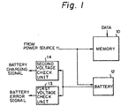
- Figures 1 and 2 are principle structure for explaining the present invention.
- reference number 10 denotes a memory, for example, a non-volatile type memory
- 12 denotes a battery for supplying a voltage when the power source is accidentally interrupted.
- 13 and 14 denote first and second voltage check units for checking the output voltage of the battery 12 (below, battery voltage).
- the first voltage check unit 13 compares the battery voltage with a first reference voltage and generates a battery error signal BERR when the battery voltage is lower than the first reference voltage.
- the second voltage check unit 14 compares the battery voltage with a second reference voltage and generates a battery charging signal BCRG when the battery voltage lies between the first reference voltage and the second reference voltage.
- reference number 2 denotes a control unit for disconnecting the memory 10 from the device controller when the battery charging signal or the battery error signal is input thereto. Further, the control unit 2 informs the battery error state to firmware based on the battery error signal as shown in Fig. 8.
- an external storage device 6 for example, a disk device is directly accessed from a channel system as shown in Fig. 10.
- control unit 2 selectively initiates a write-back mode and a write-through mode. That is, in the write-back mode, the data temporarily stored in the memory 10 is transferred from the device controller to the external storage device 6, and in the write-through mode, the data is directly transferred from the channel system to the external storage device 6 (disk device) not through the memory 10 as shown in Fig. 10.
- the present invention it is possible to easily detect whether the battery is in a deteriorated or insufficient charging state. If the battery is in a deteriorated state, it must be changed to new battery. If the battery is in an insufficient state, the use of the battery is stopped and the write-through mode is initiated between the channel system and the external storage device 6 based on the charging signal.
- FIG. 3 is a schematic block diagram of a data protection system according to an embodiment of the present invention.
- reference number 11 denotes a power source for supplying a voltage Vcc to the memory 10, 15 a timer unit for generating a battery check signal BCK at contact time intervals, 16 a charge circuit for charging the battery 12 from the power source 11, and INV an inverting means.
- RL1 and RL2 denote relays. These relays are closed when the low level signals are input thereto. Accordingly, when the battery check signal BCK is high, the relay RL1 is opened and the relay RL2 is closed. When the battery check signal BCK is low, the relay RL1 is closed and the relay RL2 is opened.
- the relay RL2 when the battery check signal BCK is high, the relay RL2 is closed and the battery voltage V is checked by the first and second voltage check units 13 and 14. Meanwhile, when the battery check signal BCK is low, the relay RL1 is closed and the relay RL2 is opened. Accordingly, the battery 12 is charged from the power source 11 through the relay RL1 and the resistor R.
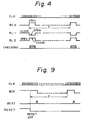
- Figure 4 is a timing chart for explaining a battery checking operation.
- the timer unit 15 operates in response to a clock signal CLK. Accordingly, the timer unit 15 counts the number of clock signals CLK and sets the battery check signal BCK to the high level during a constant time interval T1.
- the battery voltage can be supplied to the memory 10 through the diode D2.
- the first reference voltage V1 is set to 20% of the full charged voltage.
- the second reference voltage V2 is set to 80% of the full charged voltage. Accordingly, when the battery voltage V is lower than the first reference voltage V1, the first voltage check unit 13 generates the battery error signal BERR. In this case, it is necessary to change the battery.
- the second voltage check unit 14 When the battery voltage V lies between the first reference voltage V1 and the second reference voltage V2, the second voltage check unit 14 generates the battery checking signal BCRG. In this case, although the battery is in an insufficient charging state, it is not necessary to change the battery.
- the memory 10 is disconnected from the data transfer route and the transfer mode of the data is changed to the write-through mode in which the external storage device 6 is directly accessed from the channel system. Accordingly, either the battery check signal BERR or the battery charging signal BCRG is generated from the first or second voltage check unit, the memory 10 is disconnected from the device controller, and the transfer mode is changed to the write-through mode. Therefore, it is possible to protect the data stored in the memory 10 in an accidental power OFF which occurs before the data stored in the memory 10 has been transferred to the external storage device 6 (i.e., before the write-back mode). Meanwhile, when the battery is charged over the second reference voltage V2, the battery charging signal BCRG is turned OFF and the memory 10 is again connected to the channel system.
- the data stored in the memory 10 can be securely protected from an accidental power OFF.
- Figure 5 is a schematic block diagram of a device controller, for example, a disk cache system applying the present invention.
- a disk cache system is usually provided between a channel system and an external storage device, and is utilized for increasing the effective performance of the external storage device 6. That is, the disk cache system controls the data transfer between the channel and the external storage device using the cache memory module 3 or without using the cache memory module 3. Accordingly, the disk cache system is a kind of file controller.
- reference 2a denotes a service adaptor constituted by, for example, microprocessor, and provided for supervising each module or each adaptor.
- Reference number 3 denotes a cache memory module constituted by a storage port 3b, memory access controllers (MAC) 30 to 32, a non-volatile memory array (NVTBA) 1, and volatile memories (SSA) 3c to 3d.
- 3a denotes a cache control module for managing the cache memory module 3.
- Reference 2b denotes a resource management adaptor for managing the resources of the whole disk cache system and for controlling connection among adaptors.
- 4a and 4b denotes channel adaptors for connecting a block multiplexer channel (BMC) in the channel system, and for performing an interface control therebetween.
- the block multiplexer channel (BMC) is provided for transferring a plurality of data in a time-sharing operation for each block unit.
- Reference 7 denotes a maintenance module for receiving the battery charging signal BCRG, the battery error signal BERR and the write-back enable signal WBE, and for informing these signals to the service adaptor 2a.
- 8a and 8b denote common buses for connecting the modules 3a, 3, and the adaptors 2a, 2b, 3a, 4a, 4b, 5a and 5b.
- the cache memory module 3 constituted by, for example, the non-volatile type memory array 1 having 16 Mbyte, and DRAM (dynamic random access memory) arrays 3c and 3d each having 256 Mbyte. Each of DRAM's 3c and 3d stores data having a high reference frequency from the data stored in the external storage device 6.
- FIG. 6 is schematic block diagram of the non-volatile type memory array shown in Fig. 5.
- the non-volatile type memory array 1 is constituted by four non-volatile memory cards 1a to 1d, a battery 12, OR gates GT1 and GT2 and a NOR gate GT3.
- the OR gate GT1 receives the battery charging signals +BCRG from each non-volatile memory 1a to 1d and outputs the battery charging signal BCRG.
- the OR gate GT2 receives the battery error signals +BERR from each non-volatile memory 1a to 1d and outputs the battery error signal BERR.
- the NOR gate GT3 receives the battery charging signal BCRG, the battery error signal BERR and the write-through mode signal WTM, and outputs an inverted write enable signal WBE.
- FIG. 7 is a detailed block diagram of the non-volatile type memory card.
- Each non-volatile type memory card 1a to 1d is constituted by a non-volatile memory, the power source 11, the charge circuit 16, the first and second voltage check circuits, and a signal output circuit 17.
- the signal output circuit 17 comprises AND gates G1, G2 and G3, OR gates G4 and G5, a NOR gate G6, flip-flop circuits 17a and 17b, and an inverter IV.
- the AND gate G1 receives the battery check signal and the battery check timing signal BCKT.
- the AND gate G2 receives the battery error signal BERR and the battery check timing signal BCKT.
- the flip-flop circuit 17a sets the battery check signal BCRG and the flip-flop circuit 17b sets the battery error signal BERR.
- the NOR gate G6 receives the reset signal RESET and the write-through mode signal WTM, and sets the flip-flop circuits 17a and 17b to the reset state.
- the transistor Tr of the power source 11 is turned OFF when the power source voltage Vcc falls under 4.2 (v).
- the inverter INV inverts the battery check signal BCK. Accordingly, as explained in Fig. 3, when the battery check signal BCK is high, the relay RL1 is opened and the relay RL2 is closed so that the battery voltage V can be checked by the first and second voltage check units 13 and 14.
- the non-volatile type memory 1 is used as a part of the cache memory module 3. Accordingly, when the cache memory module 3 is not used, the data transfer between the channel and the disk device 6 is performed as follows. This is called "write-through mode" as explained above.
- the write data from the channel is transferred from the BMC (block multiplexer channel) channel to the disk device 6 through the channel adaptor 4a and the device adaptor 5a.
- the data stored in the disk device 6 is read out from the disk device 6 to the BMC channel through the device adaptor 5a and the channel adaptor 4a. This route is shown by a dotted line in Fig. 10.
- the cache memory module 3 is not used in this data transfer route.
- the data having a high reference frequency in the disk device 6 is stored in the cache memory module 3. Accordingly, the write data is transferred from the BMC channel to cache memory module 3 through the channel adaptor 4a and the storage port 3b. At the same time, the write data is transferred to the disk device 6 through the device adaptor 5a. Meanwhile, the read data is transferred from the cache memory module 3 to the BMC channel through the channel adaptor 4a.
- the write data from the BMC channel is stored in the non-volatile type memory 1 and is simultaneously stored in the volatile type memories 3c and 3d.
- the channel adaptor 4a sends a "DEVICE END" signal which indicates completion of the data transfer to the BMC channel.
- the write data stored in the non-volatile type memory 1 is transferred to the disk device 6 through the device adaptor 5a. Accordingly, it is possible to raise the throughput between the channel and the device because the write data is temporarily stored in the non-volatile type memory 1.
- the write data stored in the non-volatile type memory 1 is always written into the disk device 6 through the device adaptor 5a.
- Figure 8 is a flowchart for explaining operation of the structure shown in Figs. 5, 6, and 7, and Figure 9 is a timing chart for explaining a battery checking operation of another embodiment.
- the battery check is performed with two timings, i.e., the timing after the reset state is released and the timing of once per one hour for about 0.45 second.
- the state of the battery voltage is output to the service adaptor 2a through the maintenance module 7, stored in the service adaptor 2a, and informed to the cache control module 3a.
- the resource management adaptor 2b determines either the write-back mode or the write-through mode based on the information of the battery state obtained from the cache control module 3a.
- the commands "RESET OFF" and "WTMSW OFF" are generated from the operation panel in the maintenance module 7. That is, the reset state is released and the write-through mode switch is turned OFF.
- the transfer mode is set to the write-back mode.
- the service adaptor 2a starts the timer unit 15 of the non-volatile type memory 1, sets the battery check signal BCK to the high level during the 0.45 second period.
- the battery voltage is checked by the first and second voltage check units 13 and 14 as explained above during this time interval (TIMER A: OUT).
- step 2 the battery error signal BERR and the battery charging signal BCRG are set in the flip-flop circuits 17a and 17b of the signal output circuit 17 (see, Fig. 7) in synchronization with the battery check timing signal BCKT from the service adaptor 2a.
- the battery error signal +BERR and the battery charging signal +BCRG are transferred to the service adaptor 2a through the OR gates GT1, GT2 and the maintenance module 7 with the write-back enable signal WBE.
- the service adaptor 2a informs these signals to the cache control module 3a.
- the cache control module 3a determines whether or not the battery error signal BERR is valid. When the battery voltage is lower than 20% of the full charge voltage, the cache control module 3a turns ON the write-through mode (WTM ON) and the cache memory module 3 is disconnected from the device controller. Further, "ERROR" is displayed on the operation panel of the maintenance module 7 through the service adaptor 2a. Still further, the cache control module 3a informs the write-through mode to the resource management adaptor 2b.
- the operator can recognize the state of the battery based on the display or the information from the firmware. Further, the operator can change the defect battery to a normal one and the flip-flop circuits 17a and 17b can be returned to the initial state by operating the write-mode switch as a recovery operation.
- step 3 when the battery error is invalid, the cache control module 3a determines whether or not the battery charging signal BCRG is valid.
- the write-through mode is turned OFF (WTM OFF) and the write-back mode is activated since the battery voltage exceeds 80% of the full charge voltage. Further, the display of "CHARGING" of the operation panel is turned OFF (CHARGING OFF).
- step 4 when the battery charging signal BCRG is valid, the cache control module 3a determines the write-through mode (WTM ON) and the cache memory module 3 is disconnected from the device controller. Further, the display of "CHARGING" is turned OFF. If data exists in the non-volatile type memory 1, the cache control module 3a enters an "emergency write-back mode" and commands the cache memory module 3 to transfer the user data to the disk device 6.
- WTM ON write-through mode
- CHARGING is turned OFF. If data exists in the non-volatile type memory 1, the cache control module 3a enters an "emergency write-back mode" and commands the cache memory module 3 to transfer the user data to the disk device 6.
- step 5 the predetermined hour T (one hour) is passed on the timer unit 15 (TIMER B: OUT), the battery check is repeated by the same steps as 1 and 2 .
- the user data stored in the non-volatile type memory 3 is written to the disk device 6 based on the emergency write-back mode when the battery error signal BERR or the battery charging signal BCRG are generated.
- the transfer mode is set to the write-through mode.
- the transfer mode is set to the write-back mode from the operation panel.
- the battery charging signal BCRG is generated, the transfer mode is changed to the write-through mode.
- the transfer mode is automatically set back to the write-back mode.
- the battery check circuit is provided in each non-volatile memory card so that it is possible to check the battery voltage even if one voltage check circuit steps functioning.
Landscapes
- Engineering & Computer Science (AREA)
- Theoretical Computer Science (AREA)
- Physics & Mathematics (AREA)
- General Engineering & Computer Science (AREA)
- General Physics & Mathematics (AREA)
- Power Engineering (AREA)
- Quality & Reliability (AREA)
- Business, Economics & Management (AREA)
- Emergency Management (AREA)
- Techniques For Improving Reliability Of Storages (AREA)
- Power Sources (AREA)
- Memory System Of A Hierarchy Structure (AREA)
Claims (6)
- Système de protection de données destiné à protéger des données temporairement stockées dans une mémoire rémanente (10) prévue dans un régisseur de dispositifs, dans lequel système les données sont stockées de manière permanente dans un dispositif de stockage externe rémanent (6), le système comportantle régisseur de dispositifs ;la mémoire rémanente (10) ;une source d'alimentation électrique (11) destinée à fournir de l'énergie à la mémoire rémanente (10) ;une batterie électrique (12) chargée par la source d'alimentation électrique (11) et fournissant de l'énergie à la mémoire rémanente (10) lorsque la source d'alimentation électrique (11) est interrompue ;un premier moyen (13) de contrôle de tension connecté à la batterie (12), lequel moyen compare la tension de la batterie à une première tension de référence et produit un signal d'erreur de batterie lorsque la tension de la batterie est inférieure à la première tension de référence ; etun deuxième moyen (14) de contrôle de tension connecté à la batterie, lequel moyen compare la tension de la batterie à une deuxième tension de référence, caractérisé en ce que le deuxième moyen (14) de contrôle de tension produit un signal de charge de batterie lorsque la tension de la batterie se situe entre la première tension de référence et la deuxième tension de référence ; et en ce que le régisseur de dispositifs comporte un moyen de commande (2) servant à déconnecter fonctionnellement la mémoire rémanente (10) vis-à-vis du régisseur de dispositifs lorsque le signal de charge de batterie lui est appliqué en entrée.
- Système de protection de données selon la revendication 1, dans lequel le moyen de commande (2) communique une information d'erreur de batterie à un micro-logiciel sur la base du signal d'erreur de batterie.
- Système de protection de données selon la revendication 1, dans lequel le régisseur de dispositifs est connecté entre au moins un système de canaux et le dispositif de stockage externe (6), le régisseur de dispositifs ayant pour fonction de transférer des données ; et le moyen de commande (2) ayant pour fonction de déterminer sélectivement deux modes, un mode étant un mode d'écriture en retour servant à transférer les données du système de canaux au dispositif de stockage externe (6) après que les données ont été stockées dans la mémoire rémanente (10), et l'autre étant un mode d'écriture en direct servant à transférer directement les données du système de canaux au dispositif de stockage externe (6) sans passer par l'intermédiaire de la mémoire rémanente (10) lorsque le signal d'erreur de batterie et, ou bien, le signal de charge de batterie lui sont appliqués en entrée.
- Système de protection de données selon la revendication 3, où le système de protection de données comprend en outre un moyen minuteur (15) servant à délivrer un signal de contrôle de batterie sur la base d'un signal d'horloge prédéterminé.
- Système de protection de données selon la revendication 3 ou 4, où la mémoire rémanente (10) est déconnectée du régisseur de dispositifs dans le mode d'écriture en direct.
- Système de protection de données selon l'une quelconque des revendications précédentes, où un moyen minuteur (15) est fonctionnellement connecté entre les premier et deuxième moyens de contrôle de tension et où un signal de contrôle de batterie est délivré par le moyen minuteur (15) à des intervalles de temps constants.
Applications Claiming Priority (2)
| Application Number | Priority Date | Filing Date | Title |
|---|---|---|---|
| JP118963/88 | 1988-05-16 | ||
| JP63118963A JP2533612B2 (ja) | 1988-05-16 | 1988-05-16 | メモリのデ―タ保護方式 |
Publications (3)
| Publication Number | Publication Date |
|---|---|
| EP0342846A2 EP0342846A2 (fr) | 1989-11-23 |
| EP0342846A3 EP0342846A3 (fr) | 1990-08-22 |
| EP0342846B1 true EP0342846B1 (fr) | 1997-04-09 |
Family
ID=14749611
Family Applications (1)
| Application Number | Title | Priority Date | Filing Date |
|---|---|---|---|
| EP89304682A Expired - Lifetime EP0342846B1 (fr) | 1988-05-16 | 1989-05-09 | Système de protection des données dans un système de traitement de données |
Country Status (7)
| Country | Link |
|---|---|
| US (1) | US5007027A (fr) |
| EP (1) | EP0342846B1 (fr) |
| JP (1) | JP2533612B2 (fr) |
| KR (1) | KR920007378B1 (fr) |
| AU (1) | AU606278B2 (fr) |
| CA (1) | CA1319435C (fr) |
| DE (1) | DE68927941T2 (fr) |
Families Citing this family (44)
| Publication number | Priority date | Publication date | Assignee | Title |
|---|---|---|---|---|
| US5193162A (en) * | 1989-11-06 | 1993-03-09 | Unisys Corporation | Cache memory with data compaction for use in the audit trail of a data processing system having record locking capabilities |
| JPH03182921A (ja) * | 1989-12-11 | 1991-08-08 | Sharp Corp | 電子装置 |
| US5151907A (en) * | 1990-02-20 | 1992-09-29 | Robbins Walter A | Auxiliary power supply for continuation of computer system operation during commercial AC power failure |
| US5345422A (en) * | 1990-07-31 | 1994-09-06 | Texas Instruments Incorporated | Power up detection circuit |
| US5341493A (en) * | 1990-09-21 | 1994-08-23 | Emc Corporation | Disk storage system with write preservation during power failure |
| JPH04178114A (ja) * | 1990-11-09 | 1992-06-25 | Canon Inc | 電子機器 |
| JPH04268990A (ja) * | 1991-02-25 | 1992-09-24 | Fuji Photo Film Co Ltd | メモリカード |
| GB2261753B (en) * | 1991-11-19 | 1995-07-12 | Intel Corp | Multi-mode microprocessor with electrical pin for selective re-initialization of processor state |
| US5428769A (en) * | 1992-03-31 | 1995-06-27 | The Dow Chemical Company | Process control interface system having triply redundant remote field units |
| JP3034741B2 (ja) * | 1993-12-13 | 2000-04-17 | 三菱電機株式会社 | 電源バックアップ装置 |
| US6052789A (en) * | 1994-03-02 | 2000-04-18 | Packard Bell Nec, Inc. | Power management architecture for a reconfigurable write-back cache |
| US5532676A (en) * | 1994-04-29 | 1996-07-02 | Mitel, Inc. | Battery switch for ram backup |
| JP3231561B2 (ja) * | 1994-09-22 | 2001-11-26 | 日本電気株式会社 | バックアップメモリ制御方式 |
| US5604708A (en) * | 1995-01-25 | 1997-02-18 | Dell Usa L.P. | Fail-safe system for preserving a backup battery |
| JP3477689B2 (ja) * | 1995-12-07 | 2003-12-10 | 株式会社日立製作所 | 磁気ディスク制御装置 |
| US5734814A (en) * | 1996-04-15 | 1998-03-31 | Sun Microsystems, Inc. | Host-based RAID-5 and NV-RAM integration |
| US5768208A (en) * | 1996-06-18 | 1998-06-16 | Microchip Technology Incorporated | Fail safe non-volatile memory programming system and method therefor |
| US5784629A (en) * | 1996-09-24 | 1998-07-21 | Apple Computer, Inc. | System and method for conserving power within a backup battery device |
| US5973734A (en) | 1997-07-09 | 1999-10-26 | Flashpoint Technology, Inc. | Method and apparatus for correcting aspect ratio in a camera graphical user interface |
| JP4231572B2 (ja) * | 1998-07-07 | 2009-03-04 | 沖電気工業株式会社 | 電圧監視回路及びそれを内蔵したメモリカード |
| FR2785693B1 (fr) * | 1998-11-06 | 2000-12-15 | Bull Sa | Dispositif et procede de cache disque securise en ecriture pour disques durs de sous-systeme a memoire de masse |
| US6317141B1 (en) * | 1998-12-31 | 2001-11-13 | Flashpoint Technology, Inc. | Method and apparatus for editing heterogeneous media objects in a digital imaging device |
| CN100343786C (zh) * | 2000-12-26 | 2007-10-17 | 神基科技股份有限公司 | 电源监控保护方法 |
| US6580650B2 (en) | 2001-03-16 | 2003-06-17 | International Business Machines Corporation | DRAM word line voltage control to insure full cell writeback level |
| KR20020062262A (ko) * | 2002-07-02 | 2002-07-25 | (주)한창트랜스 | 무정전전원공급장치 |
| JP2005115771A (ja) * | 2003-10-09 | 2005-04-28 | Hitachi Ltd | ディスクアレイ装置 |
| US7436151B2 (en) * | 2004-12-23 | 2008-10-14 | Dell Products L.P. | Systems and methods for detecting charge switching element failure in a battery system |
| US7518341B2 (en) * | 2004-12-23 | 2009-04-14 | Dell Product L.P. | Method for verifying smart battery failures by measuring input charging voltage and associated systems |
| JP4836647B2 (ja) * | 2006-04-21 | 2011-12-14 | 株式会社東芝 | 不揮発性キャッシュメモリを用いる記憶装置とその制御方法 |
| US9224145B1 (en) | 2006-08-30 | 2015-12-29 | Qurio Holdings, Inc. | Venue based digital rights using capture device with digital watermarking capability |
| WO2008056593A1 (fr) * | 2006-11-06 | 2008-05-15 | Panasonic Corporation | Dispositif d'enregistrement |
| JP2009152703A (ja) * | 2007-12-19 | 2009-07-09 | Konica Minolta Business Technologies Inc | 画像処理装置 |
| CN101620878A (zh) * | 2008-07-03 | 2010-01-06 | 鸿富锦精密工业(深圳)有限公司 | 存储系统 |
| JP5514364B2 (ja) | 2010-08-27 | 2014-06-04 | 株式会社日立製作所 | 記憶制御装置及び記憶制御装置の動作モード制御方法 |
| DE102011052533B4 (de) * | 2011-08-09 | 2015-02-26 | Esw Gmbh | Schaltungsanordnung zum Schutz von Speicherinhalten |
| WO2013054374A1 (fr) * | 2011-10-12 | 2013-04-18 | Hitachi, Ltd. | Système de stockage, et procédé de sauvegarde de données et procédé de redémarrage de système de stockage |
| US10025711B2 (en) * | 2012-01-16 | 2018-07-17 | Qualcomm Incorporated | Hybrid write-through/write-back cache policy managers, and related systems and methods |
| JP5996228B2 (ja) * | 2012-03-26 | 2016-09-21 | 株式会社ダイヘン | ロボット制御装置 |
| IL236627A0 (en) * | 2015-01-11 | 2015-04-30 | Storone Ltd | Method and system for controlling volatile memory |
| JP6536160B2 (ja) * | 2015-04-30 | 2019-07-03 | 富士通株式会社 | ストレージシステム、制御装置および制御プログラム |
| JP6348099B2 (ja) * | 2015-12-02 | 2018-06-27 | ファナック株式会社 | 同期運転教示データ作成時の確認手段を備える制御装置 |
| CN108711440B (zh) * | 2018-08-02 | 2024-04-30 | 珠海格力电器股份有限公司 | 写保护电路和写保护方法、写保护装置及电器设备 |
| US11659058B2 (en) | 2019-06-28 | 2023-05-23 | Amazon Technologies, Inc. | Provider network connectivity management for provider network substrate extensions |
| US11044118B1 (en) * | 2019-06-28 | 2021-06-22 | Amazon Technologies, Inc. | Data caching in provider network substrate extensions |
Family Cites Families (11)
| Publication number | Priority date | Publication date | Assignee | Title |
|---|---|---|---|---|
| JPS5610871U (fr) * | 1979-07-04 | 1981-01-29 | ||
| JPS56103722A (en) * | 1980-01-19 | 1981-08-19 | Tokico Ltd | Failure detector of battery for memory in console device |
| JPS58146099A (ja) * | 1982-02-24 | 1983-08-31 | Hitachi Ltd | メモリ保護装置 |
| US4506323A (en) * | 1982-03-03 | 1985-03-19 | Sperry Corporation | Cache/disk file status indicator with data protection feature |
| US4547629A (en) * | 1984-02-06 | 1985-10-15 | Comdial Technology Corporation | Energy management circuit |
| US4654778A (en) * | 1984-06-27 | 1987-03-31 | International Business Machines Corporation | Direct parallel path for storage accesses unloading common system path |
| JPS61147357A (ja) * | 1984-12-21 | 1986-07-05 | Casio Comput Co Ltd | デ−タ処理装置 |
| US4777626A (en) * | 1984-12-22 | 1988-10-11 | Tokyo Electric Co., Ltd. | Memory device having backup power supply |
| JPS628212A (ja) * | 1985-07-04 | 1987-01-16 | Nec Corp | バツテリ−電圧検出回路 |
| US4707618A (en) * | 1986-06-02 | 1987-11-17 | Haas Richard M | Switch protection mechanism |
| JPS635539U (fr) * | 1986-06-25 | 1988-01-14 |
-
1988
- 1988-05-16 JP JP63118963A patent/JP2533612B2/ja not_active Expired - Fee Related
-
1989
- 1989-05-03 CA CA000598645A patent/CA1319435C/fr not_active Expired - Fee Related
- 1989-05-08 AU AU34085/89A patent/AU606278B2/en not_active Ceased
- 1989-05-09 US US07/349,310 patent/US5007027A/en not_active Expired - Lifetime
- 1989-05-09 DE DE68927941T patent/DE68927941T2/de not_active Expired - Fee Related
- 1989-05-09 EP EP89304682A patent/EP0342846B1/fr not_active Expired - Lifetime
- 1989-05-16 KR KR1019890006497A patent/KR920007378B1/ko not_active IP Right Cessation
Also Published As
| Publication number | Publication date |
|---|---|
| US5007027A (en) | 1991-04-09 |
| JP2533612B2 (ja) | 1996-09-11 |
| EP0342846A3 (fr) | 1990-08-22 |
| JPH01288948A (ja) | 1989-11-21 |
| DE68927941T2 (de) | 1997-08-14 |
| DE68927941D1 (de) | 1997-05-15 |
| CA1319435C (fr) | 1993-06-22 |
| AU3408589A (en) | 1989-12-14 |
| KR920007378B1 (ko) | 1992-08-31 |
| EP0342846A2 (fr) | 1989-11-23 |
| KR900019306A (ko) | 1990-12-24 |
| AU606278B2 (en) | 1991-01-31 |
Similar Documents
| Publication | Publication Date | Title |
|---|---|---|
| EP0342846B1 (fr) | Système de protection des données dans un système de traitement de données | |
| US5414861A (en) | Data protection system using different levels of reserve power to maintain data in volatile memories for any period of time | |
| US5204963A (en) | Method and apparatus for a backup power controller for volatile random access memory | |
| EP0116344B1 (fr) | Système de mémoire doublé à alimentation de secours | |
| US7131013B2 (en) | Power supply control system and storage device for holding data just prior to the occurence of an error | |
| JP3477689B2 (ja) | 磁気ディスク制御装置 | |
| US5640357A (en) | Storage device using dynamic RAM | |
| US5005172A (en) | Diagnostic system in a data processing system | |
| US6480933B1 (en) | Disk cache device and method for secure writing of hard disks in mass memory subsystems | |
| US5237687A (en) | Microprogram load unit having alternative backup memory sources | |
| US5408421A (en) | Portable battery back-up data cartridge | |
| WO2000067126A1 (fr) | Procede et dispositif de reintegration automatique d'un module dans un systeme informatique | |
| EP0626647B1 (fr) | Dispositif de copie pour effectuer une opération de copie entre un système de traitement actif et un système de traitement au repos | |
| JP3082525B2 (ja) | 制御装置 | |
| US20030221058A1 (en) | Mirrored computer memory on single bus | |
| JPH08220198A (ja) | 電池バックアップメモリユニットおよびバックアップ機能試験方法 | |
| JP3124201B2 (ja) | 入出力制御装置 | |
| JP2782784B2 (ja) | マイクロコンピュータの制御装置 | |
| JPH08140287A (ja) | メモリバックアップ制御装置 | |
| JPH04289558A (ja) | ディスク装置における電源瞬断時の書き込みデータ保護方式 | |
| SU1129615A1 (ru) | Устройство дл контрол данных электронной вычислительной машины при прерывани х питани | |
| JPH06348604A (ja) | メモリコピー方式 | |
| JPS60138624A (ja) | バツテリバツクアツプしたramを有する制御装置 | |
| JPH0683720A (ja) | データバックアップ式コンピュータシステム | |
| JPH01196688A (ja) | 車種データ処理装置 |
Legal Events
| Date | Code | Title | Description |
|---|---|---|---|
| PUAI | Public reference made under article 153(3) epc to a published international application that has entered the european phase |
Free format text: ORIGINAL CODE: 0009012 |
|
| AK | Designated contracting states |
Kind code of ref document: A2 Designated state(s): DE FR GB IT NL |
|
| PUAL | Search report despatched |
Free format text: ORIGINAL CODE: 0009013 |
|
| AK | Designated contracting states |
Kind code of ref document: A3 Designated state(s): DE FR GB IT NL |
|
| 17P | Request for examination filed |
Effective date: 19901129 |
|
| 17Q | First examination report despatched |
Effective date: 19930913 |
|
| GRAG | Despatch of communication of intention to grant |
Free format text: ORIGINAL CODE: EPIDOS AGRA |
|
| GRAH | Despatch of communication of intention to grant a patent |
Free format text: ORIGINAL CODE: EPIDOS IGRA |
|
| GRAH | Despatch of communication of intention to grant a patent |
Free format text: ORIGINAL CODE: EPIDOS IGRA |
|
| GRAA | (expected) grant |
Free format text: ORIGINAL CODE: 0009210 |
|
| AK | Designated contracting states |
Kind code of ref document: B1 Designated state(s): DE FR GB IT NL |
|
| PG25 | Lapsed in a contracting state [announced via postgrant information from national office to epo] |
Ref country code: IT Free format text: LAPSE BECAUSE OF FAILURE TO SUBMIT A TRANSLATION OF THE DESCRIPTION OR TO PAY THE FEE WITHIN THE PRE;WARNING: LAPSES OF ITALIAN PATENTS WITH EFFECTIVE DATE BEFORE 2007 MAY HAVE OCCURRED AT ANY TIME BEFORE 2007. THE CORRECT EFFECTIVE DATE MAY BE DIFFERENT FROM THE ONE RECORDED.SCRIBED TIME-LIMIT Effective date: 19970409 Ref country code: NL Effective date: 19970409 Ref country code: FR Effective date: 19970409 |
|
| REF | Corresponds to: |
Ref document number: 68927941 Country of ref document: DE Date of ref document: 19970515 |
|
| NLV1 | Nl: lapsed or annulled due to failure to fulfill the requirements of art. 29p and 29m of the patents act | ||
| EN | Fr: translation not filed | ||
| PLBE | No opposition filed within time limit |
Free format text: ORIGINAL CODE: 0009261 |
|
| STAA | Information on the status of an ep patent application or granted ep patent |
Free format text: STATUS: NO OPPOSITION FILED WITHIN TIME LIMIT |
|
| 26N | No opposition filed | ||
| REG | Reference to a national code |
Ref country code: GB Ref legal event code: IF02 |
|
| PGFP | Annual fee paid to national office [announced via postgrant information from national office to epo] |
Ref country code: GB Payment date: 20050504 Year of fee payment: 17 |
|
| PGFP | Annual fee paid to national office [announced via postgrant information from national office to epo] |
Ref country code: DE Payment date: 20050506 Year of fee payment: 17 |
|
| PG25 | Lapsed in a contracting state [announced via postgrant information from national office to epo] |
Ref country code: GB Free format text: LAPSE BECAUSE OF NON-PAYMENT OF DUE FEES Effective date: 20060509 |
|
| PG25 | Lapsed in a contracting state [announced via postgrant information from national office to epo] |
Ref country code: DE Free format text: LAPSE BECAUSE OF NON-PAYMENT OF DUE FEES Effective date: 20061201 |
|
| GBPC | Gb: european patent ceased through non-payment of renewal fee |
Effective date: 20060509 |