EP0341034A2 - Herstellungsverfahren von Halbleitervorrichtungen - Google Patents
Herstellungsverfahren von Halbleitervorrichtungen Download PDFInfo
- Publication number
- EP0341034A2 EP0341034A2 EP89304433A EP89304433A EP0341034A2 EP 0341034 A2 EP0341034 A2 EP 0341034A2 EP 89304433 A EP89304433 A EP 89304433A EP 89304433 A EP89304433 A EP 89304433A EP 0341034 A2 EP0341034 A2 EP 0341034A2
- Authority
- EP
- European Patent Office
- Prior art keywords
- semiconductor
- substrate
- semiconductor devices
- production
- plane
- Prior art date
- Legal status (The legal status is an assumption and is not a legal conclusion. Google has not performed a legal analysis and makes no representation as to the accuracy of the status listed.)
- Granted
Links
Images

Classifications
-
- H—ELECTRICITY
- H10—SEMICONDUCTOR DEVICES; ELECTRIC SOLID-STATE DEVICES NOT OTHERWISE PROVIDED FOR
- H10H—INORGANIC LIGHT-EMITTING SEMICONDUCTOR DEVICES HAVING POTENTIAL BARRIERS
- H10H20/00—Individual inorganic light-emitting semiconductor devices having potential barriers, e.g. light-emitting diodes [LED]
- H10H20/01—Manufacture or treatment
- H10H20/011—Manufacture or treatment of bodies, e.g. forming semiconductor layers
- H10H20/013—Manufacture or treatment of bodies, e.g. forming semiconductor layers having light-emitting regions comprising only Group III-V materials
-
- H—ELECTRICITY
- H01—ELECTRIC ELEMENTS
- H01S—DEVICES USING THE PROCESS OF LIGHT AMPLIFICATION BY STIMULATED EMISSION OF RADIATION [LASER] TO AMPLIFY OR GENERATE LIGHT; DEVICES USING STIMULATED EMISSION OF ELECTROMAGNETIC RADIATION IN WAVE RANGES OTHER THAN OPTICAL
- H01S5/00—Semiconductor lasers
- H01S5/02—Structural details or components not essential to laser action
- H01S5/0201—Separation of the wafer into individual elements, e.g. by dicing, cleaving, etching or directly during growth
-
- H10P54/00—
-
- H—ELECTRICITY
- H01—ELECTRIC ELEMENTS
- H01S—DEVICES USING THE PROCESS OF LIGHT AMPLIFICATION BY STIMULATED EMISSION OF RADIATION [LASER] TO AMPLIFY OR GENERATE LIGHT; DEVICES USING STIMULATED EMISSION OF ELECTROMAGNETIC RADIATION IN WAVE RANGES OTHER THAN OPTICAL
- H01S5/00—Semiconductor lasers
- H01S5/02—Structural details or components not essential to laser action
- H01S5/0201—Separation of the wafer into individual elements, e.g. by dicing, cleaving, etching or directly during growth
- H01S5/0202—Cleaving
Definitions
- This invention relates to a method for the production of semiconductor devices, and more particularly, it relates to a method for the production of semiconductor devices by dividing a semiconductor wafer in which the semiconductor devices are formed on a semiconductor substrate, the growth plane of which is substantially the (111) plane.
- various semiconductor laser devices which are included in semiconductor devices, have a resonator structure that is formed with the use of cleavage planes of the semiconductor crystal used as a substrate.
- Such semiconductor laser devices are usually produced according to the process as shown in Figures 2a to 2c.
- a multi-layered structure comprising a plurality of epitaxial layers is grown on the (100) plane of a substrate that is made of a zinc blende-type semiconductor crystal.
- the resulting semiconductor wafer, in which the semiconductor laser devices are formed on the substrate, is cleaved in several small bars 31 .
- the small bar 31 is provided with partition patterns 33 on the upper surface thereof and parallel scratches 34 are formed between the adjacent partition patterns 33 by means of a diamond scriber 35 .
- the direction of these scratches 34 is normal to the cleavage plane 32 of the small bar 31 .
- a plurality of the small bars 31 are attached to the upper surface of an adhesive sheet 36 parallel to each other.
- the adhesive sheet 36 is stretched in longitudinal and transverse directions with the application of even force.
- the strength against the stretch of the portions containing the scratch 34 formed on the upper face of the small bar 31 is lower than of other portions and the direction of the scratch 34 corresponds to that of easy cleavage of the semiconductor substrate. Therefore, when the adhesive sheet 36 is stretched in longitudinal and transverse directions, each small bar 31 is readily divided at each portion containing the scratch 34 to separate semiconductor laser devices 37 .
- conventional semiconductor laser devices are produced from a semiconductor wafer in which a multi-layered structure comprising a plurality of epitaxial layers are grown on a substrate made of a zinc blende-type semiconductor crystal, the growth plane of said substrate being substantially the (100) plane.
- the ⁇ 011> direction of easy cleavage of the semiconductor substrate is always normal to the cleavage plane 32 of the small bar 31 , so that if scratches 34 are formed in the direction of easy cleavage that is normal to the cleavage plane 32 , the small bar 31 can readily be divided in the same way as mentioned above, resulting in the semiconductor laser devices 37 separated in a rectangular shape.
- semiconductor laser devices formed on the (111) plane of a semiconductor substrate have excellent device characteristics which are significantly improved as compared with conventional semiconductor laser devices (see, for example, T. Hayakawa et al., Japanese Journal of Applied Physics, vol. 26, L302 (1987); U.S. Patent Application Serial Nos. 159,797 and 031,678).
- the semiconductor wafer produced using such a semiconductor substrate is divided into chips, if the facets 21 for the emission of laser light correspond to the (011) cleavage planes, the direction of scratches formed by means of a diamond scriber does not correspond to that of easy cleavage of the semiconductor substrate. That is, the direction of the scratches intersects the direction of easy cleavage.
- small bars are divided into semiconductor laser devices 25 with extremely irregular shapes as shown in Figure 3b.
- the semiconductor laser devices 25 are produced in the form of parallelograms, as shown in Figure 3c, or trapezoids. In such a case, unnecessary portions 25a having large areas may be formed in the semiconductor laser device 25 , which decreases the number of devices that can be made from any given wafer.
- the method for the production of semiconductor devices of this invention comprises the steps of growing a multi-layered structure comprising a plurality of epitaxial layers on a semiconductor substrate, resulting in a semiconductor wafer in which the semiconductor devices are formed on the substrate; forming striped grooves on the back face of the substrate, each of the striped grooves being positioned between the adjacent semiconductor devices; and dividing the semiconductor wafer along the striped grooves to separate the semiconductor devices.
- the striped grooves are formed in a direction which is different from that of easy cleavage of the substrate.
- the substrate is made of a zinc blende-type semiconductor crystal, the growth plane thereof being substantially the (111) plane.
- the striped grooves are formed by an etching technique.
- the multi-layered structure comprises an optical waveguide to form a semiconductor laser device.
- the substrate is made of a zinc blende-type semiconductor crystal, the growth plane thereof being substantially the (111) plane.
- the striped grooves are formed parallel to the optical waveguide.
- the invention described herein makes possible the objective of providing a method for the production of semiconductor devices, in which even when the direction of easy cleavage of the semiconductor substrate used intersects the direction of division of the resulting semiconductor wafer (e.g., even when a semiconductor substrate, the growth plane of which is substantially the (111) plane, is used to form the semiconductor wafer), high-quality semiconductor devices can be produced in a uniform rectangular shape without incurring structural damage and without degrading the device characteristics with wafer dust, thereby attaining high productivity.
- This invention provides a method for the production of semiconductor devices by dividing a semiconductor wafer in which the semiconductor devices are formed on a semiconductor substrate.
- This method comprises the step of forming striped grooves on the back face of the substrate in the direction which is different from that of easy cleavage of the substrate.
- the thickness of the wafer at the striped grooves is lower than that of the other portion, so that the strength of the wafer at the striped grooves can be decreased significantly as compared with that of the other portion. Therefore, with the use of these striped grooves, the semiconductor wafer can readily be cleaved in a straight form at the portions other than the cleavage planes of a semiconductor crystal that is used for the substrate, resulting in semiconductor devices with a uniform rectangular shape.
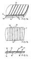
- Figures 1a to 1c show the process for the production of semiconductor laser devices with the use of a semiconductor substrate, the growth plane of which is the (111)B plane, according to this invention.
- a multi-layered structure 12 constituting a GRIN-SCH (graded-index separate confinement heterostructure) semiconductor laser with a single quantum well structure is grown by molecular beam epitaxy (MBE).
- MBE molecular beam epitaxy
- a SiNx current blocking layer 13 is formed by plasma chemical vapor deposition (plasma CVD).
- plasma CVD plasma chemical vapor deposition
- striped channels 15 having a width of 50 ⁇ m are formed by photolithography and etching techniques, resulting in a striped structure within which current is confined.
- the striped channels 15 are parallel to each other and normal to the cleavage plane 14 of a GaAs crystal used for the substrate 11 . Then, the upper face of the current blocking layer 13 including the striped channels 15 is subjected to a vapor deposition treatment with a material of AuZn to form a p-sided electrode. Thereafter, the back face of the n-GaAs substrate is rubbed down, resulting in a semiconductor laser wafer having a thickness of 100 ⁇ m.
- striped grooves 16 for dividing the wafer are formed in the back face of the n-GaAs substrate 11 of the semiconductor laser wafer obtained.
- the position of each of the striped grooves 16 is set to be parallel to and approximately in the middle of the two adjacent striped channels 15 .
- the etchant used for wet etching is a mixture of H2SO4, H2O2, and H2O in the proportions of 1:2:50.
- the width and depth of the striped grooves 16 were 10 ⁇ m and 5 ⁇ m, respectively.
- an n-sided electrode of AuGe is disposed by the vapor deposition method, followed by forming aluminum patterns 18 on the surface of the n-sided electrode.
- the aluminum patterns 18 serve as markers in dividing the wafer.
- the semiconductor laser wafer is then cleaved with the use of a set of cleavage planes 14 to form a laser resonator, resulting in small bars 17 .
- the cleavage planes 14 are normal to the ⁇ 011> direction of the n-GaAs substrate 11 .
- high-quality semiconductor laser devices can be produced without incurring structural damage in their optical waveguides and without wafer dust adhering to the facets used for the emission of laser light.
- the striped grooves 16 are formed on the back face of the substrate 11 by a wet etching technique using a sulfuric acid-containing etchant, a dry etching technique such as reactive ion beam etching (RIBE) and the like can also be used to form the striped grooves 16 .
- a dry etching technique such as reactive ion beam etching (RIBE) and the like can also be used to form the striped grooves 16 .
- the striped grooves 16 for dividing the small bar into the semiconductor devices may also be in the discrete form.
- the size of the striped grooves 16 such as their depth, width, and length, can be conveniently determined depending upon the size of the semiconductor wafers, such as its thickness.
- the sequence of the steps of forming the striped grooves 16 on the back face of the substrate 11 ; growing a multi-layered structure 12 on the substrate 11 ; and providing the striped channels 15 on the upper face of the semiconductor wafer can be altered. If the back face of the substrate 11 is not rubbed down, after the striped grooves 16 are formed on this face, the multi-layered structure 12 may be grown on the upper face of the substrate 11 , followed by providing the striped channels 15 to complete the semiconductor wafer.
- the growth plane of the semiconductor substrate 11 is substantially the (111) plane.
- the angle at which the growth plane of the substrate 11 is inclined to the (111) plane is preferably within ⁇ 5 degrees.
Landscapes
- Physics & Mathematics (AREA)
- Condensed Matter Physics & Semiconductors (AREA)
- General Physics & Mathematics (AREA)
- Electromagnetism (AREA)
- Optics & Photonics (AREA)
- Semiconductor Lasers (AREA)
- Dicing (AREA)
Applications Claiming Priority (2)
| Application Number | Priority Date | Filing Date | Title |
|---|---|---|---|
| JP110964/88 | 1988-05-06 | ||
| JP63110964A JPH01280388A (ja) | 1988-05-06 | 1988-05-06 | 半導体素子の製造方法 |
Publications (3)
| Publication Number | Publication Date |
|---|---|
| EP0341034A2 true EP0341034A2 (de) | 1989-11-08 |
| EP0341034A3 EP0341034A3 (en) | 1990-08-22 |
| EP0341034B1 EP0341034B1 (de) | 1993-11-24 |
Family
ID=14548978
Family Applications (1)
| Application Number | Title | Priority Date | Filing Date |
|---|---|---|---|
| EP19890304433 Expired - Lifetime EP0341034B1 (de) | 1988-05-06 | 1989-05-03 | Herstellungsverfahren von Halbleitervorrichtungen |
Country Status (3)
| Country | Link |
|---|---|
| EP (1) | EP0341034B1 (de) |
| JP (1) | JPH01280388A (de) |
| DE (1) | DE68910873T2 (de) |
Cited By (3)
| Publication number | Priority date | Publication date | Assignee | Title |
|---|---|---|---|---|
| EP0617490A3 (de) * | 1993-03-22 | 1994-12-21 | Mitsubishi Electric Corp | Scheibe mit Halbleiterlasern und Verfahren zum Spalten einer solchen Scheibe. |
| WO2014195488A1 (en) * | 2013-06-07 | 2014-12-11 | Siemens Aktiengesellschaft | Radiation detector manufactured by dicing a semiconductor wafer and dicing method therefor |
| WO2019137816A1 (de) * | 2018-01-15 | 2019-07-18 | Osram Opto Semiconductors Gmbh | Verfahren zum vereinzeln von halbleiterbauteilen und halbleiterbauteil |
Families Citing this family (3)
| Publication number | Priority date | Publication date | Assignee | Title |
|---|---|---|---|---|
| JP4776478B2 (ja) * | 2006-09-06 | 2011-09-21 | 東芝ディスクリートテクノロジー株式会社 | 化合物半導体素子及びその製造方法 |
| JP4573863B2 (ja) * | 2006-11-30 | 2010-11-04 | 三洋電機株式会社 | 窒化物系半導体素子の製造方法 |
| CN115332944B (zh) * | 2022-08-22 | 2023-12-26 | 武汉云岭光电股份有限公司 | 一种半导体激光器制备方法 |
Family Cites Families (2)
| Publication number | Priority date | Publication date | Assignee | Title |
|---|---|---|---|---|
| CA1140661A (en) * | 1978-10-13 | 1983-02-01 | Geoffrey R. Woolhouse | Method of cleaving semiconductor diode laser wafers |
| CA1201520A (en) * | 1982-09-10 | 1986-03-04 | Charles A. Burrus, Jr. | Fabrication of cleaved semiconductor lasers |
-
1988
- 1988-05-06 JP JP63110964A patent/JPH01280388A/ja active Pending
-
1989
- 1989-05-03 EP EP19890304433 patent/EP0341034B1/de not_active Expired - Lifetime
- 1989-05-03 DE DE89304433T patent/DE68910873T2/de not_active Expired - Fee Related
Cited By (6)
| Publication number | Priority date | Publication date | Assignee | Title |
|---|---|---|---|---|
| EP0617490A3 (de) * | 1993-03-22 | 1994-12-21 | Mitsubishi Electric Corp | Scheibe mit Halbleiterlasern und Verfahren zum Spalten einer solchen Scheibe. |
| US5418799A (en) * | 1993-03-22 | 1995-05-23 | Mitsubishi Denki Kabushiki Kaisha | Semiconductor laser element structure |
| WO2014195488A1 (en) * | 2013-06-07 | 2014-12-11 | Siemens Aktiengesellschaft | Radiation detector manufactured by dicing a semiconductor wafer and dicing method therefor |
| US9755098B2 (en) | 2013-06-07 | 2017-09-05 | Siemens Aktiengesellschaft | Radiation detector manufactured by dicing a semiconductor wafer and dicing method therefor |
| WO2019137816A1 (de) * | 2018-01-15 | 2019-07-18 | Osram Opto Semiconductors Gmbh | Verfahren zum vereinzeln von halbleiterbauteilen und halbleiterbauteil |
| US11837844B2 (en) | 2018-01-15 | 2023-12-05 | Osram Oled Gmbh | Method for manufacturing optoelectric semiconductor component and optoelectric semiconductor component device |
Also Published As
| Publication number | Publication date |
|---|---|
| DE68910873T2 (de) | 1994-03-17 |
| DE68910873D1 (de) | 1994-01-05 |
| JPH01280388A (ja) | 1989-11-10 |
| EP0341034B1 (de) | 1993-11-24 |
| EP0341034A3 (en) | 1990-08-22 |
Similar Documents
| Publication | Publication Date | Title |
|---|---|---|
| US5313484A (en) | Quantum box or quantum wire semiconductor structure and methods of producing same | |
| EP0800244B1 (de) | Herstellungsverfahren für III/V Halbleiterlaser | |
| EP0506453B1 (de) | Quanten-Faden-Struktur und Methode zu deren Herstellung | |
| EP1780748B1 (de) | Gruppe III-Nitridschichten mit strukturierten Oberflächen | |
| EP0547694B1 (de) | Verfahren zur Herstellung einer optoelektronischen Halbleiteranordnung, wobei ein Halbleiterkörper mit einer obersten Schicht aus GaAs und einer darunter liegenden, InP enthaltenden Schicht in einem in SiCl4 und Ar erzeugten Plasma geätzt wird | |
| KR960043369A (ko) | 반도체 레이저 장치 및 그의 제조방법 | |
| JPS62194691A (ja) | 光導波路領域を有する半導体光集積装置の製造方法 | |
| CA2026289A1 (en) | Method of manufacturing semiconductor laser | |
| EP0341034A2 (de) | Herstellungsverfahren von Halbleitervorrichtungen | |
| US4862472A (en) | Semiconductor laser device | |
| JP2836822B2 (ja) | 導波路型半導体光素子の製造方法 | |
| JP2960926B2 (ja) | レーザダイオードの製造方法 | |
| Dzurko et al. | MOCVD growth of AlGaAs/GaAs structures on nonplanar {111} substrates: Evidence for lateral gas phase diffusion | |
| JP2000133871A (ja) | 半導体レーザ素子の製造方法 | |
| JPH05315703A (ja) | 半導体レーザの製造方法 | |
| KR100546572B1 (ko) | 레이저 다이오드 제조방법 | |
| JPH01175281A (ja) | 半導体レーザアレイ装置 | |
| JPS63196089A (ja) | 半導体発光素子の製造方法 | |
| KR0141254B1 (ko) | 반도체 레이저장치의 제조방법 | |
| JPH07193322A (ja) | 半導体レーザアレイの製造方法 | |
| JPH02119285A (ja) | 半導体レーザの製造方法 | |
| CA1181670A (en) | Method of preferentially etching optically flat mirror facets in ingaasp/inp heterostructures | |
| JPS6439789A (en) | Manufacture of resonator for semiconductor laser | |
| Gotoda et al. | Fabrication of smooth facets of InP by selective sidewall epitaxy using CBE | |
| JP3128987B2 (ja) | 半導体結晶面の作製方法及び半導体結晶面より成る反射鏡及び半導体量子構造 |
Legal Events
| Date | Code | Title | Description |
|---|---|---|---|
| PUAI | Public reference made under article 153(3) epc to a published international application that has entered the european phase |
Free format text: ORIGINAL CODE: 0009012 |
|
| 17P | Request for examination filed |
Effective date: 19890526 |
|
| AK | Designated contracting states |
Kind code of ref document: A2 Designated state(s): DE FR GB |
|
| PUAL | Search report despatched |
Free format text: ORIGINAL CODE: 0009013 |
|
| AK | Designated contracting states |
Kind code of ref document: A3 Designated state(s): DE FR GB |
|
| 17Q | First examination report despatched |
Effective date: 19920807 |
|
| GRAA | (expected) grant |
Free format text: ORIGINAL CODE: 0009210 |
|
| AK | Designated contracting states |
Kind code of ref document: B1 Designated state(s): DE FR GB |
|
| ET | Fr: translation filed | ||
| REF | Corresponds to: |
Ref document number: 68910873 Country of ref document: DE Date of ref document: 19940105 |
|
| RIN2 | Information on inventor provided after grant (corrected) |
Free format text: HOSODA, MASAHIRO * KONDO, MASAFUMI * SUYAMA, TAKAHIRO * SASAKI, KAZUAKI * TAKAHASHI, KOSEI * HAYAKAWA, TOSHIRO |
|
| PLBE | No opposition filed within time limit |
Free format text: ORIGINAL CODE: 0009261 |
|
| STAA | Information on the status of an ep patent application or granted ep patent |
Free format text: STATUS: NO OPPOSITION FILED WITHIN TIME LIMIT |
|
| 26N | No opposition filed | ||
| REG | Reference to a national code |
Ref country code: GB Ref legal event code: IF02 |
|
| PGFP | Annual fee paid to national office [announced via postgrant information from national office to epo] |
Ref country code: GB Payment date: 20040428 Year of fee payment: 16 |
|
| PGFP | Annual fee paid to national office [announced via postgrant information from national office to epo] |
Ref country code: FR Payment date: 20040510 Year of fee payment: 16 |
|
| PGFP | Annual fee paid to national office [announced via postgrant information from national office to epo] |
Ref country code: DE Payment date: 20040513 Year of fee payment: 16 |
|
| PG25 | Lapsed in a contracting state [announced via postgrant information from national office to epo] |
Ref country code: GB Free format text: LAPSE BECAUSE OF NON-PAYMENT OF DUE FEES Effective date: 20050503 |
|
| PG25 | Lapsed in a contracting state [announced via postgrant information from national office to epo] |
Ref country code: DE Free format text: LAPSE BECAUSE OF NON-PAYMENT OF DUE FEES Effective date: 20051201 |
|
| GBPC | Gb: european patent ceased through non-payment of renewal fee |
Effective date: 20050503 |
|
| PG25 | Lapsed in a contracting state [announced via postgrant information from national office to epo] |
Ref country code: FR Free format text: LAPSE BECAUSE OF NON-PAYMENT OF DUE FEES Effective date: 20060131 |
|
| REG | Reference to a national code |
Ref country code: FR Ref legal event code: ST Effective date: 20060131 |