EP0338840B1 - Optical pick-up device - Google Patents
Optical pick-up device Download PDFInfo
- Publication number
- EP0338840B1 EP0338840B1 EP89303962A EP89303962A EP0338840B1 EP 0338840 B1 EP0338840 B1 EP 0338840B1 EP 89303962 A EP89303962 A EP 89303962A EP 89303962 A EP89303962 A EP 89303962A EP 0338840 B1 EP0338840 B1 EP 0338840B1
- Authority
- EP
- European Patent Office
- Prior art keywords
- photo
- detecting
- sub
- recording medium
- diffracting
- Prior art date
- Legal status (The legal status is an assumption and is not a legal conclusion. Google has not performed a legal analysis and makes no representation as to the accuracy of the status listed.)
- Expired - Lifetime
Links
Images


Classifications
-
- G—PHYSICS
- G11—INFORMATION STORAGE
- G11B—INFORMATION STORAGE BASED ON RELATIVE MOVEMENT BETWEEN RECORD CARRIER AND TRANSDUCER
- G11B7/00—Recording or reproducing by optical means, e.g. recording using a thermal beam of optical radiation by modifying optical properties or the physical structure, reproducing using an optical beam at lower power by sensing optical properties; Record carriers therefor
- G11B7/08—Disposition or mounting of heads or light sources relatively to record carriers
- G11B7/09—Disposition or mounting of heads or light sources relatively to record carriers with provision for moving the light beam or focus plane for the purpose of maintaining alignment of the light beam relative to the record carrier during transducing operation, e.g. to compensate for surface irregularities of the latter or for track following
- G11B7/0901—Disposition or mounting of heads or light sources relatively to record carriers with provision for moving the light beam or focus plane for the purpose of maintaining alignment of the light beam relative to the record carrier during transducing operation, e.g. to compensate for surface irregularities of the latter or for track following for track following only
- G11B7/0903—Multi-beam tracking systems
-
- G—PHYSICS
- G11—INFORMATION STORAGE
- G11B—INFORMATION STORAGE BASED ON RELATIVE MOVEMENT BETWEEN RECORD CARRIER AND TRANSDUCER
- G11B7/00—Recording or reproducing by optical means, e.g. recording using a thermal beam of optical radiation by modifying optical properties or the physical structure, reproducing using an optical beam at lower power by sensing optical properties; Record carriers therefor
- G11B7/08—Disposition or mounting of heads or light sources relatively to record carriers
- G11B7/09—Disposition or mounting of heads or light sources relatively to record carriers with provision for moving the light beam or focus plane for the purpose of maintaining alignment of the light beam relative to the record carrier during transducing operation, e.g. to compensate for surface irregularities of the latter or for track following
- G11B7/0908—Disposition or mounting of heads or light sources relatively to record carriers with provision for moving the light beam or focus plane for the purpose of maintaining alignment of the light beam relative to the record carrier during transducing operation, e.g. to compensate for surface irregularities of the latter or for track following for focusing only
- G11B7/0916—Foucault or knife-edge methods
-
- G—PHYSICS
- G11—INFORMATION STORAGE
- G11B—INFORMATION STORAGE BASED ON RELATIVE MOVEMENT BETWEEN RECORD CARRIER AND TRANSDUCER
- G11B7/00—Recording or reproducing by optical means, e.g. recording using a thermal beam of optical radiation by modifying optical properties or the physical structure, reproducing using an optical beam at lower power by sensing optical properties; Record carriers therefor
- G11B7/12—Heads, e.g. forming of the optical beam spot or modulation of the optical beam
- G11B7/123—Integrated head arrangements, e.g. with source and detectors mounted on the same substrate
-
- G—PHYSICS
- G11—INFORMATION STORAGE
- G11B—INFORMATION STORAGE BASED ON RELATIVE MOVEMENT BETWEEN RECORD CARRIER AND TRANSDUCER
- G11B7/00—Recording or reproducing by optical means, e.g. recording using a thermal beam of optical radiation by modifying optical properties or the physical structure, reproducing using an optical beam at lower power by sensing optical properties; Record carriers therefor
- G11B7/12—Heads, e.g. forming of the optical beam spot or modulation of the optical beam
- G11B7/135—Means for guiding the beam from the source to the record carrier or from the record carrier to the detector
- G11B7/1353—Diffractive elements, e.g. holograms or gratings
-
- G—PHYSICS
- G11—INFORMATION STORAGE
- G11B—INFORMATION STORAGE BASED ON RELATIVE MOVEMENT BETWEEN RECORD CARRIER AND TRANSDUCER
- G11B7/00—Recording or reproducing by optical means, e.g. recording using a thermal beam of optical radiation by modifying optical properties or the physical structure, reproducing using an optical beam at lower power by sensing optical properties; Record carriers therefor
- G11B7/12—Heads, e.g. forming of the optical beam spot or modulation of the optical beam
- G11B7/135—Means for guiding the beam from the source to the record carrier or from the record carrier to the detector
- G11B7/1381—Non-lens elements for altering the properties of the beam, e.g. knife edges, slits, filters or stops
Definitions
- the present invention relates to an optical pick-up device applicable to a device, such as CD [compact disk] player and optical videodisk player.
- An optical pick-up device has also been developed which uses a diffraction (hologram) element. This results in a reduction in the number of optical parts necessary to form an optical pick-up device.
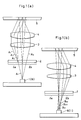
- a laser beam emitted from a light emitting element 11 first passes through a diffracting element 12.
- the diffracted zero-order beam having thus passed through the diffracting element 12 is focused on the recording face of a disk 15 through a collimator lens 13 and an objective lens 14.
- the reflected beam from the recording face of the disk 15 passes through the objective lens 14, the collimator lens 13 and the diffracting element 12.
- the diffracting element 12 is divided into two regions 12a and 12b by a parting line having the same direction as a track on the disk 15, each region having a different diffraction direction.
- the first-order diffracted beam incident on one region 12a of the diffracting element 12 is focused on two divided photo-detecting elements 16a and 16b.
- the diffracted first-order beam incident on the other region 12b is focused on two other photo-detecting elements 16c and 16d.
- the output signals Sa, Sb, Sc and Sd from these photo-detecting elements 16a, 16b, 16c and 16d are then converted into regenerative information signal RF, focusing error signal FE and tracking error signal TE respectively by means of the operational circuit shown in Fig. 11.
- the regenerative information signal RF is detected as a sum of the output signals Sa, Sb, Sc and Sd through adding circuits 20, 21 and 23.
- RF Sa + Sb + Sc + Sd
- the focusing error signal FE is detectable by applying the following operation to the output signals Sa, Sb, Sc and Sd as a sort of the knife edge method.
- FE (Sb + Sc) - (Sa + Sd)
- the tracking error signal TE is detectable by applying the following operation to the output signals Sa, Sb, Sc and Sd as what is called the push-pull method.
- TE (Sc + Sd) - (Sa + Sb) That is, the tracking error TE can be detected by the difference between the intensity of the two light fluxes of laser beam divided by the parting line along the track direction.
- the peak position in the laser beam's intensity distribution is also off the center of the optical axis. This deviation of the peak position off the center of the optical axis influences the difference between the intensity of the two light fluxes of the divided laser beam.
- the present invention relates to an optical pick-up device comprising a light emitting element for producing laser light, an optical system for focusing said laser light onto a recording medium, said optical system including a diffracting element arranged in front of said light emitting element, and photo-detecting means for detecting reflected laser light from said recording medium, a region on said diffracting element being divided into two sub-regions by a parting line substantially perpendicular to a track direction on the recording medium, said diffracting element being arranged such that said reflected light from the recording medium is focused through said optical system onto said photo-detecting means, said device being adapted to detect tracking error signals and focusing error signals from output signals of said photo-detecting means, characterized by one of said sub-regions being adapted to split laser light incident thereon from said light emitting element, thereby forming a main spot and first and second sub-spots on said recording medium for applying the so-called three spot method for detecting focusing and tracking errors.
- This invention has the advantage that manufacturing costs are lower than for known optical pick-up devices since it uses less components and has a simpler construction than known optical pick-up devices. Additionally, if a minor deviation of the optical axis occurs, offset does not take place with regard to the tracking error signal thereby enabling accurate tracking servo control.
- the photo-detecting means comprises two groups of photo-detecting elements each positioned where a respective one of two first-order diffracted beams of the reflected light from said recording medium diffracted by the said other sub-region of said diffracting element are respectively focused.
- a so-called blaze property is imparted to said sub-region of said diffracting element, and there is positioned a group of photo-detecting elements where a first-order beam having higher optical intensity is focused.
- other of said sub-regions comprises a diffraction grating adapted so as to diffract the light reflected toward said photo detecting means in a direction substantially perpendicular to the track direction.
- the photo-detecting means comprises a photo-detecting element for detecting a beam of a main spot reflected from said recording medium said photo-conducting element being divided into two elements by a parting line parallel to said parting line dividing the sub-regions on said diffracting element, the device further comprising an adding circuit for outputting the sum signals output from said respective elements of said photo-detecting element as a regenerative information signal, and a subtracting circuit for outputting a difference signal as a focusing error signal.
- the aforementioned light emitting element and said photo-detecting means are housed in a common package having cap seal window which comprises said diffracting element.
- This embodiment relates to an optical pick-up device of CD player et cetera.
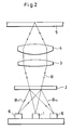
- a light emitting element 1 of an optical pick-up device there are arranged diffracting element 2, collimator lens 3 and objective lens 4 are so arranged that a laser beam A emitted by light emitting element 1 is led to the recording face of a disk 5.
- the aforementioned diffracting element 2 has its region divided into two sub-regions by the parting line approximately perpendicular to the track direction.
- one sub-region 2a there is formed a diffraction grating which causes diffraction approximately in the track direction, as shown in Fig. 1(a).
- Plus one (+1) order and minus one (-1) order diffracted beams of a laser beam A agree with the beams A1 and A2 which form two sub-spots in the 3-spot method.
- the other sub-region 2b of the diffracting element 2 has formed therein another diffraction grating which causes diffraction substantially perpendicular to the track direction, as shown in Fig. 2. That is, the +1 order diffracted beam B11 and the -1 order diffracted beam B12 of the reflected beam B from the disk 5 are divided to both directions perpendicular to the track direction.
- the aforementioned +1 order diffracted beam B11 and -1 order diffracted beam B12 are focused as beams B21, B22 and B23 on the displaced positions in the track direction correspond to the aforementioned two sub-spots and undermentioned main-spot on the recording face of the disk 5.
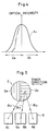
- the beam A3 forming the main-spot in the 3-spot method is formed by the zero-order diffracted beam generated as the laser beam A passes through the sub-regions 2a and 2b of the diffracting element 2. Then, for instance, when the zero-order diffraction efficiency of the diffraction in one sub-region 2a is lower than that in the other sub-region 2b, the optical intensity of the optical line A3 forming the main spot becomes asymmetrical as indicated by the two-dot chain line as shown in Fig. 4, this resulting in deterioration of the regenerative signal et cetera. Hence, both sub-regions 2a and 2b of the diffraction element 2 are set to have the zero-order diffraction efficiencies to be as equal as possible.
- the parting line dividing the aforementioned diffracting element 2 is not an actual line but is an imaginary one cutting off the sub-regions 2a and 2b.
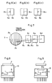
- the light emitting element 1 On the substrate the light emitting element 1 is provided, there are provided two photo-detectors 6, 6 on both sides of the light emitting element 1 in the direction perpendicular to the track direction. These two detectors 6, 6 are located where the +1 order diffracted beam B11 and -1 order diffracted beam B12 of the reflected beam B respectively by the other sub-region 2b are focused. And it is so arranged that the detection sensitivity is increased through synthesis of the output signals from the aforementioned photo-detectors 6, 6.
- the aforementioned photo-detector 6 comprises four photo-detecting elements 6a-6d, each letting out individual outputs.
- Photo-detecting elements 6a, 6b are provided adjacently on both sides of a border line substantially perpendicular to the track direction and the same direction with that of the parting line of diffracting element 2, and the reflected beam B23 of the beam A3 which form a main-spot on the disk 5 is irradiated on this border line.
- the photo-detecting elements 6c, 6d are disposed on both sides of the aforementioned photo-detecting elements 6a, 6b with respect to the track direction and receive the reflected beams B21, B22 of the beams A1, A2, which form sub-spots.
- the aforementioned photo-detecting elements 6a-6b are formed to be sufficiently long in the direction perpendicular to the track direction so as to cope with the variation of the wavelength of the light emitting element 1 and/or displacement of the focal point as a result of assembly errors.
- This signal detection circuit is composed of an adding circuit 7 and two subtracting circuits 8, 9.
- the output signals Sa, Sb are to be added in this adding circuit 7 and then converted into regenerative information signal RF. Also these signals Sa and Sb are subtracted in the subtracting circuit 8 and converted into focusing error signal FE. The aforementioned signals Sc and Sd may also be subtracted in the subtracting circuit 9 and converted into the tracking error signal TE.
- the aforementioned light emitting element 1 and photo-detector 6 are housed into the package 10 in an integrated form. And also a monitoring photo-detector 24 is housed into the package 10 to monitor the light intensity of the light-emitting element 1. Normally such a package 10 has housed therein a light emitting element 1, photo-detector 6 and monitoring photo-detector 24 and is closed with a hermetically sealed glass window 10a, for such elements to be prevented from outside atmosphere such as moisture, oxygen et cetera.
- the diffracting element 2 is disposed before this glass window 10a.
- the diffracting element 2 is directly secured to the package 10 instead of the glass window 10a to seal the interior thereby.
- the number of the necessary parts can be reduced as well as the number of assembly steps.
- the laser beam A emitted from light emitting element 1 first passes through the diffracting element 2.
- the diffracted beam of zero-order having passed both sub-regions 2a, 2b are focused on the recording face of the disk 5 as the beam A3 to form the main-spot.
- the diffracted beams of +1 and -1 order which occur as the laser beam A passes through one sub-region 2a of the diffracted element 2 are focused as beams A1 and A2 in two directions on the recording face of the disk 5 at two positions displaced forward and backward from the main-spot A3 in the approximately track direction and forms two sub-spots.
- the beams B21 - B23 reflected in the individual spots on the recording face of the disk 5 are diffracted as they pass through the other sub-region 2b of the diffracting element 2, and the diffracted beams of +1 and -1 order are focused on the photo-detectors 6, 6.
- the photo-detecting elements 6a, 6b of the individual photo-detectors 6 are irradiated with the reflected beam B23 of the beam A3 which form a main-spot and the signals Sa, Sb are output according to the intensity thereof. These output signals Sa, Sb are added in the adding circuit 7 and are output as the regenerative signal RF.
- the aforementioned reflected beam B23 is a part of the light flux of the reflected beam B which has passed through the other sub-region 2b of the diffracting element 2, that is, what has been diffracted of one side of the light flux divided by the parting line of the diffracting element 2.
- the focal point of the laser beam A is matched as it is focused on the recording face of the disk 5
- the reflected beam B23 is focused as a point on the border line between the photo-detecting elements 6a, 6b as shown in Fig. 6(b).
- a semilunar spot is formed on the photo-detecting element 6a or 6b as the direction of the displacement as shown in Figs. 6 (a)(c).
- focusing error signal FE is output from the subtracting circuit 8 input the output signals Sa, Sb, and it is possible to detect the displacement of the focal point.
- the photo-detecting elements 6c, 6d are irradiated with the reflected beams B21 and B22 of the beams A1 and A2 forming sub-spots, and output signals Sc, Sd are output. And, each intensity of the aforementioned reflected beam B21 and B22 varies in the opposite directions as tracking error according to the 3-spot method.
- the tracking error signal TE is output from the subtracting circuit 9 having received the output signals Sc, Sd.
- the diffracting angle of the reflected beam B diffracted by the diffracting element 2 is caused to be changed, and the focusing position on the photo-detector 6 is thereby displaced in the direction of diffraction.
- the distance between the two sub-spots formed on the recording face of the disk 5 it is desirous to minimize the distance between the two sub-spots formed on the recording face of the disk 5 to prevent the offset of the tracking error signal TE due to the difference in radius of curvature between the tracks on the inner periphery side and the outer periphery side.
- the aforementioned distance between the sub-spots is desirous to be minimized also for preventing the deterioration of the detecting precision of the tracking error signal TE due to the positioning error as the pick up device is attached to a CD player or the like.
- the photo-detecting elements 6c, 6d it is essential that these be disposed on both sides along the track direction of the photo-detecting element 6a, 6b. Hence it is preferable to set the distance between the aforementioned photo-detecting elements 6c and 6d as small as possible.
- the diffraction angle of the reflected beam B diffracted by the diffracting element 2 varies according to the variation of the oscillation wavelength of the light emitting element 1.
- the sub-spot formed on the recording face of the disk 5 is preferably formed approximately oval with its long axis parallel to the track direction.
- One sub-region 2a of the diffracting element 2 in which the beams A1, A2 forming sub-spots are apart from the laser beam A is desirous to be small in dimension and less in the number of diffraction gratings in the track direction.
- the sub-regions 2a, 2b are divided in two by a parting line crossing the track direction approximately at right angle and thereby it is possible to detect tracking error signal TE et cetera not including offsets, regardless of the variation in wavelength, and moreover lowering of the manufacturing cost can be attained by increasing the allowable range for the position at which the optical pick-up device is attached.
- An optical pick-up device of such a composition enables detecting the focusing error signal by a sort of knife edge method similar to the prior art cited, and also the tracking error signal can be detected by the 3-spot method which is known to be highly reliable for the tracking error signal, hence there is no problem of offset being caused with regard to the tracking error signal due to displacement of optical axis in the optical system.
Applications Claiming Priority (2)
| Application Number | Priority Date | Filing Date | Title |
|---|---|---|---|
| JP97496/88 | 1988-04-20 | ||
| JP63097496A JPH0770065B2 (ja) | 1988-04-20 | 1988-04-20 | 光ピックアップ装置 |
Publications (3)
| Publication Number | Publication Date |
|---|---|
| EP0338840A2 EP0338840A2 (en) | 1989-10-25 |
| EP0338840A3 EP0338840A3 (en) | 1990-07-04 |
| EP0338840B1 true EP0338840B1 (en) | 1993-12-29 |
Family
ID=14193874
Family Applications (1)
| Application Number | Title | Priority Date | Filing Date |
|---|---|---|---|
| EP89303962A Expired - Lifetime EP0338840B1 (en) | 1988-04-20 | 1989-04-20 | Optical pick-up device |
Country Status (6)
| Country | Link |
|---|---|
| US (1) | US5111449A (ja) |
| EP (1) | EP0338840B1 (ja) |
| JP (1) | JPH0770065B2 (ja) |
| KR (1) | KR920005263B1 (ja) |
| CA (1) | CA1329262C (ja) |
| DE (1) | DE68911730T2 (ja) |
Families Citing this family (35)
| Publication number | Priority date | Publication date | Assignee | Title |
|---|---|---|---|---|
| US4983017A (en) * | 1988-08-02 | 1991-01-08 | Sharp Kabushiki Kaisha | Optical head device for reading information stored in a recording medium |
| JPH083910B2 (ja) * | 1989-01-13 | 1996-01-17 | シャープ株式会社 | 光ピックアップ装置 |
| JPH087872B2 (ja) * | 1990-01-19 | 1996-01-29 | 松下電器産業株式会社 | 光ヘッド装置 |
| JP2655923B2 (ja) * | 1990-01-22 | 1997-09-24 | シャープ株式会社 | 光ヘッド装置 |
| JP2711010B2 (ja) * | 1990-04-04 | 1998-02-10 | 株式会社日本コンラックス | 光学ヘッド |
| DE69128808T2 (de) * | 1990-04-12 | 1998-07-23 | Matsushita Electric Ind Co Ltd | Optischer Kopf mit hologrammverbundener Objektivlinse |
| US5202869A (en) * | 1990-04-20 | 1993-04-13 | Sharp Kabushiki Kaisha | Optical head device including diffraction grating |
| JPH0721869B2 (ja) * | 1990-04-20 | 1995-03-08 | シャープ株式会社 | 光ピックアップ装置 |
| JP2656136B2 (ja) * | 1990-05-29 | 1997-09-24 | シャープ株式会社 | 光ピックアップ装置 |
| JP3028854B2 (ja) * | 1990-07-18 | 2000-04-04 | セイコーエプソン株式会社 | 光ヘッド及び光記憶再生装置 |
| JP2776487B2 (ja) * | 1992-01-28 | 1998-07-16 | シャープ株式会社 | 光学式情報記録再生装置 |
| US5446719A (en) * | 1992-02-05 | 1995-08-29 | Sharp Kabushiki Kaisha | Optical information reproducing apparatus |
| EP0579843B1 (en) * | 1992-02-07 | 1999-12-22 | Sony Corporation | Optical pickup apparatus for magneto-optical storage |
| DE69319673T2 (de) * | 1992-08-12 | 1999-02-25 | Philips Electronics Nv | Einrichtung zur optischen Abtastung einer Oberfläche |
| KR940020325A (ko) * | 1993-02-08 | 1994-09-15 | 이헌조 | 광픽업장치 |
| US5517479A (en) * | 1993-03-26 | 1996-05-14 | Matsushita Electronics Corporation | Optical head including a semiconductor laser having a non-scatter incident area |
| JPH07114746A (ja) * | 1993-08-25 | 1995-05-02 | Sony Corp | 光学装置 |
| JP3541416B2 (ja) * | 1994-03-08 | 2004-07-14 | ソニー株式会社 | 光学装置 |
| JPH09265639A (ja) * | 1996-01-23 | 1997-10-07 | Sony Corp | 光学ピックアップ装置 |
| US5652744A (en) * | 1996-02-08 | 1997-07-29 | Industrial Technology Research Institute | Single surface diffractive element for optical pickup heads |
| US6556533B1 (en) * | 1996-10-01 | 2003-04-29 | Matsushita Electric Industrial Co., Ltd. | Optical pickup device |
| EP0990187B1 (en) * | 1998-04-17 | 2005-07-20 | Koninklijke Philips Electronics N.V. | Method of manufacturing a lens system comprising two lens elements |
| CN1155957C (zh) * | 1998-06-30 | 2004-06-30 | 株式会社三协精机制作所 | 光传感装置 |
| EP0990927A3 (en) | 1998-09-28 | 2000-12-13 | Sharp Kabushiki Kaisha | Diffraction grating having multiple gratings with different cycles for generating multiple beams and optical pickup using such diffraction grating |
| JP3545233B2 (ja) * | 1998-12-08 | 2004-07-21 | シャープ株式会社 | 球面収差検出装置および光ピックアップ装置 |
| JP2001014717A (ja) * | 1999-04-28 | 2001-01-19 | Matsushita Electronics Industry Corp | 光学装置 |
| US20050068864A1 (en) * | 1999-07-08 | 2005-03-31 | Samsung Electronics Co., Ltd. | Method and apparatus for tracking error detection in optical disk driver |
| TW501116B (en) * | 2000-07-05 | 2002-09-01 | Matsushita Electric Ind Co Ltd | Optical device, optical semiconductor device, and optical information processor comprising them |
| JP2002250809A (ja) * | 2001-02-26 | 2002-09-06 | Alps Electric Co Ltd | 光学部材およびそれを用いた光ピックアップ |
| KR100452293B1 (ko) * | 2002-01-07 | 2004-10-08 | 삼성전기주식회사 | 광 픽업장치 |
| JP3977234B2 (ja) * | 2002-04-24 | 2007-09-19 | シャープ株式会社 | 光ピックアップ |
| KR100480786B1 (ko) * | 2002-09-02 | 2005-04-07 | 삼성전자주식회사 | 커플러를 가지는 집적형 광 헤드 |
| US7209427B2 (en) * | 2003-06-19 | 2007-04-24 | Matsushita Electric Industrial Co., Ltd. | Optical pickup with reduced size |
| JP2006059416A (ja) * | 2004-08-18 | 2006-03-02 | Sony Corp | 光ディスク装置およびその制御方法 |
| US20090206104A1 (en) * | 2006-07-18 | 2009-08-20 | Loranger Linda S | Dispensing system for dispensing individual portions of a food product from a food product container |
Family Cites Families (15)
| Publication number | Priority date | Publication date | Assignee | Title |
|---|---|---|---|---|
| NL8502835A (nl) * | 1985-10-17 | 1987-05-18 | Philips Nv | Inrichting voor het met optische straling aftasten van een informatievlak. |
| EP0222238B2 (en) * | 1985-11-11 | 1998-02-11 | Sharp Kabushiki Kaisha | Pick-up device |
| JPS6356819A (ja) * | 1986-08-27 | 1988-03-11 | Nec Corp | 光ヘツド装置 |
| EP0228620B1 (en) * | 1985-12-10 | 1991-06-05 | Nec Corporation | Optical head comprising a diffraction grating for directing two or more diffracted beams to optical detectors |
| KR950005031B1 (ko) * | 1986-02-24 | 1995-05-17 | 소니 가부시끼가이샤 | 초점 검출 장치 |
| JP2515504B2 (ja) * | 1986-08-05 | 1996-07-10 | 三菱電機株式会社 | 光学式ヘツド装置 |
| EP0241942B1 (en) * | 1986-04-18 | 1992-03-04 | Mitsubishi Denki Kabushiki Kaisha | Optical type head device |
| JPS62251963A (ja) * | 1986-04-25 | 1987-11-02 | Casio Comput Co Ltd | Icカ−ドの認証方式 |
| US4794585A (en) * | 1986-05-06 | 1988-12-27 | Lee Wai Hon | Optical head having a hologram lens and polarizers for use with magneto-optic medium |
| KR900008380B1 (ko) * | 1986-07-01 | 1990-11-17 | 미쓰비시덴기 가부시기 가이샤 | 광학식 헤드장치 |
| NL8601974A (nl) * | 1986-08-01 | 1988-03-01 | Philips Nv | Inrichting voor het met optische straling aftasten van een stralingsreflekterend informatievlak. |
| JPS63285732A (ja) * | 1987-05-19 | 1988-11-22 | Pioneer Electronic Corp | 光学式ピックアップ装置 |
| NL8702245A (nl) * | 1987-09-21 | 1989-04-17 | Philips Nv | Inrichting voor het met optische straling aftasten van een stralingsreflekterend informatievlak. |
| JP2800156B2 (ja) * | 1987-10-06 | 1998-09-21 | 三菱電機株式会社 | 光学式ヘッド装置 |
| JPH01151022A (ja) * | 1987-12-09 | 1989-06-13 | Sharp Corp | 光ピックアップ装置 |
-
1988
- 1988-04-20 JP JP63097496A patent/JPH0770065B2/ja not_active Expired - Fee Related
-
1989
- 1989-04-19 CA CA000597187A patent/CA1329262C/en not_active Expired - Lifetime
- 1989-04-20 DE DE68911730T patent/DE68911730T2/de not_active Expired - Lifetime
- 1989-04-20 EP EP89303962A patent/EP0338840B1/en not_active Expired - Lifetime
- 1989-04-20 KR KR1019890005211A patent/KR920005263B1/ko not_active IP Right Cessation
-
1990
- 1990-05-11 US US07/522,631 patent/US5111449A/en not_active Expired - Lifetime
Also Published As
| Publication number | Publication date |
|---|---|
| KR920005263B1 (ko) | 1992-06-29 |
| DE68911730T2 (de) | 1994-07-21 |
| KR890016525A (ko) | 1989-11-29 |
| EP0338840A3 (en) | 1990-07-04 |
| JPH0770065B2 (ja) | 1995-07-31 |
| DE68911730D1 (de) | 1994-02-10 |
| JPH01269239A (ja) | 1989-10-26 |
| CA1329262C (en) | 1994-05-03 |
| EP0338840A2 (en) | 1989-10-25 |
| US5111449A (en) | 1992-05-05 |
Similar Documents
| Publication | Publication Date | Title |
|---|---|---|
| EP0338840B1 (en) | Optical pick-up device | |
| EP0378438B1 (en) | An optical pickup apparatus | |
| US5065380A (en) | Diffraction grating for an optical pickup device | |
| US4907847A (en) | Optical pickup and hologram therefor | |
| EP0075676B1 (en) | Optical track position detecting apparatus and optical disc apparatus using the same | |
| JPH07129980A (ja) | 光ピックアップ | |
| US6104689A (en) | Sensor system for optical disc drive | |
| EP0951716B1 (en) | Optical scanning device | |
| EP0612064B1 (en) | An optical pickup apparatus | |
| US5018804A (en) | Laser pick-up | |
| US7064900B2 (en) | Optical pickup device and optical disk device and optical device and composite optical element | |
| EP0311463A2 (en) | An optical information reproducing apparatus | |
| US6512732B1 (en) | Device for optically scanning information tracks on a plane using two subbeams | |
| US6614743B1 (en) | Semiconductor laser device | |
| EP0605929B1 (en) | Device for optically scanning a surface | |
| KR20040090967A (ko) | 광 픽업 | |
| JP2596812B2 (ja) | 光ピックアップにおける再生信号検出方法 | |
| JP3530383B2 (ja) | 光ピックアップ装置 | |
| JP2623796B2 (ja) | 光ヘッド装置及びその組立方法 | |
| JPH02193333A (ja) | 光ピックアップ | |
| KR200172921Y1 (ko) | 홀로그램소자를 채용한 광픽업 장치 | |
| JP2005116089A (ja) | 回折素子およびそれを用いた半導体レーザ装置、光ピックアップ装置 | |
| JPH052762A (ja) | 光学式記録再生装置 | |
| JPH0258739A (ja) | 光ヘッド装置 | |
| JPH0242648A (ja) | 光学式情報読取装置 |
Legal Events
| Date | Code | Title | Description |
|---|---|---|---|
| PUAI | Public reference made under article 153(3) epc to a published international application that has entered the european phase |
Free format text: ORIGINAL CODE: 0009012 |
|
| 17P | Request for examination filed |
Effective date: 19890512 |
|
| AK | Designated contracting states |
Kind code of ref document: A2 Designated state(s): DE FR GB NL |
|
| PUAL | Search report despatched |
Free format text: ORIGINAL CODE: 0009013 |
|
| AK | Designated contracting states |
Kind code of ref document: A3 Designated state(s): DE FR GB NL |
|
| 17Q | First examination report despatched |
Effective date: 19920227 |
|
| GRAA | (expected) grant |
Free format text: ORIGINAL CODE: 0009210 |
|
| AK | Designated contracting states |
Kind code of ref document: B1 Designated state(s): DE FR GB NL |
|
| REF | Corresponds to: |
Ref document number: 68911730 Country of ref document: DE Date of ref document: 19940210 |
|
| ET | Fr: translation filed | ||
| PLBE | No opposition filed within time limit |
Free format text: ORIGINAL CODE: 0009261 |
|
| STAA | Information on the status of an ep patent application or granted ep patent |
Free format text: STATUS: NO OPPOSITION FILED WITHIN TIME LIMIT |
|
| 26N | No opposition filed | ||
| REG | Reference to a national code |
Ref country code: GB Ref legal event code: IF02 |
|
| PGFP | Annual fee paid to national office [announced via postgrant information from national office to epo] |
Ref country code: DE Payment date: 20080424 Year of fee payment: 20 Ref country code: FR Payment date: 20080312 Year of fee payment: 20 |
|
| PGFP | Annual fee paid to national office [announced via postgrant information from national office to epo] |
Ref country code: NL Payment date: 20080415 Year of fee payment: 20 |
|
| PGFP | Annual fee paid to national office [announced via postgrant information from national office to epo] |
Ref country code: GB Payment date: 20080423 Year of fee payment: 20 |
|
| REG | Reference to a national code |
Ref country code: GB Ref legal event code: PE20 Expiry date: 20090419 |
|
| PG25 | Lapsed in a contracting state [announced via postgrant information from national office to epo] |
Ref country code: NL Free format text: LAPSE BECAUSE OF EXPIRATION OF PROTECTION Effective date: 20090420 |
|
| NLV7 | Nl: ceased due to reaching the maximum lifetime of a patent |
Effective date: 20090420 |
|
| PG25 | Lapsed in a contracting state [announced via postgrant information from national office to epo] |
Ref country code: GB Free format text: LAPSE BECAUSE OF EXPIRATION OF PROTECTION Effective date: 20090419 |