EP0338655A2 - Analog-Digitalwandler mit Kompensation des integralen Linearitätsfehler - Google Patents
Analog-Digitalwandler mit Kompensation des integralen Linearitätsfehler Download PDFInfo
- Publication number
- EP0338655A2 EP0338655A2 EP89300745A EP89300745A EP0338655A2 EP 0338655 A2 EP0338655 A2 EP 0338655A2 EP 89300745 A EP89300745 A EP 89300745A EP 89300745 A EP89300745 A EP 89300745A EP 0338655 A2 EP0338655 A2 EP 0338655A2
- Authority
- EP
- European Patent Office
- Prior art keywords
- analog
- voltage
- error
- divider
- comparators
- Prior art date
- Legal status (The legal status is an assumption and is not a legal conclusion. Google has not performed a legal analysis and makes no representation as to the accuracy of the status listed.)
- Granted
Links
Images


Classifications
-
- H—ELECTRICITY
- H03—ELECTRONIC CIRCUITRY
- H03M—CODING; DECODING; CODE CONVERSION IN GENERAL
- H03M1/00—Analogue/digital conversion; Digital/analogue conversion
- H03M1/06—Continuously compensating for, or preventing, undesired influence of physical parameters
- H03M1/0602—Continuously compensating for, or preventing, undesired influence of physical parameters of deviations from the desired transfer characteristic
- H03M1/0612—Continuously compensating for, or preventing, undesired influence of physical parameters of deviations from the desired transfer characteristic over the full range of the converter, e.g. for correcting differential non-linearity
-
- H—ELECTRICITY
- H03—ELECTRONIC CIRCUITRY
- H03M—CODING; DECODING; CODE CONVERSION IN GENERAL
- H03M1/00—Analogue/digital conversion; Digital/analogue conversion
- H03M1/12—Analogue/digital converters
- H03M1/34—Analogue value compared with reference values
- H03M1/36—Analogue value compared with reference values simultaneously only, i.e. parallel type
- H03M1/361—Analogue value compared with reference values simultaneously only, i.e. parallel type having a separate comparator and reference value for each quantisation level, i.e. full flash converter type
- H03M1/362—Analogue value compared with reference values simultaneously only, i.e. parallel type having a separate comparator and reference value for each quantisation level, i.e. full flash converter type the reference values being generated by a resistive voltage divider
- H03M1/365—Analogue value compared with reference values simultaneously only, i.e. parallel type having a separate comparator and reference value for each quantisation level, i.e. full flash converter type the reference values being generated by a resistive voltage divider the voltage divider being a single resistor string
Definitions
- This invention relates to analog to digital converters, and it relates in particular to circuits for compensating for integral linearity error in the output of such converters.
- each input analog signal sample is simultaneously compared to a plurality of different reference signal levels to determine approximately what the sample amplitude is.
- One comparator of a type commonly used in the art is disclosed in U.S.A. Patent No. 3,676,702 to E. P. McGrogan, Jr., the disclosure of which is hereby incorporated herein by reference.
- the determined amplitude value is then converted to a corresponding digitally represented, e.g., binary coded, value for such further utilization as may be appropriate.
- the analog to digital converter includes means for developing a plurality of different reference voltages, means for comparing an input analog signal to said plurality of different reference voltages to develop a digital output signal corresponding to said analog input signal, said output signal including a predetermined degree of integral linearity error, and means coupled to said developing means for generating a further error in a sense to offset at least in part said integral linearity error.
- the further error is generated by reducing the resistance of a central portion of a reference supply voltage divider for sampling comparators in the analog to digital converter at each recurrent time of application of reference voltage to the comparators.
- a fixed duration time intervai is established for applying the resistance reduction so that the amount of the resistance reduction need not be changed when the sampling frequency of the converter is changed.
- FIG. 1 illustrates an analog to digital converter 10 within the outer dashed-line box utilizing integral linearity error compensation of the present invention.
- Each comparator is advantageously of the type described in the aforementioned McGrogan patent and, for the convenience of the reader, further illustrated and described herein in connection with FIG. 7.
- Comparators of the set 13 are individually referenced to different voltage levels provided by a compensated reference voltage supply 17 shown within a dashed box in FIG. 1. Compensation is provided in accordance with one aspect of the invention to offset at least in part the effect of integral linearity error in converter 10 output and believed to be the result of parasitic capacitance in comparators 12.
- the compensation is illustratively implemented, as will be subsequently further described, by recurrent connection of at least one resistance shunt, e.g. R28 and R33, to alter the voltage distribution among output reference terminals of supply 17 during times when the parasitic effects are most damaging to linearity.
- Recurrent connection is achieved by clocked logic including a gate 29, inverters 30 and 32, and transistors 31 and 36.
- Output states of 256 comparators 12 are captured in respective latch circuits 18 and decoded to an N-bit digital output signal by a decode and parallel logic array circuit 19.
- the compensated reference supply 17 and comparators 12 of FIG. 1 will now be considered in greater detail in connection with the FIGS. 4 and 5 timing diagrams of comparator input analog and reference sampiing functions, respectively, the FIG. 6 reference compensation switching function, the FIG. 7 simplified circuit diagram of an illustrative one of comparators 12, and the signal versus time diagrams of FIGS. 8-11 illustrating comparator operation.
- each comparator simultaneously samples alternately, under control of complementary clock signals CL1 and CL1′ from a clock signal supply 16, its signal monitoring input and a reference voltage input from the compensated reference voltage supply 17. That strobing of the comparator input terminals may be at any of predetermined rates, and it is here illustratively considered to be in the range of 10 MHz to 20 MHZ.
- Parasitic capacitance associated with the sampling function of each comparator 12 is schematically represented by respective parasitic capacitors Cp connected to the comparators.
- a supply voltage resistance of approximately 500 ohms is illustratively employed for a converter intended to operate in a sampling frequency range of ten to twenty megahertz (MHz) using comparators implemented in metal oxide semiconductor (MOS) technology.
- MOS metal oxide semiconductor
- comparator parasitic capacitances are unable to adjust their charges to stable conditions sufficiently rapidly at those frequencies, and the aforementioned integral linearity error results, as will be further discussed in connection with FIG. 2. That error is largely offset, in accordance with the present invention, by recurrently modifying the reference supply during a beginning portion, e.g., around a time t2 in FIG. 5, of each sampling interval portion when comparators are sampling the reference voltage. The modification generates an at-least-partially offsetting reference voltage error as will be further described subsequently.
- Comparators 12 each operates so that its output is a low, or binary ZERO, signal if the voltage V IN at its signal monitoring input is less than a predetermined, threshold, voltage level determined by the voltage V r , indicated in FIG. 7, connected to its reference input; and its output is a high, or binary ONE, signal if the voltage at its signal monitoring input is more than the threshold voltage level. Consequently, comparators 12 connected to output taps from reference supply 17 which are at voltages less than a present input analog signal sample exhibit a high, binary ONE, output; and comparators 12 connected to reference output taps at voltages greater than a present input analog signal sample exhibit a low, binary ZERO, output.
- Such an output signal array is in the art sometimes called a "thermometer scale” or a “bar coded scale;” and it is hereinafter called a bar coded scale.
- Outputs from the comparator set 13 are coupled through clocked latches 18, such as the well known D-type bistable circuits, to inputs of a decode-and-parallel-logic-array circuit 19.
- Circuit 19 includes logic circuits, of the type indicated in the aforementioned Dingwall paper, for performing two functions.
- the clock signal supply16 fixes the converter sampling rate by providing the aforementioned complementary clocking signals to the comparators 12.
- Supply 16 also provides a sample rate signal CL5 to latches 18 to enable them to sample comparator outputs after they have settled following sampling of V IN .
- the CL6 output of supply 16 enables circuit 19 to receive and process the latch outputs after new latch states have settled.
- a clock supply output CL14 is provided to reference supply 17 just prior to the time for sampling of reference outputs by the comparators to enable the recurrent compensation function in reference supply 17.
- Reference supply 17 includes a resistive voltage divider 22 (shown within a dashed-line rectangle) which is divided into a plurality of equal resistances R, one of which is split into two halves, each half R/2 being connected at a different end of the overall divider.
- Each resistor R is approximately two ohms in the illustrative 256-comparator embodiment. Only eight of the divider resistances are actually shown. Tap circuits are connected to series circuit junction points between adjacent ones of the resistors of divider 22 and extend to the respective reference input terminals of the comparators of the set 13.
- the comparators are connected to regularly, i.e., equally, spaced resistance points on divider 22 and, in an ideal case, i.e., absent integral linearity error, they would be referenced to correspondingly equally spaced voltage points on the divider.
- the series combination of resistances R is connected across a voltage supply V REF , otherwise designated 21 and schematically represented as a circled polarity sign to indicate connection to a source terminal of that polarity with the opposite polarity terminalconnected to ground.
- a capacitor 25 bypasses midscale tap circuit 24 to ground for noise, e.g., at the sampling rate, to stabilize the converter.
- capacitance of capacitor 25 is 0.1 microfarad.
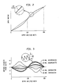
- FIG. 2 illustrates by a solid line the ideal converter input voltage versus output voltages.
- the output voltage is in terms of 256 LSB-sized divisions, here called amplitude units, of the iilustrative 5-volt output voltage range.
- Operation of the converter 10 as described so far is well known to produce integral linearity error in that characteristic in high speed operations such as in the 10 to 20 MHz range of sampling frequencies.
- the real characteristic includes error in the ideal linearity of reference voltage distribution along the divider 22 as illustrated by the dashed curve in FIG. 2.
- the dashed curve is actually made up of a stepped waveform corresponding to the LSB-sized steps in the digital approximation of converter input analog values.
- FIG. 3 shows the same information replotted on the basis of integral linearity error versus output amplitude units.
- the stepwise digital approximation becomes a sawtooth of about one LSB amplitude superimposed on a curve having a shape similar to that of the real characteristic in FIG. 2.
- Two such composite curves are shown in FIG. 3. a relatively small one for a 10MHz sampling rate embodiment and a larger one for a 20 MHz embodiment.
- Corresponding dashed-line curves for compensating generated error, to be subsequently described, are also shown in FIG. 3. It is believed that the error is due to parasitic capacitance effects in the respective comparators, as described in the aforementioned Dingwall paper.
- the real error characteristic exhibits zero error with respect to the ideal at the zero, near midscale 128, and at full scale 256 output amplitudes regardless of sampling rate.
- Each generated error characteristic is approximately a mirror image of the corresponding real error characteristic, but the generated error exhibits more accentuated peaks than does the real error.
- FIGS. 4 and 5 are timing diagrams showing the complementary clock signals CL1 and CL1′ employed to strobe comparators 12. It is observed that those clock signals are asymmetrical in that ON, or high signal, times are different from 0FF, or low signal times. Use of such asymmetry and its advantages are considered at length in a U.S.A. Patent No. 4,633,222 to A. G. F. Dingwall and entitled "Clock Shaping Circuit and Method.”
- FIG. 7 shows a simpiified diagram of an arbitrary one of the comparators 12 with an analog signal input terminal 37, to which the input signal VIN (from converter 10 input terminals 11 in FIG. 1) is applied in parallel to all of comparators 12.
- a comparator reference input terminal 38 receives a reference voltage Vr, from a tap between adjacent arbitrary ones of resistors R of divider 22 of reference supply 17 in FIG. 1.
- Reference voltage Vr has a different value for each comparator 12.
- Terminals 37 and 38 are alternately coupled to a common signal input terminal 39 and a capacitor 40 through switches 41 and 42, respectively, under control of the clock signals of FIGS. 4 and 5.
- Capacitor 40 couples the voltage variations at terminal 39 to an input terminal 43 of an auto-zeroed inverter 46 which has a feedback circuit switched in conjunction with the switching of the reference input, i.e., the output and input of inverter 46 are connected together by a switch 44 while the comparator reference input 38 is being sampled between times t2 and t4 and after time t6 of FIGS. 4-6 and 9-10.
- Parasitic capacitances C Pa and C Pb schematically shown connected adjacent to terminals 39 and 43, respectively, will be further discussed subsequently.
- a latch circuit 18 registers the output of inverter 45 for appropriate utilization.
- switches 41, 42, and 44 are implemented in complementary Metal-Oxide- Semiconductor (MOS) technology and exhibit resistances of about five kilohms in the present state of the art.
- MOS Metal-Oxide- Semiconductor
- FIGS. 8-11 are voltage versus time diagrams illustrating the operation of the comparator of FIG. 7 in a low frequency case where parasitic capacitances do not interfere with converter linearity.
- the illustration assumes an example in which the voltage of the reference source 21 in FIG. 1 is 5 volts, the comparator reference input terminal 38 (of FIG. 7) is connected at a 3-volt tap on divider 22, and the analog input voltage V IN is initially zero volts and changes to 4 volts just before time t4 as shown in FIG. 8. Initially, prior to time t0, switches 42 and 44 are ON (closed) and switch 41 is 0FF (open).
- Terminal 39 (V39) is at the V r voltage of 3 volts; and, because of the feedback through switch 44, terminals 43 (V43) and 48(V48) are autozeroed at one-half the supply voltage. That supply voltage is included in the schematic representation of inverter 46.
- switch 41 is turned ON to sample input voltage V IN , and switches 42 and 44 are turned OFF. Voltages at terminals 39 and 43 shift down by somewhat less than 3 volts, due to charge division between capacitor 40 and parasitic capacitance C Pb thereby causing the voltage V48 at the output of inverter 46 to switch to nearly 5 volts.
- the latch 18 Prior to time t2, the latch 18 is enabled to register the inverter output voltage level at terminal 48.
- switch states change to sample the reference voltage V r again.
- the analog input changes to 4 volts as shown in FIG. 8.
- switch 41 is turned 0FF, and switches 42 and 44 are turned ON, and the terminal voltages begin adjusting to the new analog voltage value as shown in FIGS. 9-11.
- Each comparator is referenced at the same time to its particular voltage V r from divider 22.
- Parasitic capacitances delay the immediate achievement of the ideal reference charge, the difference between V43 and V39, on capacitor 40.
- the time required for that achievement depends upon the size of the least prior sample voltage V IN to all comparators and the size of the voltage V r to which a particular comparator must adjust. In applications such as that of the illustrative embodiment where sampling rate may be in the range of 10 MHz to 20 MHz, there is insufficient time to allow full stabilization of the parasitics of all of the comparators. The consequence of incomplete stabilization is improper referencing, and error in converter output results as already mentioned.
- each comparator parasitic As each comparator parasitic adjusts its charge state toward its particular reference voltage V r , it charges or discharges depending upon whether its voltage V39 is greater than or less than its tap voltage V r .
- One comparator which is referenced to a tap voltage which is at least approximately equal to the last prior input analog voltage V IN is here for convenience called a reference comparator, and its parasitic capacitance experiences little or no charging change during a reference sampling interval when that equality exists.
- the charging or discharging current flows through a portion of divider 22 and returns through parasitics of one or more other comparators which are discharging or charging, respectively. It can be said that the parasitic capacitances of such other comparators, above and below the reference comparator along the reference voltage divider, exchange charges.
- the currents injected into, or extracted from, parts of divider 22 during such an exchange alter the IR drop distribution, i.e., change the effective tap electrical spacing, among the divider resistances from the ideal distribution which would have yielded linear converter operation.
- the effective electrical spacing of the divider taps is dynamically changed; so that, for the short interval when the reference is first appiied, the taps in a central region are more widely spaced electrically than are the taps in regions on either end of the divider outside the centrai region.
- the divider taps near the ends of divider 22 have zero or low error because they are essentially clamped at the reference voltage terminals or are subjected to relatively little parasitic capacitor current component flow.
- the midscale tap region has zero error because parasitic currents in the top half of the divider tend to make the V r of the tap at midscale lower than ideal, and those in the lower half tend to make V r at midscale higher than ideal. So the two effects tend to balance out to about zero on average near the midscale point.
- V r error components of opposite senses with respect to those due to parasitic capacitances.
- unusually low switch resistances would be less than one kilohm.
- the generated error components indicated by dashed lines in FIGS. 2 and 3, are made to be of sufficient magnitude to reduce the net error, i.e., uncompensated error minus generated error, to a tolerable level for a particular type of application of the converter 10.
- the further error components also transiently modify the effective spacing of divider taps, but in this case the modification has the effect of reducing tap spacing in the central region of the divider and increasing tap spacing in the end regions. That effect tends to cancel the previously mentioned wider spacing without compensation.
- the error generating means comprises circuits for shunting a central part of the divider 22 resistance during a beginning portion of the reference sampling phase of the converter operating cycle as illustrated in FIG. 6.
- the shunt is connected between times t1 and t3 and times t5 and t7.
- the resistance of the shunt and the location of its connections are selected to increase the IR drop in unshunted end regions of the divider 22, thereby accelerating the parasitic recovery and tending to restore the normal IR drop distribution among divider parts more quickly.
- the amount of the shunt resistance is that which approximately equalizes amplitudes of uncompensated error and error after compensation.
- Compensation for integral linearity error is achieved illustratively by shunting at least one central portion of the resistances R by a resistance approximately an order of magnitude larger than the divider 22 resistance during at least a beginning portion of a sampling interval part when the comparators 12 are sampling their respective reference voltages from supply 17.
- a resistor 28 is connected in series with the source-drain path of an N-channel MOS transistor switch 31 between symmetrically located circuit points on divider 22. Those points are advantageously slightly inside the one-quarter and three-quarter scale taps on the divider, i.e., slightly closer than those taps are to the midscale tap 24.
- the uncompensated error curve has maximum amplitudes in regions of the curve which are relatively flat.
- a position is typically selected by trial, and error to produce the lowest error amplitude, and that usually occurs when the positive and negative lobes of the compensated error curve are approximately equal.
- Such a curve is the dashed curve of FIG. 12. That curve includes in each half of the error characteristic a narrow central overcompensation lobe, of polarity opposite to the polarity of the lobe of the same half of the uncompensated characteristic, fianked by two broad lobes of the same polarity as that uncompensated lobe. As indicated in FIG. 12, the overcompensation lobes occur at approximately the quarter points indicated by output ampiitude counts of 64 and 192.
- the leading edge of the clock signal CL14 in FIG. 6 is coupled through a NAND gate 29 and an inverter 30 to the gate terminal of transistor 31 to turn that transistor ON for conduction in the shunt including resistor 28. (If an additional shunt including a resistor 33 is provided, as will be subsequently discussed, its transistor 36 is also turned ON at the same time.)
- the same clock pulse leading edge is coupled through a series of an odd number of tandem connected inverters 32, gate 29, and inverter 30 to turn the transistor 31 0FF a fixed time later. That fixed time is the same, regardless of the clock frequency; and in the illustrative embodiment, it is made to be about 25 nanoseconds by employing 21 inverters in the series 32.
- Inverters 30 and 32 are advantageously the type shown in the McGrogan patent, each inverter using a pair of complementary conductivity type MOS transistors. Use and advantages of a logic combination such as that of gate 29 and inverters 30 and 32 as a fixed pulse width generator is disclosed in the aforementioned Dingwall patent.
- the CL 14 clock signal actuates transistor 31; and it goes high at times t1 and t5, somewhat before gates 42 and 44 are actuated together, at leading-edge times t2 and t6,to sample the reference voltage.
- the time lead ahead of the leading edge time of the reference sampling function allows time for the shunt switching transients to settle before the sampling begins.
- the relatively long interval between times t1 and t3 allows the maximum opportunity for parasitic capacitance charges to stabilize at proper charge levels for representing respective reference voltages. That interval is fixed independently of clock frequency by virtue of the nature of the clock coupling circuit for clocking transistor 31. Consequently, if clock frequency is changed, the switching frequency of the shunt connecting transistor changes; and the duty cycle of the clock wave CL14 changes in the same sense; but the width of the switch turn-on pulse between times t1 and t3 stays the same.
- the clock frequency i.e., the converter input sampling rate
- the clock frequency can be set at different values without the need to redetermine an appropriate new resistance for the reference divider shunt to match the reduced or elongated reference sampling time resulting from the frequency change.
- the transient error correction effects die out, and the final divider correction is negligible.
- transient effects of error compensation contribute corrections which increase in proportion with sampling rate. Increasing correction results until the reference pulse becomes slightly shorter than the correction pulse, the maximal correction point.
- the effect of the reference divider shunt is to reduce the total parallel resistance of the shunted portion of the reference divider. Hence, the voltage drop across the shunted portion of the divider is reduced, and the voltage drops across the remaining divider portions at either end of the reference divider are increased. This redistribution of divider voltages causes corresponding changes in the voltages at the respective tap circuits, and those changes have been found to comprise a further error which largely offsets the aforementioned integral linearity error.
- FIG. 12 illustrates integrated linearity error for several different situations.
- Shunt resistor 28 is also indicated adjacent to the curves of FIG. 12 to illustrate the relationships of the shunt connection points to various features of the curves.
- a solid-line curve indicates in simplified form the uncorrected error for the 20 MHz case, which was illustrated in FIG. 3 with superimposed sawtooth variations.
- Dashed curves in FIG. 12 illustrate the error reduction improvement resulting from the single-shunt compensation for reference divider 22. It has been found in practice, and as shown in FIG. 12, that a single shunt results in a moderate amount of overcompensation, i.e., about one LSB of positive error at the uncorrected negative maximum and one LSB of negative error at the uncorrected positive maximum.
- This second shunt includes a resistor 33 and another N-channel MOS transistor 36 connected in series between output count locations outside of the overcompensated maxima for the single-shunt case, i.e., between about the symmetrical 58-count and 198-count points in the illustrative embodiment. Those points are also outside of the one-quarter and three-quarter scale points of the divider 22 and define the outer limits of the central portion of the illustrative divider 22 Which is shunted for integral linearity error compensation.
- Resistor 33 is illustrativeiy of approximately 5500 ohms for the 10 MHz to 20 MHz example considered here in which the innermost first shunt is about 5000 ohms.
- the combined effect of the two shunts is indicated by the dash-dot curve in FIG. 12.
- the two shunts reduce the overcompensation to about one LSB at each of two narrow positive excursions for the negative half of the uncompensated case and two narrow negative excursions for the positive half of the uncompensated case. Otherwise, the two shunts reduce the two-shunt-compensated error to about half of an LSB amplitude at the three relatively broad compensated maxima in each of the negative and positive portions of the uncorrected curve.
- Additional shunts can be added to reduce error even further. Each additional shunt is placed between symmetrically located scale count points of major lobe maxima added by a last prior added shunt, if any.
- resistance of a first shunt is in general about an order of magnitude larger than the resistance of the overall uncompensated divider 22.
- divider 22 has a resistance of about 500 ohms. Consequently, the resistance of the first shunt resistor 28 is about 5 kilohms.
- One way to determine more precisely specific shunt value is to measure as a percent of the converter full scale output count, the extent of the integral linearity error to be compensated; and then select a first shunt resistance which will increase reference supply current in the unshunted end portions of the divider by the same percentage. If a second shunt is to be added, a similar process is followed. However, now the error to be compensated is the percentage of the converter output full scale count represented by the overcompensation peak amplitude caused by the first shunt; and the resistance sought is that which, when connected to shunt a somewhat larger central portion, including the first shunt, of the divider 22, will increase reference supply current in the unshunted end portions of the divider by the same percentage.
Landscapes
- Physics & Mathematics (AREA)
- Nonlinear Science (AREA)
- Engineering & Computer Science (AREA)
- Theoretical Computer Science (AREA)
- Analogue/Digital Conversion (AREA)
Applications Claiming Priority (2)
| Application Number | Priority Date | Filing Date | Title |
|---|---|---|---|
| US149514 | 1988-01-28 | ||
| US07/149,514 US4924225A (en) | 1988-01-28 | 1988-01-28 | Analog to digital converter with integral linearity error compensation and method of operation |
Publications (3)
| Publication Number | Publication Date |
|---|---|
| EP0338655A2 true EP0338655A2 (de) | 1989-10-25 |
| EP0338655A3 EP0338655A3 (de) | 1992-03-04 |
| EP0338655B1 EP0338655B1 (de) | 1996-06-12 |
Family
ID=22530639
Family Applications (1)
| Application Number | Title | Priority Date | Filing Date |
|---|---|---|---|
| EP89300745A Expired - Lifetime EP0338655B1 (de) | 1988-01-28 | 1989-01-26 | Analog-Digitalwandler mit Kompensation des integralen Linearitätsfehler |
Country Status (4)
| Country | Link |
|---|---|
| US (1) | US4924225A (de) |
| EP (1) | EP0338655B1 (de) |
| JP (1) | JP2768715B2 (de) |
| DE (1) | DE68926634T2 (de) |
Cited By (1)
| Publication number | Priority date | Publication date | Assignee | Title |
|---|---|---|---|---|
| WO2006053204A1 (en) * | 2004-11-12 | 2006-05-18 | U-Nav Microelectronics Corporation | Two-bit offset cancelling a/d converter with improved common mode rejection and threshold sensitivity |
Families Citing this family (16)
| Publication number | Priority date | Publication date | Assignee | Title |
|---|---|---|---|---|
| JP3130528B2 (ja) * | 1990-07-31 | 2001-01-31 | 日本電気株式会社 | ディジタル・アナログ変換器 |
| US5059978A (en) * | 1990-12-20 | 1991-10-22 | Vlsi Technology, Inc. | Resistor-string digital to analog converters with auxiliary coarse ladders |
| US5157397A (en) * | 1991-01-28 | 1992-10-20 | Trw Inc. | Quantizer and related method for improving linearity |
| JP2675706B2 (ja) * | 1992-01-29 | 1997-11-12 | 株式会社東芝 | 抵抗ストリング回路 |
| US5471208A (en) * | 1994-05-20 | 1995-11-28 | David Sarnoff Research Center, Inc. | Reference ladder auto-calibration circuit for an analog to digital converter |
| US5534803A (en) * | 1995-04-12 | 1996-07-09 | International Business Machines Corporation | Process insensitive off-chip driver |
| US5627496A (en) * | 1996-06-17 | 1997-05-06 | Lucent Technologies Inc. | PLL and phase detection circuit therefor |
| US5731775A (en) * | 1996-06-17 | 1998-03-24 | Lucent Technologies Inc. | Subranging converter with plurality of resistor strings and transistor switches |
| US5717396A (en) * | 1996-06-17 | 1998-02-10 | Lucent Technologies Inc. | Analog-to-digital converter signal storage capacitor perturbation |
| US5931966A (en) * | 1997-05-19 | 1999-08-03 | Carnegie Mellon University | Viterbi detector with a pipelined look-up table of squared errors |
| US5969659A (en) * | 1997-11-28 | 1999-10-19 | Sensormatic Electronics Corporation | Analog to digital converters with extended dynamic range |
| US7053751B2 (en) * | 2001-05-14 | 2006-05-30 | Ricoh Company, Ltd. | Resistance hybrid, and voltage detection and constant voltage generating circuits incorporating such resistance hybrid |
| US20060114140A1 (en) * | 2004-11-29 | 2006-06-01 | Taiwan Semiconductor Manufacturing Co., Ltd. | Two step flash analog to digital converter |
| JP4684743B2 (ja) * | 2005-05-27 | 2011-05-18 | ルネサスエレクトロニクス株式会社 | A/d変換回路、a/d変換器およびサンプリングクロックのスキュー調整方法 |
| US7696916B2 (en) * | 2007-09-13 | 2010-04-13 | Sony Corporation | Parallel type analog-to-digital conversion circuit, sampling circuit and comparison amplification circuit |
| US10873338B1 (en) | 2019-07-30 | 2020-12-22 | Analog Devices International Unlimited Company | Calibration method for precision signal chain linearity |
Family Cites Families (9)
| Publication number | Priority date | Publication date | Assignee | Title |
|---|---|---|---|---|
| US3710377A (en) * | 1971-01-11 | 1973-01-09 | Westinghouse Electric Corp | High speed an analog-to-digital converter |
| JPS57199323A (en) * | 1981-06-01 | 1982-12-07 | Toshiba Corp | A/d converter |
| US4551009A (en) * | 1981-12-21 | 1985-11-05 | Mita Industrial Co., Ltd. | Electrostatic copying apparatus |
| JPS58138122A (ja) * | 1982-02-12 | 1983-08-16 | Matsushita Electric Ind Co Ltd | 並列型アナログ・デイジタル変換器 |
| JPS58165421A (ja) * | 1982-03-26 | 1983-09-30 | Toshiba Corp | A/d変換器 |
| JPS6068726A (ja) * | 1983-09-26 | 1985-04-19 | Toshiba Corp | 並列形アナログ・ディジタル変換器の基準電圧補償回路 |
| JPS61292421A (ja) * | 1985-06-20 | 1986-12-23 | Matsushita Electric Ind Co Ltd | 並列型a/d変換器 |
| US4602241A (en) * | 1985-06-28 | 1986-07-22 | Rca Corporation | Input current saving apparatus for flash A/D converter |
| JPS62258521A (ja) * | 1986-05-02 | 1987-11-11 | Nec Corp | A−d変換器 |
-
1988
- 1988-01-28 US US07/149,514 patent/US4924225A/en not_active Expired - Lifetime
-
1989
- 1989-01-26 DE DE68926634T patent/DE68926634T2/de not_active Expired - Fee Related
- 1989-01-26 JP JP1015176A patent/JP2768715B2/ja not_active Expired - Fee Related
- 1989-01-26 EP EP89300745A patent/EP0338655B1/de not_active Expired - Lifetime
Cited By (3)
| Publication number | Priority date | Publication date | Assignee | Title |
|---|---|---|---|---|
| WO2006053204A1 (en) * | 2004-11-12 | 2006-05-18 | U-Nav Microelectronics Corporation | Two-bit offset cancelling a/d converter with improved common mode rejection and threshold sensitivity |
| US7170437B2 (en) | 2004-11-12 | 2007-01-30 | U-Nav Microelectronics Corporation | Two-bit offset cancelling A/D converter with improved common mode rejection and threshold sensitivity |
| US7379008B2 (en) | 2004-11-12 | 2008-05-27 | Atheros Technology Ltd. | Two-bit offset cancelling A/D converter with improved common mode rejection and threshold sensitivity |
Also Published As
| Publication number | Publication date |
|---|---|
| EP0338655A3 (de) | 1992-03-04 |
| US4924225A (en) | 1990-05-08 |
| DE68926634D1 (de) | 1996-07-18 |
| JP2768715B2 (ja) | 1998-06-25 |
| DE68926634T2 (de) | 1997-01-16 |
| JPH01265619A (ja) | 1989-10-23 |
| EP0338655B1 (de) | 1996-06-12 |
Similar Documents
| Publication | Publication Date | Title |
|---|---|---|
| EP0338655B1 (de) | Analog-Digitalwandler mit Kompensation des integralen Linearitätsfehler | |
| US7239116B2 (en) | Fine resolution pulse width modulation pulse generator for use in a multiphase pulse width modulated voltage regulator | |
| CN101179272B (zh) | 斜坡波发生电路和ad变换器 | |
| US7986256B2 (en) | A/D converter | |
| US8004338B2 (en) | Pulse generator | |
| US4804863A (en) | Method and circuitry for generating reference voltages | |
| JPH07202653A (ja) | 時間遅延回路 | |
| US10727856B2 (en) | Successive approximation register analog-to-digital converter and control circuit thereof | |
| SE452228B (sv) | Analog-digitalomvandlare med reducerad ingangsbelastning | |
| US4633226A (en) | Multiple channel analog-to-digital converters | |
| US5214430A (en) | Ladderless true flash analog-to-digital converter with automatic calibration | |
| JPS62258521A (ja) | A−d変換器 | |
| CN114337258B (zh) | 可重构电荷泵的高精度电压转换比搜寻电路及电荷泵系统 | |
| JP4897365B2 (ja) | レギュレータ | |
| US12107593B2 (en) | High-speed high-resolution analog-to-digital converter | |
| US11689211B2 (en) | Analog-to-digital converter | |
| JP3090099B2 (ja) | D/a変換装置 | |
| US7135916B2 (en) | Digitally adjustable amplifier for integrated circuit | |
| JP2005277943A (ja) | A/dコンバータ | |
| JPS6411171B2 (de) | ||
| JP3059263B2 (ja) | アナログーデジタル変換器 | |
| KR200195103Y1 (ko) | 전압스케일링 및 챠지스케일링 디지털/아나로그변환기 | |
| JPH06152418A (ja) | 電圧分割回路 | |
| JP2003338759A (ja) | Dacの出力補正回路 | |
| KR20000009812A (ko) | 디지털-아날로그 변환기 |
Legal Events
| Date | Code | Title | Description |
|---|---|---|---|
| PUAI | Public reference made under article 153(3) epc to a published international application that has entered the european phase |
Free format text: ORIGINAL CODE: 0009012 |
|
| AK | Designated contracting states |
Kind code of ref document: A2 Designated state(s): DE FR GB IT NL |
|
| PUAL | Search report despatched |
Free format text: ORIGINAL CODE: 0009013 |
|
| AK | Designated contracting states |
Kind code of ref document: A3 Designated state(s): DE FR GB IT NL |
|
| 17P | Request for examination filed |
Effective date: 19920824 |
|
| 17Q | First examination report despatched |
Effective date: 19950104 |
|
| GRAH | Despatch of communication of intention to grant a patent |
Free format text: ORIGINAL CODE: EPIDOS IGRA |
|
| RAP1 | Party data changed (applicant data changed or rights of an application transferred) |
Owner name: HARRIS CORPORATION |
|
| GRAH | Despatch of communication of intention to grant a patent |
Free format text: ORIGINAL CODE: EPIDOS IGRA |
|
| GRAA | (expected) grant |
Free format text: ORIGINAL CODE: 0009210 |
|
| AK | Designated contracting states |
Kind code of ref document: B1 Designated state(s): DE FR GB IT NL |
|
| PG25 | Lapsed in a contracting state [announced via postgrant information from national office to epo] |
Ref country code: NL Free format text: LAPSE BECAUSE OF FAILURE TO SUBMIT A TRANSLATION OF THE DESCRIPTION OR TO PAY THE FEE WITHIN THE PRESCRIBED TIME-LIMIT Effective date: 19960612 |
|
| ET | Fr: translation filed | ||
| REF | Corresponds to: |
Ref document number: 68926634 Country of ref document: DE Date of ref document: 19960718 |
|
| ITF | It: translation for a ep patent filed | ||
| NLV1 | Nl: lapsed or annulled due to failure to fulfill the requirements of art. 29p and 29m of the patents act | ||
| PLBE | No opposition filed within time limit |
Free format text: ORIGINAL CODE: 0009261 |
|
| STAA | Information on the status of an ep patent application or granted ep patent |
Free format text: STATUS: NO OPPOSITION FILED WITHIN TIME LIMIT |
|
| 26N | No opposition filed | ||
| REG | Reference to a national code |
Ref country code: GB Ref legal event code: IF02 |
|
| PGFP | Annual fee paid to national office [announced via postgrant information from national office to epo] |
Ref country code: FR Payment date: 20021231 Year of fee payment: 15 |
|
| PGFP | Annual fee paid to national office [announced via postgrant information from national office to epo] |
Ref country code: GB Payment date: 20030122 Year of fee payment: 15 |
|
| PGFP | Annual fee paid to national office [announced via postgrant information from national office to epo] |
Ref country code: DE Payment date: 20030131 Year of fee payment: 15 |
|
| PG25 | Lapsed in a contracting state [announced via postgrant information from national office to epo] |
Ref country code: GB Free format text: LAPSE BECAUSE OF NON-PAYMENT OF DUE FEES Effective date: 20040126 |
|
| PG25 | Lapsed in a contracting state [announced via postgrant information from national office to epo] |
Ref country code: DE Free format text: LAPSE BECAUSE OF NON-PAYMENT OF DUE FEES Effective date: 20040803 |
|
| GBPC | Gb: european patent ceased through non-payment of renewal fee |
Effective date: 20040126 |
|
| PG25 | Lapsed in a contracting state [announced via postgrant information from national office to epo] |
Ref country code: FR Free format text: LAPSE BECAUSE OF NON-PAYMENT OF DUE FEES Effective date: 20040930 |
|
| REG | Reference to a national code |
Ref country code: FR Ref legal event code: ST |
|
| PG25 | Lapsed in a contracting state [announced via postgrant information from national office to epo] |
Ref country code: IT Free format text: LAPSE BECAUSE OF NON-PAYMENT OF DUE FEES;WARNING: LAPSES OF ITALIAN PATENTS WITH EFFECTIVE DATE BEFORE 2007 MAY HAVE OCCURRED AT ANY TIME BEFORE 2007. THE CORRECT EFFECTIVE DATE MAY BE DIFFERENT FROM THE ONE RECORDED. Effective date: 20050126 |