EP0333922B2 - Dreistufiges blockierungsfreies Koppelfeld - Google Patents
Dreistufiges blockierungsfreies Koppelfeld Download PDFInfo
- Publication number
- EP0333922B2 EP0333922B2 EP88119944A EP88119944A EP0333922B2 EP 0333922 B2 EP0333922 B2 EP 0333922B2 EP 88119944 A EP88119944 A EP 88119944A EP 88119944 A EP88119944 A EP 88119944A EP 0333922 B2 EP0333922 B2 EP 0333922B2
- Authority
- EP
- European Patent Office
- Prior art keywords
- sub
- switching
- inputs
- arrays
- outputs
- Prior art date
- Legal status (The legal status is an assumption and is not a legal conclusion. Google has not performed a legal analysis and makes no representation as to the accuracy of the status listed.)
- Expired - Lifetime
Links
- 230000000903 blocking effect Effects 0.000 claims abstract description 27
- 238000003491 array Methods 0.000 claims abstract 17
- 125000004122 cyclic group Chemical group 0.000 claims description 5
- 238000010276 construction Methods 0.000 abstract 1
- 239000011159 matrix material Substances 0.000 description 47
- 238000010168 coupling process Methods 0.000 description 8
- 238000005859 coupling reaction Methods 0.000 description 8
- 230000006855 networking Effects 0.000 description 6
- 230000008878 coupling Effects 0.000 description 5
- 238000003745 diagnosis Methods 0.000 description 2
- 238000010586 diagram Methods 0.000 description 2
- 230000007257 malfunction Effects 0.000 description 1
- 230000008439 repair process Effects 0.000 description 1
- 230000000717 retained effect Effects 0.000 description 1
Images


Classifications
-
- H—ELECTRICITY
- H04—ELECTRIC COMMUNICATION TECHNIQUE
- H04Q—SELECTING
- H04Q3/00—Selecting arrangements
- H04Q3/64—Distributing or queueing
- H04Q3/68—Grouping or interlacing selector groups or stages
-
- H—ELECTRICITY
- H04—ELECTRIC COMMUNICATION TECHNIQUE
- H04Q—SELECTING
- H04Q2213/00—Indexing scheme relating to selecting arrangements in general and for multiplex systems
- H04Q2213/1334—Configuration within the switch
Definitions
- the invention relates to a switching matrix starting from the preamble of claim 1.
- switching matrixes are known (Bell System Technical Journal, Vol. XXXII, 1953, pages 406-425; US Pat. No. 3,987,291).
- the publication "The ESC-1-Electronic Switching System with distributed control” (contribution from ISS (International Switching Symposium) 1972, pages 188 to 191, Adam A. Jorgensen, Stromberg-Carlson, Rochester, New York) discloses a three-stage switching network, which is not designed as a non-blocking clos coupling field but as a "fan-type network". With this switching matrix, only the number of inputs of the partial switching matrixes of the input stage is doubled in relation to the switching matrix inputs; This is achieved by providing so-called transposed sub-switches in the input stage in addition to the actual sub-switches, i.e. the number of sub-switching networks is doubled.
- the object of the invention is to design the switching matrix starting from the upper handle of patent claim 1 in such a way that freedom from blocking is ensured even if any partial switching matrix fails.
- the implementation according to the features of the claims has the following advantages: In the event of failure of a sub-switching network, switching takes place via the redundant inputs and outputs of other sub-switching networks, so that no connections are lost and freedom from blocking is guaranteed in any case. If symmetrical modules are used for the partial switching networks, redundant paths can be switched through a Clos switching network without blocking. In the event of repairs or malfunctions, a sub-switching matrix can be exchanged per stage without a switching matrix blocking.
- the switching matrix according to the invention can be expanded trouble-free even during operation if necessary. If several sub-switches are housed together on one circuit board in the input or output stage, the failure of an entire circuit board can be tolerated even if certain wiring conditions of the sub-switches are met, without loss of freedom from blocking.
- FIG. 1 the structure of a known clos switching matrix is shown in FIG. It is constructed in three stages.
- the input stage ES consists of m sub-coupling fields, each with n inputs and 2n-1 outputs.
- the intermediate stage ZS consists of 2n-1 sub-switching networks, each with m inputs and m outputs.
- the output stage AS has m sub-coupling fields, each with 2n-1 inputs and n outputs.
- the clos structure according to FIG. 1 is non-blocking. Non-blocking means that a connection can be established between any input and any output.
- Clos switching matrixes can be set up with redundancy. Redundancy here means that two different connection paths are available for connecting an input to an output of the switching matrix
- FIG. 2 shows a clos switching matrix with square partial switching fields. It has redundancy; i.e. any sub-switching network may fail without losing the freedom from blocking.
- the switching matrix according to FIG. 2 has m partial switching matrixes in the input or. Output stage ES, AS open with 2n inputs or outputs.
- the intermediate stage ZS there are 2n partial switching networks with m inputs and outputs, i.e. one additional switching network than with a conventional clos structure.
- the partial switching matrixes of the input or output stage have twice the number of inputs and outputs. This means that each sub-switching matrix of the input or output stage can be assigned n lines and n redundant lines.
- n lines redundant to the n connections of each sub-switching network must be individually distributed according to the invention to other sub-switching networks of the same level.
- FIG. 3 shows that n redundant lines may not all be routed to a sub-switching matrix.
- lines A and B leading to the first sub-switching matrix of the input stage are both routed to the redundant inputs of only one other sub-switching matrix, namely the second sub-switching matrix.
- connection paths A and B can no longer be established, since both would have to be switched through via the 3rd sub-switching matrix of the intermediate stage. If the n redundant inputs or Outputs of the input or output stage are connected to non-redundant inputs or outputs of n other sub-switching networks of the same stage, i.e.
- the redundant paths are distributed individually over several sub-switching networks, so that the blocking is always guaranteed in the event of failure of a sub-switching network of the input or output stage. Since there is more of a sub-switching network in the intermediate stage than is necessary for a non-blocking Clos switching network, freedom from blocking is also fulfilled if a sub-switching network fails.
- FIG. 4 shows the failure of a partial switching matrix in the input stage for the "worst case".
- a sub-switching network in the input stage fails, there are n + (n-1) sub-switching networks of the intermediate stage from the n lines of the i-th sub-switching network of the input stage and from the n-1 lines of the j-th sub-switching network in the worst case the output stage occupied.
- the intermediate stage has 2n partial switching fields, there is still a partial switching field via which the redundant line can be switched through to the desired output.
- this is the (n +1) th sub-switching network via which the substitute connection A can be routed from the i-th sub-switching network of the input stage to the j-th sub-switching network of the output stage.
- the same applies to the failure of a sub-switching matrix of the output stage for reasons of symmetry.
- a comparison of Figures 1 and 2 shows that failure of a sub-switching network in the intermediate stage is intercepted according to the invention by the additional sub-switching network. It is therefore possible with the measures of the invention to set up a clos switching network with redundancy, in which an arbitrary partial switching network can fail without the freedom from blocking being lost.
- FIGS. 5 and 6 show exemplary embodiments of such clos switching networks with redundancy, specifically FIG. 5 for 8 inputs and / or. Outputs and Figure 6 for 128 inputs and outputs.
- 5 shows the alternative routes in the event of failure of the first sub-switching matrix of the input stage.
- the paths used are not interrupted in FIG. 5 and the unused paths are shown in broken lines.
- the redundant lines at the inputs of the input stage and at the outputs of the output stage are each cyclically networked. Cyclic networking means that, in FIG.
- the lines redundant to the connections of the first sub-switching network are distributed to the 2nd and 3rd sub-switching networks and the lines redundant to the connections of the 2nd sub-switching network to the 3rd and 4th sub-switching networks.
- the lines redundant to the connections of the 3rd sub-switching network are distributed over the 4th and 1st sub-switching network. The same applies to the redundant lines in FIG. 6.
- groups of x partial switching networks are accommodated on a printed circuit board.
- the cyclic networking is implemented here in such a way that the lines redundant to the connections of the 1st circuit board (dashed lines) to the 2nd to (n + 1). PCB are distributed, the 2nd PCB on the 3rd to (n + 2). Printed circuit board etc.
- the redundant lines of the last printed circuit boards are then fed back to the 1st to the nth printed circuit board.
- This cyclic networking which requires at least n + 1 printed circuit boards with n connections per sub-switching matrix, is also important for a modular expansion of the switching matrix.
- the intermediate stage because of the redundancy, at most one sub-switching network can be accommodated on a circuit board, since only one sub-switching network can be connected too much and thus replaced in comparison with a conventional Clos switching network.
- the switching matrix according to the invention is, for example, with 16 x size switching modules 16 built. These can already form a partial switching matrix or a partial switching matrix can be composed of these switching modules
- the Clos coupling field for 512 connections with 16 x 16 modules is set up in the input and output stages.
- the Clos switching network thus has 64 (16 x 16) sub-switching networks in the input and output stages and 16 (64 x 64) sub-switching networks in the intermediate stage.
- a redundant clos switching network n x n can be expanded in a modular manner according to FIG. 8 with single-stage switching networks m x m. However, redundancy is only maintained if redundant inputs are provided for the single-stage switching matrix.
- FIG. 9 One way of expanding is to connect redundant switching matrixes in parallel (Fig. 9).
- the switching matrix shown in FIG. 9 is obtained from two switching matrixes connected in parallel with square modules. If necessary, the inputs are evenly distributed to both switching matrixes KF1 and KF2 with the interposition of a logic logic VL, and the outputs are combined via a logic circuit VS.
Landscapes
- Engineering & Computer Science (AREA)
- Computer Networks & Wireless Communication (AREA)
- Data Exchanges In Wide-Area Networks (AREA)
- Design And Manufacture Of Integrated Circuits (AREA)
- Hardware Redundancy (AREA)
- Use Of Switch Circuits For Exchanges And Methods Of Control Of Multiplex Exchanges (AREA)
- Detection And Prevention Of Errors In Transmission (AREA)
- Communication Control (AREA)
- Multi Processors (AREA)
- Exchange Systems With Centralized Control (AREA)
- Maintenance And Management Of Digital Transmission (AREA)
- Logic Circuits (AREA)
Description
- Die Erfindung betrifft ein Koppelfeld ausgehend vom Oberbegriff des Patentanspruchs 1. Solche Koppelfelder sind bekannt (Bell System Technical Journal, Vol. XXXII, 1953, Seiten 406-425; US PS 3,987,291).
- Aus obigen Veröffentlichungen ist es bekannt, ein Koppelfeld dreistufig aus Teilkoppelfeldern aufzubauen. Unter Einhaltung bestimmter Bedingungen ist es möglich, bei einem dreistufigen Aufbau die Zahl der Koppelpunkte und Beibehaltung der Blockierungsfreiheit kleiner zu halten als N2, wobei N die Zahl der zu verbindenden Eingänge und Ausgänge bedeutet.
- Blockierungsfreiheit kann prinzipiell auch erreicht werden, indem man ein an sich nicht blockierungsfreies Koppelfeldetwa durch Verdoppelung der Koppelpunktzahl - erweitert. Dies bedeutet allerdings einen erheblichen Mehraufwand.
- Aus "Fault Diagnosis in Inter-Progressor Switching Networks" (Beitrag aus IEEE International Conference on Circuits and Computers ICCC 80, Seiten 750 bis 753, J.J. Narraway and K-M.So, University of New Brunswick, Fredericton, NB, Canada) ist im Zusammenhang mit der Fehlerdiagnose in Koppelfeldern ein dreistufiges Koppelfeld bekannt, das nach der Clos`schen Bedingung blockierungsfrei gestaltet ist. Dieses Koppelfeld setzt sich aus einer Eingangs-, einer Zwischen- und einer Ausgangsstufe zusammen, die jeweils aus mehreren Teilkoppelfeldern bestehen. Die Zwischenstufe des Koppelfeldes enthält, gemäß der Clos`schen Bedingung, w ≥ 2p -1 Teilkoppelfelder (p = Zahl der Eingänge jedes Teilkoppelfeldes der Eingangsstufe). Hinweise, wie eine Clos`sche Koppelfeldanordnung ausgestaltet sein müßte, um Blockierungsfreiheit auch bei Ausfall eines beliebigen Teilkoppelfeldes zu gewährleisten, gibt dieses Dokument nicht .
- Die Druckschrift "The ESC-1-Electronic Switching System with distributed control" (Beitrag aus ISS (International Switching Symposium) 1972, Seiten 188 bis 191, Adam A. Jorgensen, Stromberg-Carlson, Rochester, New York) offenbart ein dreistufiges Koppelfeld, welches nicht als blockierungsfreies Clos Koppelfeld sondern als "fan-type network" ausgebildet ist. Bei diesem Koppelfeld wird lediglich die Zahl der Eingänge der Teilkoppelfelder der Eingangsstufe in bezug auf die Koppelfeldeingänge verdoppelt; dies wird dadurch erreicht, daß in der Eingangsstufe neben den eigentlichen Teilkoppelfeldern zusätzlich sog. transponierte Teilkoppelfelder vorgesehen sind, d.h. die Zahl der Teilkoppelfelder wird verdoppelt.
- Aufgabe der Erfindung ist es, das Koppelfeld ausgehend vom Oberbgriff des Patentsanspruchs 1 so auszugestalten, daß eine Blockierungsfreiheit auch bei Ausfall eines beliebigen Teilkoppelfeldes gewährleistet ist.
- Diese Aufgabe wird durch die Merkmale des Patentanspruchs 1 gelöst. In den Unteransprüchen sind vorteilhafte Ausgestaltungen aufgezeigt.
- Die Realisierung gemäß den Merkmalen der Patentansprüche besitzt folgende Vorteile:
Bei Ausfall eines Teilkoppelfeldes erfolgt die Durchschaltung über die redundanten Ein- bzw. Ausgänge anderer Teilkoppelfelder, so daß keine Verbindungen verloren gehen und eine Blockierungsfreiheit in jedem Falle gewährleistet ist. Bei Verwendung von symmetrischen Modulen für die Teilkoppelfelder lassen sich blockierungsfrei redundante Wege durch ein Clos-Koppelfeld schalten. Bei Reparaturen oder Störungen läßt sich ein Teilkoppelfeld pro Stufe austauschen, ohne daß eine Koppelfeldblockierung auftritt. Das Koppelfeld nach der Erfindung läßt sich bei Bedarf sogar während des Betriebs störungsfrei erweitern. Wenn in der Eingangs- oder Ausgangsstufe mehrere Teilkoppelfelder gemeinsam auf einer Leiterplatte untergebracht sind, kann auch bei Einhaltung gewisser Verdrahtungsbedingungen der Teilkoppelfelder der Ausfall einer ganzen Leiterplatte hingenommen werden, ohne Verlust der Blockierungsfreiheit. - Anhand der Zeichnungen werden Ausführungsbeispiele der Erfindung näher erläutert.
- Es zeigen
- Figur 1
- ein Prinzipschaltbild für ein bekanntes Clos-Koppelfeldes,
- Figur 2
- ein Prinzipschaltbild für ein redundantes Clos-Koppelfeld,
- Figur 3
- ein Beispiel für eine Blockierung bei gemeinsamer Führung von redundanten Leitungen auf ein Teilkoppelfeld,
- Figur 4
- ein Schema zum Beweis der Blokkierungsfreiheit,
- Figur 5
- ein Koppelfeld nach der Erfindung mit 8 Ein- bzw. Ausgängen,
- Figur 6
- ein Koppelfeld nach der Erfindung mit 128 Ein- bzw. Ausgängen,
- Figur 7
- die zyklische Vernetzung der redundanten Leitungen bei Unterbringung mehrerer Teilkoppelfelder auf jeweils einer Leiterplatte,
- Figur 8
- die modulare Erweiterung eines Koppelfeldes nach der Erfindung,
- Figur 9
- die Parallelschaltung von Koppelfeldern.
- Zum einfacheren Verständnis der Erfindung ist in Figur 1 die Struktur eines bekannten Clos-Koppelfeldes dargestellt. Es ist dreistufig aufgebaut Die Eingangsstufe ES besteht aus m Teilkoppelfeldern, die jeweils n Eingänge und 2n-1 Ausgänge aufweisen. Die Zwischenstufe ZS besteht aus 2n-1 Teilkoppelfeldern mit jeweils m Eingängen und m Ausgängen. Die Ausgangsstufe AS weist m Teilkoppelfelder auf mit jeweils 2n-1 Eingängen und n Ausgängen. Die Clos-Struktur nach Figur 1 ist blockierungsfrei. Blockierungsfreiheit bedeutet, daß zwischen einem beliebigen Eingang und einem beliebigen Ausgang in jedem Fall eine Verbindung aufgebaut werden kann. Das Clos-Koppelfeld nach Figur 1 besitzt den Nachteil, daß bei der Verwendung von Teilkoppelfeldern mit quadratischen Matrizen die Grundbausteine in der Eingangs-und Ausgangsstufe nicht optimal ausgenutzt werden. Mit Hilfe dieser beim Clos-Koppelfeld nicht benötigten Eingänge lassen sich Clos-Koppelfelder mit Redundanz aufbauen. Redundanz bedeutet hier, daß für eine Verbindung eines Einganges mit einem Ausgang des Koppelfeldes zwei verschiedene Verbindungswege zur Verfügung stehen
- In Figur 2 ist ein Clos-Koppelfeld mit quadratischen Teilkoppelfeldern dargestellt. Es weist Redundanz auf; d.h. ein beliebiges Teilkoppelfeld darf ausfallen, ohne daß die Blockierungsfreiheit verloren geht. Das Koppelfeld gemäß Figur 2 weist jeweils m Teilkoppelfelder in der Eingangs-bzw. Ausgangsstufe ES, AS auf mit jeweils 2n Ein- bzw Ausgängen. In der Zwischenstufe ZS sind 2n Teilkoppelfelder mit m Ein- bzw. Ausgängen vorgesehen, d.h ein Teilkoppelfeld mehr als bei einer herkömmlichen Clos-Struktur. Gegenüber dem Koppelfeld Figur 1 besitzen die Teilkoppelfelder der Eingangs- bzw. Ausgangsstufe erfindungsgemäß die doppelte Anzahl von Ein- und Ausgängen. Damit kann jedes Teilkoppelfeld der Eingangs- bzw. Ausgangsstufe mit n Leitungen und n redundanten Leitungen belegt werden.
- Damit die Blockierungsfreiheit auch bei einem Ausfall eines Teilkoppelfeldes der Eingangs- bzw. Ausgangsstufe erhalten bleibt, müssen die zu den n Anschlüssen jedes Teilkoppelfeldes redundanten n Leitungen erfindungsgemäß einzeln auf andere Teilkoppelfelder derselben Stufe verteilt werden. Daß n redundante Leitungen nicht alle auf ein Teilkoppelfeld geführt werden dürfen, zeigt Figur 3 für n=2 und m=4.
- In Figur 3 sind die zum 1. Teilkoppelfeld der Eingangsstufe führenden Leitungen A und B beide auf die redundanten Eingänge nur eines anderen Teilkoppelfeldes nämlich des 2. Teilkoppelfeldes, geführt. Bei einem Ausfall des 1. Teilkoppelfeldes der Eingangsstufe können die Verbindungswege A und B nicht mehr aufgebaut werden, da beide über das 3. Teilkoppelfeld der Zwischenstufe durchgeschaltet werden müßten. Werden die n redundanten Ein-bzw. Ausgänge der Eingangs- bzw. Ausgangsstufe mit nichtredundanten Ein- bzw. Ausgängen von n anderen Teilkoppelfeldern der gleichen Stufe verbunden, d.h. die redundanten Pfade werden einzeln auf mehrere Teilkoppelfelder verteilt, so ist die Blockierungsfreiheit bei Ausfall eines Teilkoppelfeldes der Eingangs- bzw. Ausgangsstufe immer gewährleistet. Da in der Zwischenstufe ein Teilkoppelfeld mehr vorhanden ist als es für ein blockierungsfreies Clos-Koppelfeld nötig ist, ist ebenfalls Blockierungsfreiheit bei Ausfall eines Teilkoppelfeldes erfüllt.
- Die Blockierungsfreiheit wird anhand der Figur 4 erläutert. Figur 4 zeigt für den "worst case" den Ausfall eines Teilkoppelfeldes in der Eingangsstufe. Durch die Aufteilung der redundanten Pfade wird über jedes Teilkoppelfeld in der Eingangs- und Ausgangsstufe höchstens eine redundante Leitung geführt. Bei einem Ausfall eines Teilkoppelfeldes in der Eingangsstufe sind vor dem Schalten einer Ersatzverbindung im schlimmsten Fall n + (n-1) Teilkoppelfelder der Zwischenstufe von den n Leitungen des i-ten Teilkoppelfeldes der Eingangsstufe und von den n-1 Leitungen des j-ten Teilkoppelfeldes der Ausgangsstufe belegt. Da die Zwischenstufe jedoch 2n Teilkoppelfelder besitzt, ist immer noch eine Teilkoppelfeld vorhanden über das die redundante Leitung zum gewünschten Ausgang durchschaltbar ist. In Figur 4 ist dies das (n +1)-te Teilkoppelfeld, über das die Ersatzverbindung A vom i-ten Teilkoppelfeld der Eingangsstufe zum j-ten Teilkoppelfeld der Ausgangsstufe geführt werden kann. Für den Ausfall eines Teilkoppelfeldes der Ausgangsstufe gilt aus Symmetriegründen dasselbe. Weiterhin zeigt ein Vergleich der Figuren 1 und 2, daß ein Ausfall eines Teilkoppelfeldes in der Zwischenstufe erfindungsgemäß durch das zusätzliche Teilkoppelfeld abgefangen wird. Es ist also mit den Maßnahmen der Erfindung möglich ein Clos-Koppelfeld mit Redundanz aufzubauen, bei dem ein beliebiges Teilkoppelfeld ausfallen kann ohne daß die Blockierungsfreiheit verloren geht.
- Die Figuren 5 und 6 zeigen Ausführungsbeispiele solcher Clos-Koppelfelder mit Redundanz und zwar Figur 5 für 8 Ein-bzw. Ausgänge und Figur 6 für 128 Ein- bzw. Ausgänge. In Figur 5 sind die Ersatzwege bei Ausfall des 1. Teilkoppelfeldes der Eingangsstufe dargestellt. Die benützten Pfade sind in Figur 5 nicht unterbrochen und die unbenützten Pfade gestrichelt eingezeichnet. Die redundanten Leitungen an den Eingängen der Eingangsstufe und an den Ausgängen der Ausgangsstufe sind jeweils zyklisch vernetzt. Zyklische Vernetzung bedeutet, daß bei Figur 5 die zu den Anschlüssen des 1. Teilkoppelfeldes redundanten Leitungen auf das 2. und 3. Teilkoppelfeld verteilt werden und die zu den Anschlüssen des 2. Teilkoppelfeldes redundanten Leitungen auf das 3. und 4. Teilkoppelfeld. Die zu den Anschlüssen des 3. Teilkoppelfeldes redundanten Leitungen sind auf das 4. und 1. Teilkoppelfeld verteilt. Entsprechendes gilt für die redundanten Leitungen in Figur 6.
- Diese zyklische Vernetzung bringt eine übersichtliche Verdrahtung und damit weniger Schaltfehler. Darüber hinaus bringt sie weitere Vorteile, insbesondere wenn mehrere Teilkoppelfelder der Eingangs- oder Ausgangsstufe zu einer Gruppe zusammengefaßt sind und deren redundante Einund Ausgänge mit anderen Gruppen von Teilkoppelfeldern ebenfalls zyklisch vernetzt sind.
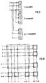
- Beim Ausführungsbeispiel nach Figur 7 sind Gruppen von jeweils x Teilkoppelfeldern auf einer Leiterplatte untergebracht. Die zyklische Vernetzung ist hier so realisiert, daß die zu den Anschlüssen der 1. Leiterplatte redundanten Leitungen (gestrichelt) auf die 2. bis (n+1). Leiterplatte verteilt werden, die der 2. Leiterplatte auf die 3. bis (n+2). Leiterplatte usw. Die redundanten Leitungen der letzten Leiterplatten werden dann auf die 1. bis n. Leiterplatte zurückgeführt. Somit kann in der Eingangsstufe und in der Ausgangsstufe nicht nur ein Teilkoppelfeld sondern eine auf einer Leiterplatte sich befindende Gruppe von x Teilkoppelfeldern ausfallen, ohne daß die Blockierungsfreiheit verloren geht. Diese zyklische Vernetzung, die bei n Anschlüssen pro Teilkoppelfeld mindestens n + 1 Leiterplatten benötigt, ist auch für eine modulare Erweiterung des Koppelfeldes von Bedeutung. In der Zwischenstufe kann dagegen wegen der Redundanz höchstens ein Teilkoppelfeld auf einer Leiterplatte untergebracht werden, da hier gegenüber einem herkömmlichen Clos-Koppelfeld nur ein Teilkoppelfeld zuviel angeschlossen und damit ausgewechselt werden kann.
- Für die Eingangs- und Ausgangsstufe können vorteilhaft gleichartige quadratische Module verwendet werden.
- Das Koppelfeld nach der Erfindung wird beispielsweise mit Koppelbausteinen der Größe 16 x 16 aufgebaut. Diese können bereits ein Teilkoppelfeld bilden oder ein Teilkoppelfeld kann aus diesen Koppelbausteinen zusammengesetzt sein
- Damit die Anzahl der Koppelpunkte und der Koppelbausteine klein ist und die Komplexität der Vernetzung überschaubar wird das Clos-Koppelfeld für 512 Anschlüsse mit 16 x 16 Modulen in der Eingangs- und Ausgangsstufe aufgebaut. Das Clos-Koppelfeld besitzt somit 64(16 x 16) Teilkoppelfelder in der Eingangs- und Ausgangsstufe und 16(64 x 64) Teilkoppelfelder in der Zwischenstufe.
- Ein redundantes Clos-Koppelfeld n x n kann gemäß Fig. 8 mit einstufigen Koppelfeldern m x m modular erweitert werden. Die Redundanz bleibt jedoch nur dann erhalten, wenn bei den einstufigen Koppelfeldern redundante Eingänge vorgesehen sind.
- Eine Möglichkeit der Erweiterung besteht darin redundante Koppelfelder parallel zu schalten (Fig. 9). Das in Fig. 9 dargestellte Koppelfeld wird aus zwei parallel geschalteten mit quadratischen Modulen aufgebauten Koppelfeldern gewonnen. Die Eingänge werden bedarfsweise unter Zwischenschaltung einer Verknüpfungslogik VL auf beide Koppelfelder KF1 und KF2 gleichmäßig verteilt und die Ausgänge über eine Verknüpfungsschaltung VS zusammengefaßt.
- Die Blockierungsfreiheit mit Redundanz bleibt unter der Voraussetzung erhalten, daß die Verknüpfungslogik VL bzw -schaltung VS nicht ausfällt
- Zur Realisierung der Koppelpunktschaltkreise der verwendeten Teilkoppelfelder gibt es die vielfältigsten Möglichkeiten, beispielsweise die Ausbildung als Ermitter- oder Differenzverstärkerstufe mit nachgeschalteter Basisstufe (EP 148 395; US 4,630,046).
Claims (6)
- Dreistufiges blockierungsfreies Clos-Koppelfeld mit einer aus mehreren Teilkoppelfeldern bestehenden Eingangsstufe, auf die die Koppelfeldeingänge verteilt sind, mit einer aus ebenfalls mehreren Teilkoppelfeldern bestehenden Ausgangsstufe und mit einer aus mehreren Teilkoppelfeldern bestehenden Zwischenstufe, dadurch gekennzeichnet, daß die Zahl der Ein- bzw. Ausgänge jedes der Teilkoppelfelder der Eingangs- bzw. Ausgangsstufe (ES, AS) in Bezug auf die Anzahl der Koppelfeldeingänge bzw. -ausgänge des jeweiligen Teilkoppelfeldes mindestens doppelt so groß gewählt ist, daß die Zwischenstufe (ZS) mindestens ein Teilkoppelfeld mehr aufweist als es für ein blockierungsfreies Koppelfeld erforderlich ist, daß die durch die Vervielfachung entstandenen n redundanten Ein- bzw. Ausgänge der Teilkoppelfelder mit nichtredundanten Koppelfeldeinbzw. -ausgängen mehrerer anderer Teilkoppelfelder der gleichen Stufe verbunden sind, und zwar so, daß die n redundanten Ein- bzw. Ausgänge eines Teilkoppelfeldes einzeln mit nichtredundanten Ein-bzw. Ausgängen von anderen Teilkoppelfeldern verbunden sind.
- Koppelfeld nach Anspruch 1, dadurch gekennzeichnet, daß jeweils eine Gruppe von Teilkoppelfeldern einer Eingangs-oder Ausgangsstufe bezüglich ihrer redundanten Ein- bzw. Ausgänge mit den nichtredundanten Ein- bzw. Ausgängen einer folgenden Gruppe von Teilkoppelfeldern dieser Stufe in zyklischer Reihenfolge verbunden ist.
- Koppelfeld nach Anspruch 2, dadurch gekennzeichnet, daß jede Gruppe von Teilkoppelfeldern der Eingangs- und Ausgangsstufe auf einer Leiterplatte untergebracht ist.
- Koppelfeld nach Anspruch 1 oder 2, dadurch gekennzeichnet, daß alle Teilkoppelfelder bzw. Gruppen von Teilkoppelfeldern mit gleichartigen Modulen aufgebaut sind.
- Koppelfeld nach einem der Ansprüche 1 bis 4, dadurch gekennzeichnet, daß Koppelfelder, deren Teilkoppelfelder nur nichtredunante Ein-bzw. Ausgänge aufweisen dadurch um redundante Eingänge erweitert sind, daß mindestens zwei solcher Koppelfelder parallel geschaltet sind.
- Koppelfeld nach einem der Ansprüche 1 bis 5, dadurch gekennzeichnet daß die Teilkoppelfelder bzw. Module quadratisch, d.h. mit gleicher Anzahl von Ein- und Ausgängen aufgebaut sind.
Priority Applications (1)
| Application Number | Priority Date | Filing Date | Title |
|---|---|---|---|
| AT88119944T ATE79208T1 (de) | 1988-01-29 | 1988-11-30 | Dreistufiges blockierungsfreies koppelfeld. |
Applications Claiming Priority (2)
| Application Number | Priority Date | Filing Date | Title |
|---|---|---|---|
| DE3802579 | 1988-01-29 | ||
| DE3802579A DE3802579A1 (de) | 1988-01-29 | 1988-01-29 | Dreistufiges blockierungsfreies koppelfeld |
Publications (3)
| Publication Number | Publication Date |
|---|---|
| EP0333922A1 EP0333922A1 (de) | 1989-09-27 |
| EP0333922B1 EP0333922B1 (de) | 1992-08-05 |
| EP0333922B2 true EP0333922B2 (de) | 1996-08-28 |
Family
ID=6346200
Family Applications (1)
| Application Number | Title | Priority Date | Filing Date |
|---|---|---|---|
| EP88119944A Expired - Lifetime EP0333922B2 (de) | 1988-01-29 | 1988-11-30 | Dreistufiges blockierungsfreies Koppelfeld |
Country Status (6)
| Country | Link |
|---|---|
| US (1) | US4983961A (de) |
| EP (1) | EP0333922B2 (de) |
| AT (1) | ATE79208T1 (de) |
| CA (1) | CA1324203C (de) |
| DE (2) | DE3802579A1 (de) |
| ES (1) | ES2034130T5 (de) |
Families Citing this family (18)
| Publication number | Priority date | Publication date | Assignee | Title |
|---|---|---|---|---|
| US5471460A (en) * | 1990-10-25 | 1995-11-28 | Nec Corporation | ATM switching system with unit switch selecting function for avoiding faulty unit switch |
| US5654695A (en) * | 1991-02-22 | 1997-08-05 | International Business Machines Corporation | Multi-function network |
| LU87976A1 (de) * | 1991-03-14 | 1992-04-15 | Siemens Ag | Dreistufige,zumindest gedoppelte atm-koppelanordnung |
| US5317310A (en) * | 1992-05-14 | 1994-05-31 | Alcatel Network Systems, Inc. | Method and system for selecting an optimal rearrangement sequence for a cross-connect communication matrix |
| US5371786A (en) * | 1993-09-29 | 1994-12-06 | At&T Bell Corp. | Electronic cross-connect system |
| SE506922C2 (sv) | 1995-10-09 | 1998-03-02 | Ericsson Telefon Ab L M | Skyddskopplingarrangemang vid kommunikationsväljarsystem |
| US6087958A (en) * | 1997-07-14 | 2000-07-11 | Arzt; Lawrence J. | Multi-stage routing switchers with sequential and non-repetitive distributive circuit interconnections |
| US6614904B1 (en) * | 2000-08-09 | 2003-09-02 | Alcatel | Apparatus and method for effecting a communication arrangement between switch arrays |
| CN100484258C (zh) * | 2001-08-31 | 2009-04-29 | 艾利森电话股份有限公司 | 可缩放的模块化的严格无阻塞的电光交叉连接核心 |
| WO2003019879A1 (en) * | 2001-08-31 | 2003-03-06 | Telefonaktiebolaget Lm Ericsson | Three-stage non-blocking fault tolerant cross-connect architecture |
| US7313135B2 (en) * | 2002-01-31 | 2007-12-25 | Mosaid Technologies, Inc. | Trunking in a matrix |
| GB2430326A (en) * | 2005-09-16 | 2007-03-21 | Tyco Electronics Raychem Nv | Cross connect device comprising a plurality of sparse cross bars |
| US20070080731A1 (en) * | 2005-10-11 | 2007-04-12 | Kim Jung P | Duty cycle corrector |
| US20080143473A1 (en) * | 2006-12-19 | 2008-06-19 | Kevin Wilson | Digital Cross-Connect Path Selection Method |
| US7804825B2 (en) * | 2006-12-20 | 2010-09-28 | Kevin Wilson | Matrix expansion lattice |
| US7956668B2 (en) * | 2006-12-20 | 2011-06-07 | Kevin Wilson | Spectral predictive switching device activation |
| EP2680516A1 (de) * | 2006-12-19 | 2014-01-01 | Kevin Wilson | Matrixexpansionsgitter |
| US8369321B2 (en) * | 2010-04-01 | 2013-02-05 | Juniper Networks, Inc. | Apparatus and methods related to the packaging and cabling infrastructure of a distributed switch fabric |
Family Cites Families (13)
| Publication number | Priority date | Publication date | Assignee | Title |
|---|---|---|---|---|
| DE1130482B (de) * | 1961-03-07 | 1962-05-30 | Standard Elektrik Lorenz Ag | Zwischenleitungsanordnung fuer die Koppelblocks zweier oder mehrerer Koppelstufen inFernmelde-, insbesondere Fernsprechvermittlungsanlagen |
| US3582560A (en) * | 1968-08-02 | 1971-06-01 | Communications & Systems Inc | Multistage telephone switching system for different priority users |
| DE2424727A1 (de) * | 1974-05-21 | 1975-12-04 | Telefonbau & Normalzeit Gmbh | Verfahren zur erweiterung von koppeleinheiten, insbesondere fuer mischkoppelfelder in fernmeldevermittlungsanlagen |
| US3978291A (en) * | 1974-09-09 | 1976-08-31 | Bell Telephone Laboratories, Incorporated | Automated main distributing frame system |
| JPS5726955A (en) * | 1980-07-25 | 1982-02-13 | Hitachi Ltd | Backup control system |
| IT1159090B (it) * | 1982-09-01 | 1987-02-25 | Italtel Spa | Rete di commutazione pcm ridondata a ripartizione di traffico |
| US4605928A (en) * | 1983-10-24 | 1986-08-12 | International Business Machines Corporation | Fault-tolerant array of cross-point switching matrices |
| EP0148395B1 (de) * | 1984-01-05 | 1991-02-06 | ANT Nachrichtentechnik GmbH | Breitbandkoppelfeld in Matrixform |
| US4654842A (en) * | 1984-08-02 | 1987-03-31 | Coraluppi Giorgio L | Rearrangeable full availability multistage switching network with redundant conductors |
| US4862161A (en) * | 1985-01-24 | 1989-08-29 | Ant Nachrichtentechnik Gmbh | Three-stage coupling arrangement |
| EP0240580B2 (de) * | 1986-04-03 | 1994-11-17 | ANT Nachrichtentechnik GmbH | Dreistufige Koppelanordnung |
| GB2188813B (en) * | 1986-04-01 | 1990-03-14 | Stc Plc | Switching network |
| US4807280A (en) * | 1987-09-18 | 1989-02-21 | Pacific Bell | Cross-connect switch |
-
1988
- 1988-01-29 DE DE3802579A patent/DE3802579A1/de not_active Withdrawn
- 1988-11-30 AT AT88119944T patent/ATE79208T1/de not_active IP Right Cessation
- 1988-11-30 DE DE8888119944T patent/DE3873519D1/de not_active Expired - Lifetime
- 1988-11-30 ES ES88119944T patent/ES2034130T5/es not_active Expired - Lifetime
- 1988-11-30 EP EP88119944A patent/EP0333922B2/de not_active Expired - Lifetime
-
1989
- 1989-01-27 CA CA000589307A patent/CA1324203C/en not_active Expired - Fee Related
- 1989-01-27 US US07/302,465 patent/US4983961A/en not_active Expired - Lifetime
Also Published As
| Publication number | Publication date |
|---|---|
| DE3802579A1 (de) | 1989-08-10 |
| ES2034130T5 (es) | 1996-12-16 |
| ATE79208T1 (de) | 1992-08-15 |
| CA1324203C (en) | 1993-11-09 |
| ES2034130T3 (es) | 1993-04-01 |
| EP0333922B1 (de) | 1992-08-05 |
| DE3873519D1 (de) | 1992-09-10 |
| US4983961A (en) | 1991-01-08 |
| EP0333922A1 (de) | 1989-09-27 |
Similar Documents
| Publication | Publication Date | Title |
|---|---|---|
| EP0333922B2 (de) | Dreistufiges blockierungsfreies Koppelfeld | |
| DE69914344T2 (de) | Nichtblockierender optischer schalterkern mit optimierter schaltarchitektur basierend auf reziprozitätsbedingungen | |
| DE3781807T2 (de) | Schaltbare netzwerke. | |
| DE2249371C2 (de) | Zeitvielfachvermittlungsanlage | |
| DE60114534T2 (de) | Kondensatorarray-d/a-wandler mit einem temperaturmessgerät-decoder sowie kondensatorray | |
| DE69023796T2 (de) | Verfahren und System für Netzumordnung. | |
| DE2916065C2 (de) | Datenverarbeitungseinrichtung | |
| EP0399139B1 (de) | Verfahren zur Erweiterung eines dreistufigen regelmässigen Koppelfeldes | |
| DE4415016A1 (de) | Verfahren zum Betreiben eines Koppelnetzes sowie Koppelnetz und Vermittlungsstelle dafür | |
| DE3884537T2 (de) | Kommunikationsvermittlungselement. | |
| EP0039077B1 (de) | Zeitmultiplexkoppelfeld | |
| DE2728078A1 (de) | Anschlusschaltung mit zeit- und raumkopplung und fernsprech-waehlvermittlungsanordnung mit einer solchen anschlusschaltung | |
| EP0270185B1 (de) | Breitband-Raumvielfachkoppelfeld mit Zwischenleitungsführung in einer Leiterplatte mit mehrlagigen Leiterbahnen in Mikrostrip-Technik | |
| EP0219848A2 (de) | Breitbandsignal-Raumkoppeleinrichtung | |
| DE3640849C2 (de) | ||
| DE2910253C2 (de) | Indirekt gesteuerte Vermittlungsanlage, insbesondere Fernsprechvermittlungsanlage | |
| DE2250516B2 (de) | Fernmeldenetzwerk mit sternfoermiger struktur | |
| DE2503102C3 (de) | ||
| DE2602561A1 (de) | Zeitmultiplexkoppelfeld | |
| DE2542579A1 (de) | Koppelfeld fuer fernmeldevermittlungssysteme | |
| DE4021587A1 (de) | Integrierter koppelfeldbaustein | |
| DE1562126B2 (de) | Schaltungsanordnung für ein Koppelnetz für Fernmelde-, insbesondere Fernsprechvermittlungsanlagen | |
| DE4333515C2 (de) | Flexible Auswahlschaltung | |
| DE2148995C3 (de) | Schaltungsanordnung für ein mit einem Wegesuchnetzwerk ausgestattetes, mehrstufiges Koppelfeld in Fernmelde-, insbesondere Fernsprechvermittlungsanlagen | |
| DE2659178C2 (de) | Koppelanordnung, insbesondere für den Anschluß von Zeitmultiplexleitungen |
Legal Events
| Date | Code | Title | Description |
|---|---|---|---|
| PUAI | Public reference made under article 153(3) epc to a published international application that has entered the european phase |
Free format text: ORIGINAL CODE: 0009012 |
|
| AK | Designated contracting states |
Kind code of ref document: A1 Designated state(s): AT BE CH DE ES FR GB IT LI NL SE |
|
| 17P | Request for examination filed |
Effective date: 19891013 |
|
| 17Q | First examination report despatched |
Effective date: 19911210 |
|
| GRAA | (expected) grant |
Free format text: ORIGINAL CODE: 0009210 |
|
| AK | Designated contracting states |
Kind code of ref document: B1 Designated state(s): AT BE CH DE ES FR GB IT LI NL SE |
|
| REF | Corresponds to: |
Ref document number: 79208 Country of ref document: AT Date of ref document: 19920815 Kind code of ref document: T |
|
| ITF | It: translation for a ep patent filed | ||
| GBT | Gb: translation of ep patent filed (gb section 77(6)(a)/1977) | ||
| REF | Corresponds to: |
Ref document number: 3873519 Country of ref document: DE Date of ref document: 19920910 |
|
| ET | Fr: translation filed | ||
| REG | Reference to a national code |
Ref country code: ES Ref legal event code: FG2A Ref document number: 2034130 Country of ref document: ES Kind code of ref document: T5 |
|
| PLBI | Opposition filed |
Free format text: ORIGINAL CODE: 0009260 |
|
| 26 | Opposition filed |
Opponent name: SIEMENS AKTIENGESELLSCHAFT, BERLIN UND MUENCHEN Effective date: 19930505 |
|
| NLR1 | Nl: opposition has been filed with the epo |
Opponent name: SIEMENS AG |
|
| PGFP | Annual fee paid to national office [announced via postgrant information from national office to epo] |
Ref country code: NL Payment date: 19931130 Year of fee payment: 6 |
|
| REG | Reference to a national code |
Ref country code: GB Ref legal event code: 746 Effective date: 19940322 |
|
| REG | Reference to a national code |
Ref country code: FR Ref legal event code: DL |
|
| EAL | Se: european patent in force in sweden |
Ref document number: 88119944.2 |
|
| PG25 | Lapsed in a contracting state [announced via postgrant information from national office to epo] |
Ref country code: NL Effective date: 19950601 |
|
| NLV4 | Nl: lapsed or anulled due to non-payment of the annual fee | ||
| PLAW | Interlocutory decision in opposition |
Free format text: ORIGINAL CODE: EPIDOS IDOP |
|
| PUAH | Patent maintained in amended form |
Free format text: ORIGINAL CODE: 0009272 |
|
| STAA | Information on the status of an ep patent application or granted ep patent |
Free format text: STATUS: PATENT MAINTAINED AS AMENDED |
|
| 27A | Patent maintained in amended form |
Effective date: 19960828 |
|
| AK | Designated contracting states |
Kind code of ref document: B2 Designated state(s): AT BE CH DE ES FR GB IT LI NL SE |
|
| REG | Reference to a national code |
Ref country code: CH Ref legal event code: AEN Free format text: AUFRECHTERHALTUNG DES PATENTES IN GEAENDERTER FORM |
|
| ITF | It: translation for a ep patent filed | ||
| GBTA | Gb: translation of amended ep patent filed (gb section 77(6)(b)/1977) |
Effective date: 19891224 |
|
| ET3 | Fr: translation filed ** decision concerning opposition | ||
| REG | Reference to a national code |
Ref country code: ES Ref legal event code: DC2A Kind code of ref document: T5 Effective date: 19961015 |
|
| PGFP | Annual fee paid to national office [announced via postgrant information from national office to epo] |
Ref country code: AT Payment date: 20001113 Year of fee payment: 13 |
|
| PGFP | Annual fee paid to national office [announced via postgrant information from national office to epo] |
Ref country code: CH Payment date: 20001128 Year of fee payment: 13 |
|
| PG25 | Lapsed in a contracting state [announced via postgrant information from national office to epo] |
Ref country code: LI Free format text: LAPSE BECAUSE OF NON-PAYMENT OF DUE FEES Effective date: 20011130 Ref country code: CH Free format text: LAPSE BECAUSE OF NON-PAYMENT OF DUE FEES Effective date: 20011130 Ref country code: AT Free format text: LAPSE BECAUSE OF NON-PAYMENT OF DUE FEES Effective date: 20011130 |
|
| REG | Reference to a national code |
Ref country code: GB Ref legal event code: IF02 |
|
| REG | Reference to a national code |
Ref country code: CH Ref legal event code: PL |
|
| PGFP | Annual fee paid to national office [announced via postgrant information from national office to epo] |
Ref country code: GB Payment date: 20021021 Year of fee payment: 15 |
|
| PGFP | Annual fee paid to national office [announced via postgrant information from national office to epo] |
Ref country code: SE Payment date: 20021106 Year of fee payment: 15 |
|
| PGFP | Annual fee paid to national office [announced via postgrant information from national office to epo] |
Ref country code: FR Payment date: 20021108 Year of fee payment: 15 |
|
| PGFP | Annual fee paid to national office [announced via postgrant information from national office to epo] |
Ref country code: ES Payment date: 20021127 Year of fee payment: 15 |
|
| PGFP | Annual fee paid to national office [announced via postgrant information from national office to epo] |
Ref country code: DE Payment date: 20021205 Year of fee payment: 15 |
|
| PGFP | Annual fee paid to national office [announced via postgrant information from national office to epo] |
Ref country code: BE Payment date: 20030117 Year of fee payment: 15 |
|
| PG25 | Lapsed in a contracting state [announced via postgrant information from national office to epo] |
Ref country code: GB Free format text: LAPSE BECAUSE OF NON-PAYMENT OF DUE FEES Effective date: 20031130 Ref country code: BE Free format text: LAPSE BECAUSE OF NON-PAYMENT OF DUE FEES Effective date: 20031130 |
|
| PG25 | Lapsed in a contracting state [announced via postgrant information from national office to epo] |
Ref country code: SE Free format text: LAPSE BECAUSE OF NON-PAYMENT OF DUE FEES Effective date: 20031201 Ref country code: ES Free format text: LAPSE BECAUSE OF NON-PAYMENT OF DUE FEES Effective date: 20031201 |
|
| BERE | Be: lapsed |
Owner name: *ANT NACHRICHTENTECHNIK G.M.B.H. Effective date: 20031130 |
|
| PG25 | Lapsed in a contracting state [announced via postgrant information from national office to epo] |
Ref country code: DE Free format text: LAPSE BECAUSE OF NON-PAYMENT OF DUE FEES Effective date: 20040602 |
|
| GBPC | Gb: european patent ceased through non-payment of renewal fee |
Effective date: 20031130 |
|
| PG25 | Lapsed in a contracting state [announced via postgrant information from national office to epo] |
Ref country code: FR Free format text: LAPSE BECAUSE OF NON-PAYMENT OF DUE FEES Effective date: 20040730 |
|
| EUG | Se: european patent has lapsed | ||
| REG | Reference to a national code |
Ref country code: FR Ref legal event code: ST |
|
| REG | Reference to a national code |
Ref country code: ES Ref legal event code: FD2A Effective date: 20031201 |
|
| PG25 | Lapsed in a contracting state [announced via postgrant information from national office to epo] |
Ref country code: IT Free format text: LAPSE BECAUSE OF NON-PAYMENT OF DUE FEES;WARNING: LAPSES OF ITALIAN PATENTS WITH EFFECTIVE DATE BEFORE 2007 MAY HAVE OCCURRED AT ANY TIME BEFORE 2007. THE CORRECT EFFECTIVE DATE MAY BE DIFFERENT FROM THE ONE RECORDED. Effective date: 20051130 |