EP0332217B1 - Dünnfilm-Transistor zum Betrieb für hohe Spannungen und dessen Herstellungsverfahren - Google Patents
Dünnfilm-Transistor zum Betrieb für hohe Spannungen und dessen Herstellungsverfahren Download PDFInfo
- Publication number
- EP0332217B1 EP0332217B1 EP89104322A EP89104322A EP0332217B1 EP 0332217 B1 EP0332217 B1 EP 0332217B1 EP 89104322 A EP89104322 A EP 89104322A EP 89104322 A EP89104322 A EP 89104322A EP 0332217 B1 EP0332217 B1 EP 0332217B1
- Authority
- EP
- European Patent Office
- Prior art keywords
- gate electrode
- film
- insulator
- semiconductor film
- field effect
- Prior art date
- Legal status (The legal status is an assumption and is not a legal conclusion. Google has not performed a legal analysis and makes no representation as to the accuracy of the status listed.)
- Expired - Lifetime
Links
Images


Classifications
-
- H—ELECTRICITY
- H10—SEMICONDUCTOR DEVICES; ELECTRIC SOLID-STATE DEVICES NOT OTHERWISE PROVIDED FOR
- H10D—INORGANIC ELECTRIC SEMICONDUCTOR DEVICES
- H10D30/00—Field-effect transistors [FET]
- H10D30/60—Insulated-gate field-effect transistors [IGFET]
- H10D30/67—Thin-film transistors [TFT]
- H10D30/6728—Vertical TFTs
-
- Y—GENERAL TAGGING OF NEW TECHNOLOGICAL DEVELOPMENTS; GENERAL TAGGING OF CROSS-SECTIONAL TECHNOLOGIES SPANNING OVER SEVERAL SECTIONS OF THE IPC; TECHNICAL SUBJECTS COVERED BY FORMER USPC CROSS-REFERENCE ART COLLECTIONS [XRACs] AND DIGESTS
- Y10—TECHNICAL SUBJECTS COVERED BY FORMER USPC
- Y10S—TECHNICAL SUBJECTS COVERED BY FORMER USPC CROSS-REFERENCE ART COLLECTIONS [XRACs] AND DIGESTS
- Y10S148/00—Metal treatment
- Y10S148/082—Ion implantation FETs/COMs
-
- Y—GENERAL TAGGING OF NEW TECHNOLOGICAL DEVELOPMENTS; GENERAL TAGGING OF CROSS-SECTIONAL TECHNOLOGIES SPANNING OVER SEVERAL SECTIONS OF THE IPC; TECHNICAL SUBJECTS COVERED BY FORMER USPC CROSS-REFERENCE ART COLLECTIONS [XRACs] AND DIGESTS
- Y10—TECHNICAL SUBJECTS COVERED BY FORMER USPC
- Y10S—TECHNICAL SUBJECTS COVERED BY FORMER USPC CROSS-REFERENCE ART COLLECTIONS [XRACs] AND DIGESTS
- Y10S148/00—Metal treatment
- Y10S148/15—Silicon on sapphire SOS
Definitions
- the present invention relates to a thin-film transistor operable at a high voltage and a method for manufacturing the same.
- MOS-type field effect transistors A miniaturization of MOS-type field effect transistors becomes important, as the integration density increases.
- a MOS-type thin-film field effect transistor was devised to use a step portion as its channel portion (see IEEE Transactions on Electron Devices, Vol. ED-32, No. 2 (February 1985), pages 258 to 281 and US-A-4 633 284).
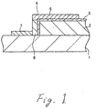
- the structure of such thin-film transistor will be explained with reference to Fig. 1 showing a sectional view of the prior art transistor.
- the MOS-type thin-film transistor is formed on a first insulating film 1 which may be a thin film formed on other substrate or a surface portion of an insulating substrate.
- a gate electrode 2 is formed on the first insulating film 1 with a polycrystalline silicon.
- a second insulating film 3 is formed on the upper and side surfaces of the gate electrode 2 so as to be used as a gate insulating layer.
- a polycrystalline silicon film 4 is deposited over the step portion at the edge of the gate electrode 2 so as to continuously contact with the surface of the first insulating film 1 and side and upper surfaces of the second insulating film 3.
- Source region 6 and drain region 7 are formed by implanting impulities.
- the vertical portion of the polycrystalline silicon layer 4 functions as a channel region 8.
- Such MOS thin-film transistor is formed by using ion-implantation to form the source and drain regions 6 and 7.
- the channel region 8 has the same thickness as the polycrystalline silicon film 4.
- the gate electrode 2 has a small thickness. Therefore, the drain region 7 positions very close to the source region 6, resulting in a small withstand voltage applicable to the drain region and a large leakage current flowing between the source and drain regions through the channel region.
- an primary object of the present invention to provide a MOS-type thin-film field effect transistor having a miniaturized structure, a large withstand voltage and a small leakage current.
- a MOS-type thin-film field effect transistor consisted of an insulating body having a main surface, a gate electrode formed on the main surface, the gate electrode having a side surface and an upper surface, an insulating film formed to cover the side and upper surfaces of the gate electrode, a silicon layer continuously formed in contact with the insulating film on the upper and side surfaces of the gate electrode and extended above the insulating body exposed from the gate electrode and the insulating film to form a cranked portion, a side-wall insulator formed on the outer-side of the silicon layer at the cranked portion, and the side-wall insulator having a bottom contacting the silicon layer directly above the insulating body and a side contacting the silicon layer positioning in parallel with the side surface of the gate electrode, a portion of the silicon layer positioning in parallel with the upper surface of the gate electrode being used as one of source and drain regions and another portion of the silicon layer positioning directly above and exposing from the side-wall insulator being used as the
- a method for manufacturing a MOS-type thin-film field effect transistor which includes steps of forming a gate electrode on an insulating body, the gate electrode having side and upper surfaces, forming an insulating film on the side and upper surfaces of the gate electrode, forming a silicon layer on the insulating film to extend directly above the insulating body, the formed silicon layer having a cranked shape composed of a first portion positioning directly above the insulating body, a second portion positioning in parallel with the side surface of the gate electrode and a third portion positioning above the upper surface of the gate electrode, forming a side-wall insulator having a bottom contacting with the first portion of the silicon layer and a side face contacting with the second portion of the silicon layer, introducing impurity into the silicon layer with use of the side-wall insulator as a mask to form source and drain regions in the silicon layer.
- the first aspect of the present invention has an offset region in the silicon layer positioning under and in contact with the bottom of the side-wall insulator.
- This offset region positioned between the drain region and the channel region which is a portion of the silicon layer formed in parallel with the side surface of the gate electrode. Due to the existence of the offset region, the drain withstand voltage is improved to have an increased value. A leakage current which flows between the source and drain regions through the channel region is minimized.
- the channel region and the offset region are automatically formed by introducing impurity using the side-wall insulator as a mask. Any process requiring a precise alignment is not involved in the manufacturing procedure.
- a first preferred embodiment shown in Fig. 2 is formed on an insulating body 1 which may be an insulating substrate or a SiO2 film formed on a substrate such as Si.
- the polycrystalline silicon gate electrode 12 is covered with an insulating film 13 of SiO2 having a thickness of 300 ⁇ which is, for example, formed by thermal oxidation.
- the insulating film 13 is alternatively formed by vapor phase deposition.
- a polycrystalline silicon film 14 having a thickness of 1,000 ⁇ is formed on the insulating film 13 and is extended to the insulating body 11.
- the formed silicon film 14 has a cranked shape deposited along the upper surface of insulating body 11, the vertical side surface of the insulating film 13 and the horizontal upper surface of the insulating film 13.
- a side-wall insulator 15 is formed on the silicon layer 14 at a bent portion connecting a horizontal portion on the insulating body 11 and a vertical portion contacting with the insulating film 13 on the vertical side of the gate electrode 12.
- the side-wall insulator 15 has a bottom width of 2,000 ⁇ to 5,000 ⁇ and a hight same as the vertical hight of the vertical portion of the silicon layer 14.
- the source and drain regions 16 and 17 are formed by introducing impurity into the silicon layer 14 with use of the side-wall insulator 15 as a mask.
- the impurity may be introduced by ion-implantation, solid-phase diffusion or vapor-phase diffusion.
- the impurity is, for example, boron and its concentration is, for example, 1 x 1020 cm ⁇ 3.
- the source region 16 is a portion of the silicon layer 14 positioning upon the gate electrode 12.
- the drain region 17 is in a portion of the silicon layer 14 positioning on the insulating body 11.
- a channel region 18 is the vertical portion of the silicon layer 14. In the portion of the silicon layer 14 positioning on the insulating body 11, an offset region 19 exists between the drain region 17 and the channel region 18. It positions under the side-wall insulator 15 and is prevented from introducing impurity by the side-wall insulator 15.
- the drain region 17 Due to the existence of the offset region 19, the drain region 17 is kept distant from the source region 16 and the gate electrode 12. Therefore, the electric field between the drain region 17 and the source region 16 and between the drain region 17 and the gate electrode 12 are reduced. Thus, a high voltage can be applied to the drain region 17 to allow a high power operation. By similar reason, the leakage current flowing through the channel region 18 and the offset region 19 is reduced to a very small value.
- the channel and offset regions 18 and 19 are passivated by the side-wall insulator 15. Therefore, a very stable operation can be expected.
- the insulating body 11 is an SiO2 film formed on a silicon substrate (not shown).
- a polycrystalline silicon film is deposited on the insulating body 11 to have a thickness of 5,000 ⁇ and is doped with impurity ions of phosphorous by thermal diffusion.
- a photo-etching process is subjected to the polycrystalline silicon film to form a gate electrode 12.
- the surface of the gate electrode 12 is converted into an insulating film 13 of SiO2 by thermal oxidation of polycrystalline silicon.
- the preferable thickness of the insulating film 13 is 300 ⁇ .
- the insulating film 13 may be alternatively deposited by vapor-phase deposition.
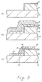
- the polycrystalline silicon film is shaped to have a cranked form, as shown in Fig. 3(b), by another photo-etching process.
- the cranked form is automatically obtained by using the edge portion of the gate electrode 12.
- the shaped silicon film 14 has an upper horizontal portion positioning above the gate electrode 12, a vertical portion positioning in parallel with the side edge of the gate electrode 12 and a lower horizontal portion positioning on the exposed surface of the insulating body 11.
- An insulator 10 such as SiO2 is deposited over the whole surface with a thickness of 2,000 ⁇ by vapor-phase deposition.
- the insulator 10 is anisotropically etched by a reactive ion-etching process to form a side-wall insulator 15 shown in Fig. 3(c).
- the side-wall insulator 15 has a bottom having a width of 2,000 ⁇ contacting with the lower horizontal portion of the shaped silicon film 14 and has a vertical side contacting the vertical portion of the shaped silicon film 14.
- Impurity ions of boron are implanted into the silicon film 14 using the side-wall insulator 15 as a mask.
- the preferable impurity concentration of the implanted regions is about 1 x 1020 cm ⁇ 3.
- the upper horizontal portion of the shaped silicon film 14 is thus doped and used as a source region 16.
- a part of the lower horizontal portion of the shaped silicon film 14 which is exposed from the side-wall insulator 15 is also doped to be used as a drain region.
- the other part of the lower horizontal portion of the shaped silicon film 14 which positions under the side-wall insulator 15 is undoped to be used as an offset region 19.
- the vertical portion of the shaped silicon film 14 is a channel region of which conductivity is controlled by the gate electrode 12.
- the positioning of the source, drain, offset and channel regions are defined by self-alignment. Any precise control of positioning is not required to facilitate the manufacturing process.
- a passivation film 20 of SiO2 is covered over the whole structure which has a similar structure to a MOS-type thin-film field effect transistor shown in Fig. 2. That is, a polycrystalline silicon gate electrode 22 is formed on an insulating body and is covered with an insulator film 23 of oxidized SiO2. A cranked shape silicon film is formed at the edge of the gate electrode 22 to have a lower horizontal portion on the insulating body 21, a vertical portion at the side edge of the gate electrode 22 and an upper horizontal portion on the gate electrode 22. A side-wall insulator 25 is formed on the corner of the cranked shape silicon film between the lower horizontal portion and the vertical portion.
- the passivation film 20 is formed by applying a solution containing silica and boron over the whole surface and then being subjected to a heat treatment to convert the solution into a boron-doped SiO2 film. During this heat treatment, the doped boron diffuses into the silicon film to form a source region 26 and the drain region 27.
- the side-wall insulator 25 acts as a mask for diffusion of boron.
- the SiO2 film 20 is usable as a passivation film or an inter-layer insulating film on which wiring layer is formed.
- the impurity diffusion for source and drain regions and the formation of the passivation or inter-layer insulating film are simultaneously achieved, resulted in a save of process steps.
- the insulating films 13 and 23 may be formed by vapor-phase deposition.
- the insulating films 13 and 23 extend over the insulating body 11 and 21, respectively, on which the drain regions 17 and 27 and the offset regions 19 and 29 are formed.
- the similar effects and advantages to the first and second embodiments of the present invention can be obtained in this modification.
- the introduction of impurity into the source and drain regions can be performed by diffusion from vapor-phase.
- the length of the offset region that is, a width of the bottom of the side-wall insulator is arbitrarily selected but is effective on operation if it is from 2,000 ⁇ to 5,000 ⁇ .
- Other dimensions such as thickness, length and width of the gate electrode 12, 22 and source, channel offset and drain regions may be arbitrarily selected.
Landscapes
- Thin Film Transistor (AREA)
- Insulated Gate Type Field-Effect Transistor (AREA)
Claims (8)
- Dünnfilm-Feldeffekttransistor vom MOS-Typ, bestehend aus:
einem Substrat (11) mit einer isolierenden Hauptfläche; einer Gate-Elektrode (12), die auf der isolierenden Hauptfläche ausgebildet ist, mit einer oberen Flache und einer Seitenfläche an einem Rand;
einem isolierenden Film (13), der wenigstens die oberen und Seitenflachen der Gate-Elektrode bedeckt;
einem Halbleiterfilm (14), mit drei fortlaufenden Abschnitten (16, 17, 18, 19) erster, zweiter und dritter Abschnitte, wobei der erste Abschnitt (16) oberhalb der oberen Fläche der Gate-Elektrode positioniert ist, der zweite Abschnitt (18) in Kontakt mit dem Isolierfilm an der Seitenfläche der Gateelektrode ausgebildet ist;
wobei der Feldeffekttransistor
dadurch gekennzeichnet ist, daß der dritte Abschnitt (17, 19) oberhalb des Substrats ohne dazwischenliegende Gate-Elektrode angeordnet ist; und weiterhin aufweist
einen Seitenwand-Isolator (15), der auf einem Teil (19) des dritten Abschnittes des Halbleiterfilms geformt ist und eine dritte Seitenfläche hat, die den zweiten Abschnitt des Halbleiterfilms kontaktiert; und
Source- und Drainbereiche, die durch Dotieren mit Fremdatomen in den ersten Abschnitt und einen anderen Teil (17) des dritten Abschnittes des Halbleiterfilms gebildet sind, wobei der Teil und der andere Teil des dritten Abschnittes miteinander in Kontakt sind. - Dünnfilm-Feldeffekttransistor vom MOS-Typ nach Anspruch 1,
dadurch gekennzeichnet, daß die Gateelektrode und der Halbleiterfilm aus polykristallinem Silizium gebildet sind. - Dünnfilm-Feldeffekttransistor vom MOS-Typ nach Anspruch 2,
dadurch gekennzeichnet, daß der Seitenwandisolator einen Boden hat, der den Teil des dritten Abschnittes des Halbleiterfilms kontaktiert, wobei der Boden eine Breite im Bereich von 200 nm (2000 Å) bis 500 mn (5000 Å) hat. - Dünnfilm-Feldeffekttransistor vom MOS-Typ nach Anspruch 2,
dadurch gekennzeichnet, daß der Feldeffekttransistor weiterhin aufweist eine Isolatorabdeckung, die den Halbleiterfilm und den Seitenwandisolator abdeckt, wobei die Isolatorabdeckung Fremdatome enthält, die die gleichen sind, wie diejenigen, mit welchen die Source- und Drainbereiche dotiert sind. - Verfahren zum Herstellen eines Feldeffekttransistors vom MOS-Typ, mit den Arbeitsschritten:
Bilden einer Gateelektrode an einer isolierenden Hauptfläche eines Substrats;
Bilden eines isolierenden Films auf wenigstens den oberen und seitlichen Flächen der Gate-Elektrode;
Bilden eines Halbleiterfilms mit fortlaufenden ersten, zweiten und dritten Abschnitten, wobei der erste Abschnitt auf dem isolierenden Film an der oberen Fläche der Gate-Elektrode ausgebildet wird, der zweite Abschnitt in Kontakt mit dem isolierenden Film an der seitlichen Fläche der Gate-Elektrode und der dritte Abschnitt auf dem Substrat ohne dazwischenliegende Gate-Elektrode ausgebildet wird;
Bilden eines Seitenwand-Isolators mit einem Boden und einer seitlichen Fläche, wobei der Boden einen Teil des dritten Abschnittes des Halbleiterfilms kontaktiert und die seitliche Fläche des Seitenwandisolators den zweiten Abschnitt des Halbleiterfilms kontaktiert; und Dotieren des vom Seitenwandisolator nicht gedeckten Halbleiterfilms mit Fremdatomen unter Verwendung des Seitenwandisolators als Maske, um Drain- und Source-Bereiche zu bilden. - Verfahren zum Herstellen eines Feldeffekttransistors vom MOS-Typ nach Anspruch 5,
dadurch gekennzeichnet, daß der Schritt Dotieren mit Fremdatomen ein Ionen-Implantationsprozeß ist, bei dem die Fremdatome in den Halbleiterfilm, welcher von dem Seitenwandisolator nicht bedeckt ist, unter Verwendung des Seitenwandisolators als Maske, implantiert werden. - Verfahren zum Herstellen eines Feldeffekttransistors vom MOS-Typ nach Anspruch 5,
dadurch gekennzeichnet, daß der Schritt Dotieren mit Fremdatomen durchgeführt wird, indem der Halbleiterfilm und der Seitenwandisolator mit einem Isolator abgedeckt werden, der die Fremdatome enthält; und dann einer Wärmebehandlung unterzogen wird, um die Fremdatome aus dem Isolator in den vom Seitenwandisolator nicht bedeckten Halbleiterfilm einzuführen. - Verfahren zum Herstellen eines Feldeffekttransistors vom MOS-Typ nach Anspruch 7,
dadurch gekennzeichnet,
daß der Isolator eine Lösung ist, die Silizium und die Fremdatome enthält, und durch die Wärmebehandlung in einen Isolator in fester Phase umgewandelt wird.
Applications Claiming Priority (2)
| Application Number | Priority Date | Filing Date | Title |
|---|---|---|---|
| JP57422/88 | 1988-03-11 | ||
| JP63057422A JPH01231376A (ja) | 1988-03-11 | 1988-03-11 | 薄膜トランジスタおよびその製造方法 |
Publications (3)
| Publication Number | Publication Date |
|---|---|
| EP0332217A2 EP0332217A2 (de) | 1989-09-13 |
| EP0332217A3 EP0332217A3 (en) | 1990-09-19 |
| EP0332217B1 true EP0332217B1 (de) | 1993-12-29 |
Family
ID=13055215
Family Applications (1)
| Application Number | Title | Priority Date | Filing Date |
|---|---|---|---|
| EP89104322A Expired - Lifetime EP0332217B1 (de) | 1988-03-11 | 1989-03-10 | Dünnfilm-Transistor zum Betrieb für hohe Spannungen und dessen Herstellungsverfahren |
Country Status (4)
| Country | Link |
|---|---|
| US (2) | US5001540A (de) |
| EP (1) | EP0332217B1 (de) |
| JP (1) | JPH01231376A (de) |
| DE (1) | DE68911715T2 (de) |
Families Citing this family (28)
| Publication number | Priority date | Publication date | Assignee | Title |
|---|---|---|---|---|
| US5181088A (en) * | 1988-09-14 | 1993-01-19 | Kabushiki Kaisha Toshiba | Vertical field effect transistor with an extended polysilicon channel region |
| US5801396A (en) * | 1989-01-18 | 1998-09-01 | Stmicroelectronics, Inc. | Inverted field-effect device with polycrystalline silicon/germanium channel |
| US5770892A (en) * | 1989-01-18 | 1998-06-23 | Sgs-Thomson Microelectronics, Inc. | Field effect device with polycrystalline silicon channel |
| US5602403A (en) * | 1991-03-01 | 1997-02-11 | The United States Of America As Represented By The Secretary Of The Navy | Ion Implantation buried gate insulator field effect transistor |
| JP2602132B2 (ja) * | 1991-08-09 | 1997-04-23 | 三菱電機株式会社 | 薄膜電界効果素子およびその製造方法 |
| JPH0555527A (ja) * | 1991-08-28 | 1993-03-05 | Nippon Steel Corp | 半導体装置 |
| KR950001159B1 (ko) * | 1991-12-27 | 1995-02-11 | 삼성전자 주식회사 | 반도체 메모리장치의 박막트랜지스터 및 그 제조방법 |
| JPH05183164A (ja) * | 1991-12-28 | 1993-07-23 | Nec Corp | 半導体素子 |
| US5173754A (en) * | 1992-02-03 | 1992-12-22 | Micron Technology, Inc. | Integrated circuit device with gate in sidewall |
| US5324960A (en) * | 1993-01-19 | 1994-06-28 | Motorola, Inc. | Dual-transistor structure and method of formation |
| US5374572A (en) * | 1993-07-22 | 1994-12-20 | Motorola, Inc. | Method of forming a transistor having an offset channel section |
| US5510278A (en) * | 1994-09-06 | 1996-04-23 | Motorola Inc. | Method for forming a thin film transistor |
| US5716879A (en) * | 1994-12-15 | 1998-02-10 | Goldstar Electron Company, Ltd. | Method of making a thin film transistor |
| US5700727A (en) | 1995-07-24 | 1997-12-23 | Micron Technology, Inc. | Method of forming a thin film transistor |
| US5640023A (en) * | 1995-08-31 | 1997-06-17 | Sgs-Thomson Microelectronics, Inc. | Spacer-type thin-film polysilicon transistor for low-power memory devices |
| US5574294A (en) * | 1995-12-22 | 1996-11-12 | International Business Machines Corporation | Vertical dual gate thin film transistor with self-aligned gates / offset drain |
| US6140684A (en) * | 1997-06-24 | 2000-10-31 | Stmicroelectronic, Inc. | SRAM cell structure with dielectric sidewall spacers and drain and channel regions defined along sidewall spacers |
| KR100298438B1 (ko) | 1998-01-26 | 2001-08-07 | 김영환 | 박막트랜지스터및이의제조방법 |
| US5915199A (en) * | 1998-06-04 | 1999-06-22 | Sharp Microelectronics Technology, Inc. | Method for manufacturing a CMOS self-aligned strapped interconnection |
| US6323538B1 (en) * | 1999-01-12 | 2001-11-27 | Matsushita Electric Industrial Co., Ltd. | Bipolar transistor and method for fabricating the same |
| US6222201B1 (en) | 1999-07-22 | 2001-04-24 | Worldwide Semiconductor Manufacturing Corp. | Method of forming a novel self-aligned offset thin film transistor and the structure of the same |
| TW538271B (en) * | 2001-02-09 | 2003-06-21 | Hannstar Display Corp | Method for preventing ITO opening |
| GB0111424D0 (en) * | 2001-05-10 | 2001-07-04 | Koninkl Philips Electronics Nv | Electronic devices comprising thin film transistors |
| JP4247377B2 (ja) * | 2001-12-28 | 2009-04-02 | 独立行政法人産業技術総合研究所 | 薄膜トランジスタ及びその製造方法 |
| US7532184B2 (en) * | 2003-04-17 | 2009-05-12 | Samsung Mobile Display Co., Ltd. | Flat panel display with improved white balance |
| US20090320440A1 (en) * | 2007-02-22 | 2009-12-31 | General Electric Company | Wet compression systems in turbine engines |
| TWI544633B (zh) * | 2012-12-05 | 2016-08-01 | 元太科技工業股份有限公司 | 半導體元件及其製作方法 |
| WO2025078929A1 (ja) * | 2023-10-12 | 2025-04-17 | 株式会社半導体エネルギー研究所 | 半導体装置、及びその作製方法 |
Family Cites Families (10)
| Publication number | Priority date | Publication date | Assignee | Title |
|---|---|---|---|---|
| US4232327A (en) * | 1978-11-13 | 1980-11-04 | Rca Corporation | Extended drain self-aligned silicon gate MOSFET |
| US4300150A (en) * | 1980-06-16 | 1981-11-10 | North American Philips Corporation | Lateral double-diffused MOS transistor device |
| US4449285A (en) * | 1981-08-19 | 1984-05-22 | The Secretary Of State For Defence In Her Britannic Majesty's Government Of The United Kingdom Of Great Britain And Northern Ireland | Method for producing a vertical channel transistor |
| JPS59208783A (ja) * | 1983-05-12 | 1984-11-27 | Seiko Instr & Electronics Ltd | 薄膜トランジスタ |
| JPS6089674A (ja) * | 1983-10-21 | 1985-05-20 | 株式会社神戸鋳鉄所 | 洗浄物の脱液乾燥方法 |
| JPS6094778A (ja) * | 1983-10-28 | 1985-05-27 | Nippon Telegr & Teleph Corp <Ntt> | 電界効果トランジスタおよびその製造方法 |
| US4633284A (en) * | 1983-11-08 | 1986-12-30 | Energy Conversion Devices, Inc. | Thin film transistor having an annealed gate oxide and method of making same |
| US4701996A (en) * | 1984-12-19 | 1987-10-27 | Calviello Joseph A | Method for fabricating edge channel FET |
| JP2537202B2 (ja) * | 1986-07-07 | 1996-09-25 | 株式会社東芝 | 半導体装置 |
| GB2201544A (en) * | 1987-02-27 | 1988-09-01 | Philips Electronic Associated | Vertical thin film transistor |
-
1988
- 1988-03-11 JP JP63057422A patent/JPH01231376A/ja active Pending
-
1989
- 1989-03-10 EP EP89104322A patent/EP0332217B1/de not_active Expired - Lifetime
- 1989-03-10 DE DE68911715T patent/DE68911715T2/de not_active Expired - Fee Related
- 1989-03-13 US US07/321,923 patent/US5001540A/en not_active Expired - Lifetime
-
1990
- 1990-10-31 US US07/607,340 patent/US5039622A/en not_active Expired - Lifetime
Also Published As
| Publication number | Publication date |
|---|---|
| JPH01231376A (ja) | 1989-09-14 |
| DE68911715T2 (de) | 1994-07-07 |
| DE68911715D1 (de) | 1994-02-10 |
| EP0332217A3 (en) | 1990-09-19 |
| US5039622A (en) | 1991-08-13 |
| US5001540A (en) | 1991-03-19 |
| EP0332217A2 (de) | 1989-09-13 |
Similar Documents
| Publication | Publication Date | Title |
|---|---|---|
| EP0332217B1 (de) | Dünnfilm-Transistor zum Betrieb für hohe Spannungen und dessen Herstellungsverfahren | |
| EP0074541B1 (de) | Verfahren zur Herstellung einer Halbleiteranordnung mit dielektrischen Isolationszonen | |
| US6812104B2 (en) | MIS semiconductor device and method of fabricating the same | |
| US4481706A (en) | Process for manufacturing integrated bi-polar transistors of very small dimensions | |
| US4757028A (en) | Process for preparing a silicon carbide device | |
| US4149307A (en) | Process for fabricating insulated-gate field-effect transistors with self-aligned contacts | |
| US3909306A (en) | MIS type semiconductor device having high operating voltage and manufacturing method | |
| US4306915A (en) | Method of making electrode wiring regions and impurity doped regions self-aligned therefrom | |
| JPH07120795B2 (ja) | 半導体デバイスの製作方法 | |
| US4251828A (en) | Semiconductor device and process for producing the same | |
| JPS6312168A (ja) | Lddmis型電界効果トランジスタ | |
| US4375717A (en) | Process for producing a field-effect transistor | |
| EP0024125A1 (de) | Verfahren zur Herstellung einer Halbleitervorrichtung | |
| EP0183995A1 (de) | Halbleiteranordnung mit einer Verbindungsschicht aus polykristallinem Silizium und Verfahren zu ihrer Herstellung | |
| JPS6174342A (ja) | 幅狭条溝形成方法 | |
| US6252279B1 (en) | DMOS transistor having a high reliability and a method for fabricating the same | |
| CA1124408A (en) | Method of producing a metal-semiconductor field-effect transistor | |
| EP0273047B1 (de) | Bidirektionnelle senkrechte leistungs-mos-anordnung und deren herstellungsverfahren | |
| US4046607A (en) | Method of manufacturing a semiconductor device | |
| EP0337823A2 (de) | MOS-Feldeffekttransistor mit hoher Durchbruchspannung | |
| US4060827A (en) | Semiconductor device and a method of making the same | |
| US4700460A (en) | Method for fabricating bidirectional vertical power MOS device | |
| KR860001586B1 (ko) | 반도체장치 및 제조방법 | |
| JPS605065B2 (ja) | Mis形半導体装置の製造方法 | |
| JPH0127589B2 (de) |
Legal Events
| Date | Code | Title | Description |
|---|---|---|---|
| PUAI | Public reference made under article 153(3) epc to a published international application that has entered the european phase |
Free format text: ORIGINAL CODE: 0009012 |
|
| 17P | Request for examination filed |
Effective date: 19890310 |
|
| AK | Designated contracting states |
Kind code of ref document: A2 Designated state(s): DE FR GB IT |
|
| PUAL | Search report despatched |
Free format text: ORIGINAL CODE: 0009013 |
|
| AK | Designated contracting states |
Kind code of ref document: A3 Designated state(s): DE FR GB IT |
|
| 17Q | First examination report despatched |
Effective date: 19930215 |
|
| GRAA | (expected) grant |
Free format text: ORIGINAL CODE: 0009210 |
|
| AK | Designated contracting states |
Kind code of ref document: B1 Designated state(s): DE FR GB IT |
|
| PG25 | Lapsed in a contracting state [announced via postgrant information from national office to epo] |
Ref country code: IT Free format text: LAPSE BECAUSE OF FAILURE TO SUBMIT A TRANSLATION OF THE DESCRIPTION OR TO PAY THE FEE WITHIN THE PRE;WARNING: LAPSES OF ITALIAN PATENTS WITH EFFECTIVE DATE BEFORE 2007 MAY HAVE OCCURRED AT ANY TIME BEFORE 2007. THE CORRECT EFFECTIVE DATE MAY BE DIFFERENT FROM THE ONE RECORDED.SCRIBED TIME-LIMIT Effective date: 19931229 Ref country code: FR Effective date: 19931229 |
|
| REF | Corresponds to: |
Ref document number: 68911715 Country of ref document: DE Date of ref document: 19940210 |
|
| EN | Fr: translation not filed | ||
| PLBE | No opposition filed within time limit |
Free format text: ORIGINAL CODE: 0009261 |
|
| STAA | Information on the status of an ep patent application or granted ep patent |
Free format text: STATUS: NO OPPOSITION FILED WITHIN TIME LIMIT |
|
| 26N | No opposition filed | ||
| REG | Reference to a national code |
Ref country code: GB Ref legal event code: IF02 |
|
| REG | Reference to a national code |
Ref country code: GB Ref legal event code: 732E |
|
| PGFP | Annual fee paid to national office [announced via postgrant information from national office to epo] |
Ref country code: GB Payment date: 20040310 Year of fee payment: 16 |
|
| PGFP | Annual fee paid to national office [announced via postgrant information from national office to epo] |
Ref country code: DE Payment date: 20040318 Year of fee payment: 16 |
|
| PG25 | Lapsed in a contracting state [announced via postgrant information from national office to epo] |
Ref country code: GB Free format text: LAPSE BECAUSE OF NON-PAYMENT OF DUE FEES Effective date: 20050310 |
|
| PG25 | Lapsed in a contracting state [announced via postgrant information from national office to epo] |
Ref country code: DE Free format text: LAPSE BECAUSE OF NON-PAYMENT OF DUE FEES Effective date: 20051001 |
|
| GBPC | Gb: european patent ceased through non-payment of renewal fee |
Effective date: 20050310 |