EP0283545B1 - Arrangement des pointes de contact pour la connexion électrique d'un dispositif d'essai avec la surface circulaire de contact d'un spécimen - Google Patents
Arrangement des pointes de contact pour la connexion électrique d'un dispositif d'essai avec la surface circulaire de contact d'un spécimen Download PDFInfo
- Publication number
- EP0283545B1 EP0283545B1 EP87104577A EP87104577A EP0283545B1 EP 0283545 B1 EP0283545 B1 EP 0283545B1 EP 87104577 A EP87104577 A EP 87104577A EP 87104577 A EP87104577 A EP 87104577A EP 0283545 B1 EP0283545 B1 EP 0283545B1
- Authority
- EP
- European Patent Office
- Prior art keywords
- contact
- holes
- contact probe
- perforated plates
- plates
- Prior art date
- Legal status (The legal status is an assumption and is not a legal conclusion. Google has not performed a legal analysis and makes no representation as to the accuracy of the status listed.)
- Expired - Lifetime
Links
Images
Classifications
-
- G—PHYSICS
- G01—MEASURING; TESTING
- G01R—MEASURING ELECTRIC VARIABLES; MEASURING MAGNETIC VARIABLES
- G01R1/00—Details of instruments or arrangements of the types included in groups G01R5/00 - G01R13/00 and G01R31/00
- G01R1/02—General constructional details
- G01R1/06—Measuring leads; Measuring probes
- G01R1/067—Measuring probes
- G01R1/073—Multiple probes
- G01R1/07307—Multiple probes with individual probe elements, e.g. needles, cantilever beams or bump contacts, fixed in relation to each other, e.g. bed of nails fixture or probe card
- G01R1/07357—Multiple probes with individual probe elements, e.g. needles, cantilever beams or bump contacts, fixed in relation to each other, e.g. bed of nails fixture or probe card with flexible bodies, e.g. buckling beams
Definitions
- the invention relates to a contact probe arrangement for the electrical connection of a test device to the circular connection surfaces of a test specimen, the contact probes of which are pressed onto the connection surfaces in order to achieve a low contact resistance and which laterally deflect to adapt to differences in height of the connection surfaces caused by unevenness in the surface of the test specimen.
- Contact probe arrangements of this type are used, for example, to test conductor networks for interruptions and short circuits which run in a ceramic substrate for receiving semiconductor chips with integrated circuits in several levels and are connected to one another.
- European patent application 84 107 154 with publication number 165 331 a contact probe arrangement for electrically connecting a test device to the connection surfaces of a test specimen is known, in which wires made of electrically highly conductive, resilient material serve as contact probes.
- the contact probes are placed on the contact surfaces of the test object and axially loaded to achieve a low contact resistance. They bend sideways. This lateral bending is desirable since the contact probes can adapt to height differences in the connection surfaces caused by unevenness in the surface of the test specimen.
- the contact probes all bend to the same side, they are guided through three perforated plates arranged one above the other at a greater distance. The middle one is thereby slightly attached to the other two, exactly aligned, offset. This prevents mutual contact between the contact probes under axial load, which would lead to short circuits if the insulating lacquer layer surrounding each probe is rubbed off.
- the low contact resistance achievable with the known arrangement at the contact points of contact probes and connecting surfaces of the test specimen and their ability to adapt to differences in height of the connecting surfaces of the test specimen is essentially dependent on the height and constancy of the axial loading of the probes.
- the permissible axial load is limited by the material of the probes, which is characterized by the hardness, the spring stiffness and the modulus of elasticity, and by the ratio of the length of the vertically running part of the contact probes to their diameter, referred to as the form factor.
- a contact probe arrangement for high density connections is known.
- the contact probes bend within elongated perforated plates which are arranged at a distance from one another.
- Perforated plates with guide holes are arranged between the elongated perforated plates, the holes of which do not allow the contact probes to bend laterally.
- the invention seeks to remedy this.
- the invention as characterized in the claims, solves the problem of a contact probe arrangement for electrical To create a connection between a test device and the circular connection surfaces of a test object which, despite the reduced diameter of the contact probes, ensures the low contact resistance which is essential for reliable test results.
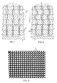
- the new contact probe arrangement consists of a series of stacked perforated plates 1 and 1a, through which the contact probes 2 extend.
- the perforated plates 1a are also referred to as perforated plates of the first type and the perforated plates 1 as such of the second type.
- the perforated plates 1 a which are arranged to be displaceable in the vertical direction, are pressed down in the idle state of the contact probe arrangement by helical compression springs, not shown, arranged between the uppermost perforated plate 1 a and the lowermost perforated plate 1, in the edge region of the perforated plates, so that the lower ends the contact probes 2 are protected by the perforated plates 1a.
- the perforated plates 1 are preferably provided with elongated holes 3, as the top view according to FIG. 3 shows.
- the perforated plates can also be provided with all rectangular, square, circular, elliptical or trapezoidal holes.
- the stacked perforated plates are held together by bolts not shown in Fig. 1.
- the perforated plates 1 are arranged in the plate stack in such a way that of three perforated plates 1 stacked one on top of the other, the middle plate is offset from the other two, in alignment with one another, so that each contact probe 2 is positioned from a part of the bottom hole edge of the top and a part of the top hole edge of the middle , and is enclosed by part of the lower edge of the middle and part of the upper edge of the lower perforated plate. It is thereby achieved that the contact probe can bend under axial load at most up to the part of the hole wall which limits its maximum bending.
- two elongated perforated plates 1 lying one above the other are offset from one another in such a way that the right semicircle of the elongated hole 3 of the upper perforated plate and the left semicircle of the elongated hole 3 of the lower perforated plate overlap. This ensures that the contact probe 2 cannot bend laterally in the plane which is determined by the semicircular lower edge of the upper and the semicircular upper edge of the lower elongated plate 1. You can also not in the plane of contact between the lower and the underlying elongated plate 1, which is aligned with the top.
- each elongated hole is preferably twice the diameter of the contact probes.
- the large side of the rectangular holes, the side length of the square holes, the main axis of the elliptical holes and the height of the trapezoid in the case of trapezoidal holes are twice the diameter of the contact probes.
- the contact probe arrangement is lowered onto the connection surface 4 of the test specimen 5 indicated in FIG. 2. As soon as its lowest perforated plate 1, which is displaceable in the vertical direction, touches the test specimen 5, it is moved upwards against the action of the helical compression spring and the lower ends of the contact probes 2 are released for contacting the connection surfaces 4. Further lowering of the contact probe arrangement with respect to the immovably arranged test specimen 5 ensures the required low contact resistance between the contact probes 2 and the connection surfaces 4 of the test specimen 5 due to the resulting pressure stress on the contact probes 2. When the contact probes 2 are subjected to vertical pressure, they bend as in Fig. 2 shown from the side.
- the lateral bending is greatest in the middle of the height of each perforated plate 1 and, in the case of the use of elongated perforated plates, is limited by the semicircular perforated wall of an elongated hole 3 to such a value that the low contact resistance between the contact probes 2 required for a reliable test result and the connection surfaces 4 of the test specimen 5 is still reliably guaranteed.
- the semicircular perforated wall of an elongated hole 3 to such a value that the low contact resistance between the contact probes 2 required for a reliable test result and the connection surfaces 4 of the test specimen 5 is still reliably guaranteed.
- the contact probe arrangement described offers a number of additional advantages in addition to the possibility of using contact probes of smaller diameter, which was mentioned at the outset.
- the adaptability of the contact probe arrangement to differences in height of the connection surfaces 4 of the test specimen 5 can be increased as desired by increasing the number of perforated plates 1. Due to the stack of perforated plates, larger pressure forces can also be exerted on the contact probes.
- the threading of the contact probes 2 designed as wires through the perforated plate stack is considerably simplified in that the perforated plates 1 are not offset from one another during threading and the entire perforated area is available for threading the contact probes 2. Only then are the perforated plates 1 offset from one another and fixed in this position by the screw bolt.
- the contact probe arrangement according to the invention in contrast to the test device according to the prior art mentioned in the introduction to the description, does not produce any significant forces which run transversely to the axis of the contact probes 2 and which would have to be absorbed by complex mechanical holders.
- the transverse forces which occur are each compensated for within two perforated plates 1, since a contact probe 2, for example, bends to the right in the elongated hole 3 of the upper plate 1 and to the left in the perforated plate below it.
Claims (10)
- Dispositif à sondes de contact pour raccorder électriquement un dispositif d'essai aux surfaces circulaires de raccordement d'un spécimen, et dont on applique les sondes de contact perpendiculairement sur les surfaces de raccordement, pour obtenir une faible résistance de contact, les sondes de contact fléchissant latéralement de manière à s'adapter à des différences de hauteur des surfaces de raccordement, dues à des inégalités de la surface du spécimen,
caractérisé par le fait
que les sondes de contact (2) traversent, au-dessous d'une masse d'enrobage en matière plastique, des plaques perforées empilées (1,1a), utilisées comme plaques de guidage pour les sondes,
que la pile de plaques perforées est constituée de deux types de plaques perforées, dont le premier comprend les plaques perforées (1a) situées au niveau le plus bas et dont les trous sont agencés de manière à garantir une application verticale des sondes de contact (2) sur les surfaces de raccordement (4) du spécimen (5),
que parmi respectivement trois plaques perforées empilées (1) du second type, la plaque médiane est décalée par rapport aux deux autres plaques, alignées entre elles, de manière que chaque sonde de contact (2) est entourée par une partie du bord inférieur du trou de la plaque perforée supérieure et par une partie du bord supérieur du trou de la plaque médiane perforée ainsi que par une partie du bord inférieur du trou de la plaque médiane perforée et par une partie du bord supérieur du trou de la plaque inférieure perforée, de sorte que, lors de l'application d'une charge axiale, la sonde de contact peut fléchir au maximum jusqu'à la partie de la paroi du trou, qui limite son fléchissement maximum. - Dispositif à sondes de contact selon la revendication 1, caractérisé en ce
que toutes les plaques perforées d'un type sont identiques. - Dispositif à sondes de contact selon la revendication 1, caractérisé en ce
que les plaques perforées du premier type possèdent des trous circulaires ou des trous carrés, et
que le diamètre des trous circulaires ou la longueur des côtés des trous carrés est seulement légèrement supérieure au diamètre des sondes de contact. - Dispositif à sondes de contact selon la revendication 1, caractérisé en ce
que les plaques perforées du second type comportent des trous allongés ou des trous rectangulaires ou carrés ou circulaires ou elliptiques ou trapézoïdaux. - Dispositif à sondes de contact selon la revendication 1, caractérisé en ce
que la plaque inférieure ou la plaque supérieure de deux plaques perforées du second type, superposées, comportant des trous allongés ou des trous rectangulaires carrés ou circulaires ou elliptiques ou trapézoïdaux, est identique à l'une des plaques supérieure ou inférieure, mais est pivotée de 180° par rapport à cette plaque. - Dispositif à sondes de contact selon la revendication 1, caractérisé en ce
que les axes longitudinaux des trous allongés ou les grands côtés des trous rectangulaires ou les grands axes des trous elliptiques ou les axes de symétrie des trous trapézoïdaux des plaques perforées du second type sont inclinés de 45° ou de 135° par rapport à l'axe X. - Dispositif à sondes de contact selon la revendication 1, caractérisé en ce
que, dans le cas des plaques perforées du second type, les axes longitudinaux des trous allongés ou les grands côtés des trous rectangulaires ou les longueurs des côtés des trous carrés ou le diamètre des trous circulaires ou le grand axe des trous elliptiques ou la hauteur du trapèze des trous trapézoïdaux sont au moins égaux au double du diamètre des sondes de contact. - Dispositif à sondes de contact selon la revendication 1, caractérisé en ce
que chaque plaque perforée est formée par la réunion de plusieurs plaques perforées partielles. - Dispositif à sondes de contact selon la revendication 1, caractérisé en ce
que les plaques perforées du premier type peuvent être déplacées dans une direction perpendiculaire. - Dispositif à sondes de contact selon la revendication 1, caractérisé en ce
que l'épaisseur des plaques perforées est égale à 2 mm.
Priority Applications (4)
| Application Number | Priority Date | Filing Date | Title |
|---|---|---|---|
| DE8787104577T DE3773904D1 (de) | 1987-03-27 | 1987-03-27 | Kontaktsonden-anordnung zur elektrischen verbindung einer pruefeinrichtung mit den kreisfoermigen anschlussflaechen eines prueflings. |
| EP87104577A EP0283545B1 (fr) | 1987-03-27 | 1987-03-27 | Arrangement des pointes de contact pour la connexion électrique d'un dispositif d'essai avec la surface circulaire de contact d'un spécimen |
| JP63027814A JPH067153B2 (ja) | 1987-03-27 | 1988-02-10 | 接触プローブ装置 |
| US07/167,676 US4843315A (en) | 1987-03-27 | 1988-03-14 | Contact probe arrangement for electrically connecting a test system to the contact pads of a device to be tested |
Applications Claiming Priority (1)
| Application Number | Priority Date | Filing Date | Title |
|---|---|---|---|
| EP87104577A EP0283545B1 (fr) | 1987-03-27 | 1987-03-27 | Arrangement des pointes de contact pour la connexion électrique d'un dispositif d'essai avec la surface circulaire de contact d'un spécimen |
Publications (2)
| Publication Number | Publication Date |
|---|---|
| EP0283545A1 EP0283545A1 (fr) | 1988-09-28 |
| EP0283545B1 true EP0283545B1 (fr) | 1991-10-16 |
Family
ID=8196877
Family Applications (1)
| Application Number | Title | Priority Date | Filing Date |
|---|---|---|---|
| EP87104577A Expired - Lifetime EP0283545B1 (fr) | 1987-03-27 | 1987-03-27 | Arrangement des pointes de contact pour la connexion électrique d'un dispositif d'essai avec la surface circulaire de contact d'un spécimen |
Country Status (4)
| Country | Link |
|---|---|
| US (1) | US4843315A (fr) |
| EP (1) | EP0283545B1 (fr) |
| JP (1) | JPH067153B2 (fr) |
| DE (1) | DE3773904D1 (fr) |
Cited By (1)
| Publication number | Priority date | Publication date | Assignee | Title |
|---|---|---|---|---|
| DE19627442A1 (de) * | 1996-07-08 | 1998-01-22 | Ibm | Klebeverbindung für dicht angeordnete Elemente |
Families Citing this family (43)
| Publication number | Priority date | Publication date | Assignee | Title |
|---|---|---|---|---|
| DE3886754D1 (de) * | 1988-10-19 | 1994-02-10 | Ibm Deutschland | Vorrichtung zum Plasma- oder reaktiven Ionenätzen und Verfahren zum Ätzen schlecht wärmeleitender Substrate. |
| ATE140542T1 (de) * | 1991-04-11 | 1996-08-15 | Methode Electronics Inc | Gerät zum elektronischen testen von gedruckten leiterplatten oder ähnlichem |
| US5225777A (en) * | 1992-02-04 | 1993-07-06 | International Business Machines Corporation | High density probe |
| JPH0677467B2 (ja) * | 1992-12-25 | 1994-09-28 | 山一電機株式会社 | Icソケット |
| US5367254A (en) * | 1993-02-01 | 1994-11-22 | International Business Machines Corporation | Test probe assembly using buckling wire probes within tubes having opposed overlapping slots |
| US5657394A (en) * | 1993-06-04 | 1997-08-12 | Integrated Technology Corporation | Integrated circuit probe card inspection system |
| DE69326609T2 (de) * | 1993-07-23 | 2000-04-27 | Ibm | Testsondenanordnung mit Knicknadeln |
| DE4406538A1 (de) | 1994-02-28 | 1995-08-31 | Mania Gmbh | Leiterplatten-Prüfeinrichtung mit Prüfadapter und Verfahren zum Einstellen desselben |
| EP0685742B1 (fr) | 1994-06-01 | 2001-01-03 | International Business Machines Corporation | Elément de contact coaxial et de transmission de signaux à haute vitesse |
| JPH0837212A (ja) * | 1994-07-22 | 1996-02-06 | Tokyo Electron Ltd | プローブヘッドおよびそれを用いた検査方法 |
| US5597317A (en) * | 1995-08-11 | 1997-01-28 | W. L. Gore & Associates, Inc. | Surface mating electrical connector |
| DE19538792C2 (de) * | 1995-10-18 | 2000-08-03 | Ibm | Kontaktsonden-Anordnung zum elektrischen Verbinden einer Prüfeinrichtung mit den kreisförmigen Anschlußflächen eines Prüflings |
| DE19625493C1 (de) * | 1996-06-26 | 1997-11-20 | Ibm | Kontaktsonden-Anordnung für den elektronischen Funktionstest |
| US5759048A (en) * | 1996-12-11 | 1998-06-02 | The Whitaker Corporation | Board to board connector |
| US5923178A (en) * | 1997-04-17 | 1999-07-13 | Cerprobe Corporation | Probe assembly and method for switchable multi-DUT testing of integrated circuit wafers |
| ATE260470T1 (de) * | 1997-11-05 | 2004-03-15 | Feinmetall Gmbh | Prüfkopf für mikrostrukturen mit schnittstelle |
| DE59810893D1 (de) | 1997-11-05 | 2004-04-08 | Feinmetall Gmbh | Prüfkopf für Mikrostrukturen mit Schnittstelle |
| US6411112B1 (en) | 1998-02-19 | 2002-06-25 | International Business Machines Corporation | Off-axis contact tip and dense packing design for a fine pitch probe |
| DE19811795C1 (de) * | 1998-03-18 | 1999-09-02 | Atg Test Systems Gmbh | Nadel für einen Prüfadapter |
| US6024579A (en) * | 1998-05-29 | 2000-02-15 | The Whitaker Corporation | Electrical connector having buckling beam contacts |
| US6429672B2 (en) | 1998-06-30 | 2002-08-06 | International Business Machines Corporation | Contamination-tolerant electrical test probe |
| DE19844428B4 (de) | 1998-09-28 | 2004-05-13 | Atg Test Systems Gmbh & Co.Kg | Prüfsonde für einen Fingertester, ein Verfahren zum Ansteuern einer Prüfsonde, Fingertester zum Prüfen von Leiterplatten und ein Verfahren zum Prüfen von Leiterplatten mit einem Fingertester |
| US6404211B2 (en) | 1999-02-11 | 2002-06-11 | International Business Machines Corporation | Metal buckling beam probe |
| US6426637B1 (en) | 1999-12-21 | 2002-07-30 | Cerprobe Corporation | Alignment guide and signal transmission apparatus and method for spring contact probe needles |
| FR2815127B1 (fr) * | 2000-10-05 | 2002-12-20 | Andre Sabatier | Connecteur electrique a contacts multiples |
| DE10057457A1 (de) * | 2000-11-20 | 2002-05-23 | Test Plus Electronic Gmbh | Testadapter zum Testen einer Leiterplatine |
| US6530511B2 (en) * | 2001-02-13 | 2003-03-11 | Medallion Technology, Llc | Wire feed mechanism and method used for fabricating electrical connectors |
| US6729026B2 (en) | 2001-02-13 | 2004-05-04 | Medallion Technology, Llc | Rotational grip twist machine and method for fabricating bulges of twisted wire electrical connectors |
| US6528759B2 (en) | 2001-02-13 | 2003-03-04 | Medallion Technology, Llc | Pneumatic inductor and method of electrical connector delivery and organization |
| US6584677B2 (en) | 2001-02-13 | 2003-07-01 | Medallion Technology, Llc | High-speed, high-capacity twist pin connector fabricating machine and method |
| US6447328B1 (en) * | 2001-03-13 | 2002-09-10 | 3M Innovative Properties Company | Method and apparatus for retaining a spring probe |
| JP4365066B2 (ja) * | 2002-04-11 | 2009-11-18 | 株式会社エンプラス | 電気部品用ソケット |
| US6716038B2 (en) | 2002-07-31 | 2004-04-06 | Medallion Technology, Llc | Z-axis connection of multiple substrates by partial insertion of bulges of a pin |
| JP2004085261A (ja) * | 2002-08-23 | 2004-03-18 | Tokyo Electron Ltd | プローブピン及びコンタクタ |
| JP2004342466A (ja) | 2003-05-15 | 2004-12-02 | Yamaichi Electronics Co Ltd | 半導体装置用ソケットの組立方法 |
| JP4636865B2 (ja) * | 2004-12-13 | 2011-02-23 | 井上商事株式会社 | プリント配線板の検査治具 |
| FR2889889B1 (fr) * | 2005-08-22 | 2009-03-20 | Andre Sabatier | Connecteur electrique intercalaire du type a aiguilles |
| EP1959521A1 (fr) * | 2007-02-13 | 2008-08-20 | André Sabatier | Connecteur électrique intercalaire du type à aiguilles |
| WO2009016746A1 (fr) * | 2007-08-01 | 2009-02-05 | Elia Co., Ltd. | Contacteur et ensemble d'interface |
| US8613622B2 (en) | 2011-02-15 | 2013-12-24 | Medallion Technology, Llc | Interconnection interface using twist pins for testing and docking |
| US8994393B2 (en) | 2012-09-06 | 2015-03-31 | International Business Machines Corporation | High-frequency cobra probe |
| JP6484137B2 (ja) * | 2014-11-26 | 2019-03-13 | 株式会社日本マイクロニクス | プローブ及び接触検査装置 |
| JP6872960B2 (ja) * | 2017-04-21 | 2021-05-19 | 株式会社日本マイクロニクス | 電気的接続装置 |
Family Cites Families (8)
| Publication number | Priority date | Publication date | Assignee | Title |
|---|---|---|---|---|
| DE68270C (de) * | Firma GEBRÜDER BONTMY in Paris: | Drehsetzmaschine | ||
| US3904934A (en) * | 1973-03-26 | 1975-09-09 | Massachusetts Inst Technology | Interconnection of planar electronic structures |
| US3941442A (en) * | 1973-10-09 | 1976-03-02 | E. I. Du Pont De Nemours And Company | Daughter board contact |
| US4027935A (en) * | 1976-06-21 | 1977-06-07 | International Business Machines Corporation | Contact for an electrical contactor assembly |
| DE3123627A1 (de) * | 1981-06-15 | 1982-12-30 | Siemens AG, 1000 Berlin und 8000 München | Vorrichtung zum gleichzeitigen kontaktieren mehrerer eng beisammenliegender pruefpunkte, insbesondere von rasterfeldern |
| DE3337915A1 (de) * | 1982-10-21 | 1984-05-24 | Feinmetall Gmbh, 7033 Herrenberg | Kontaktiervorrichtung |
| US4622514A (en) * | 1984-06-15 | 1986-11-11 | Ibm | Multiple mode buckling beam probe assembly |
| DE3473651D1 (en) * | 1984-06-22 | 1988-09-29 | Ibm Deutschland | Buckling beam test probe assembly |
-
1987
- 1987-03-27 DE DE8787104577T patent/DE3773904D1/de not_active Expired - Lifetime
- 1987-03-27 EP EP87104577A patent/EP0283545B1/fr not_active Expired - Lifetime
-
1988
- 1988-02-10 JP JP63027814A patent/JPH067153B2/ja not_active Expired - Lifetime
- 1988-03-14 US US07/167,676 patent/US4843315A/en not_active Expired - Fee Related
Cited By (1)
| Publication number | Priority date | Publication date | Assignee | Title |
|---|---|---|---|---|
| DE19627442A1 (de) * | 1996-07-08 | 1998-01-22 | Ibm | Klebeverbindung für dicht angeordnete Elemente |
Also Published As
| Publication number | Publication date |
|---|---|
| JPH067153B2 (ja) | 1994-01-26 |
| JPS63255671A (ja) | 1988-10-21 |
| EP0283545A1 (fr) | 1988-09-28 |
| DE3773904D1 (de) | 1991-11-21 |
| US4843315A (en) | 1989-06-27 |
Similar Documents
| Publication | Publication Date | Title |
|---|---|---|
| EP0283545B1 (fr) | Arrangement des pointes de contact pour la connexion électrique d'un dispositif d'essai avec la surface circulaire de contact d'un spécimen | |
| DE69831629T2 (de) | Gitteranordnung der Elektroden auf einer Mehrlagenleiterplatte | |
| DE60114200T2 (de) | Keramischer vielschichtkondensatornetzwerk | |
| DE2364786C2 (de) | Elektromechanische Tastsonde mit parallelen Kontaktnadeln | |
| EP2210115B1 (fr) | Cassette à grille pleine surface pour un testeur parallèle servant à tester un circuit imprimé nu, pointe de contact à ressort pour une telle cassette à grille pleine surface et adaptateur pour un testeur parallèle servant à tester un circuit imprimé nu | |
| EP1497862B1 (fr) | Composant a semi-conducteurs comportant une structure capacitive integree en forme de grille | |
| DE10046910A1 (de) | Halbleitervorrichtung | |
| EP0142119B1 (fr) | Dispositif pour adapter le pas d'une grille de contact d'un appareil de contrôle de circuits imprimés | |
| DE10065703A1 (de) | Säulentransistor in einer Halbleitervorrichtung | |
| EP0513715A1 (fr) | Arrangement de lignes conductrices pour circuits à haute intégration | |
| WO2001006562A1 (fr) | Ensemble de boitiers a puce memoire du type boitier mince a connexions courtes (tsop) | |
| EP0268969B1 (fr) | Adaptateur pour un dispositif d'essai de cartes imprimées | |
| DE102007039728A1 (de) | Tastkopfanordnung | |
| CH617487A5 (fr) | ||
| EP0145830A1 (fr) | Rangée de lames de contact pour un dispositif de test pour circuits imprimés contrôlé par un processeur | |
| DE10234945B3 (de) | Halbleiterspeicher mit einer Anordnung von Speicherzellen | |
| DE602004009662T2 (de) | Kontaktstift für einen Prüfkopf | |
| EP0184619B1 (fr) | Dispositif de test pour circuits imprimés | |
| DE102005002678A1 (de) | Ritzrahmen mit verbesserter Füllroutine | |
| DE19724222A1 (de) | DRAM und Verfahren zum Herstellen desselben | |
| DE102009035926B4 (de) | Kompakte Speicherarrays | |
| DE10132668B4 (de) | Halbleitervorrichtung mit definierter Eingangs- /Ausgangsblockgröße und Verfahren zu deren Entwicklung | |
| EP0938749A1 (fr) | Circuit integre muni d'un boitier le contenant | |
| EP0068493B1 (fr) | Assemblage de sondes d'essai pour circuits intégrés | |
| DE10252819A1 (de) | Halbleitermodul |
Legal Events
| Date | Code | Title | Description |
|---|---|---|---|
| PUAI | Public reference made under article 153(3) epc to a published international application that has entered the european phase |
Free format text: ORIGINAL CODE: 0009012 |
|
| AK | Designated contracting states |
Kind code of ref document: A1 Designated state(s): DE FR GB IT |
|
| 17P | Request for examination filed |
Effective date: 19890117 |
|
| 17Q | First examination report despatched |
Effective date: 19901217 |
|
| GRAA | (expected) grant |
Free format text: ORIGINAL CODE: 0009210 |
|
| AK | Designated contracting states |
Kind code of ref document: B1 Designated state(s): DE FR GB IT |
|
| REF | Corresponds to: |
Ref document number: 3773904 Country of ref document: DE Date of ref document: 19911121 |
|
| GBT | Gb: translation of ep patent filed (gb section 77(6)(a)/1977) | ||
| ITF | It: translation for a ep patent filed |
Owner name: IBM - DR. ARRABITO MICHELANGELO |
|
| ET | Fr: translation filed | ||
| PLBE | No opposition filed within time limit |
Free format text: ORIGINAL CODE: 0009261 |
|
| STAA | Information on the status of an ep patent application or granted ep patent |
Free format text: STATUS: NO OPPOSITION FILED WITHIN TIME LIMIT |
|
| 26N | No opposition filed | ||
| PGFP | Annual fee paid to national office [announced via postgrant information from national office to epo] |
Ref country code: GB Payment date: 19930216 Year of fee payment: 7 |
|
| PGFP | Annual fee paid to national office [announced via postgrant information from national office to epo] |
Ref country code: FR Payment date: 19930226 Year of fee payment: 7 |
|
| PG25 | Lapsed in a contracting state [announced via postgrant information from national office to epo] |
Ref country code: GB Effective date: 19940327 |
|
| GBPC | Gb: european patent ceased through non-payment of renewal fee |
Effective date: 19940327 |
|
| PG25 | Lapsed in a contracting state [announced via postgrant information from national office to epo] |
Ref country code: FR Effective date: 19941130 |
|
| REG | Reference to a national code |
Ref country code: FR Ref legal event code: ST |
|
| PGFP | Annual fee paid to national office [announced via postgrant information from national office to epo] |
Ref country code: DE Payment date: 19991223 Year of fee payment: 14 |
|
| PG25 | Lapsed in a contracting state [announced via postgrant information from national office to epo] |
Ref country code: DE Free format text: LAPSE BECAUSE OF NON-PAYMENT OF DUE FEES Effective date: 20020101 |
|
| PG25 | Lapsed in a contracting state [announced via postgrant information from national office to epo] |
Ref country code: IT Free format text: LAPSE BECAUSE OF NON-PAYMENT OF DUE FEES Effective date: 20050327 |