EP0280282A2 - Magnetometer mit Josephson-Element - Google Patents
Magnetometer mit Josephson-Element Download PDFInfo
- Publication number
- EP0280282A2 EP0280282A2 EP88102757A EP88102757A EP0280282A2 EP 0280282 A2 EP0280282 A2 EP 0280282A2 EP 88102757 A EP88102757 A EP 88102757A EP 88102757 A EP88102757 A EP 88102757A EP 0280282 A2 EP0280282 A2 EP 0280282A2
- Authority
- EP
- European Patent Office
- Prior art keywords
- signal
- light
- superconducting
- light signal
- phototransistor
- Prior art date
- Legal status (The legal status is an assumption and is not a legal conclusion. Google has not performed a legal analysis and makes no representation as to the accuracy of the status listed.)
- Granted
Links
- 230000004907 flux Effects 0.000 claims abstract description 36
- 230000000737 periodic effect Effects 0.000 claims abstract description 20
- 230000005540 biological transmission Effects 0.000 claims description 18
- 238000006243 chemical reaction Methods 0.000 claims description 15
- 238000001514 detection method Methods 0.000 claims description 11
- 230000001360 synchronised effect Effects 0.000 claims description 10
- 230000010355 oscillation Effects 0.000 claims description 6
- 238000011896 sensitive detection Methods 0.000 claims description 6
- 230000003321 amplification Effects 0.000 claims description 5
- 238000003199 nucleic acid amplification method Methods 0.000 claims description 5
- 230000003287 optical effect Effects 0.000 claims description 4
- 229910052758 niobium Inorganic materials 0.000 claims description 2
- 239000010955 niobium Substances 0.000 claims description 2
- GUCVJGMIXFAOAE-UHFFFAOYSA-N niobium atom Chemical compound [Nb] GUCVJGMIXFAOAE-UHFFFAOYSA-N 0.000 claims description 2
- 239000002887 superconductor Substances 0.000 claims description 2
- QHGVXILFMXYDRS-UHFFFAOYSA-N pyraclofos Chemical compound C1=C(OP(=O)(OCC)SCCC)C=NN1C1=CC=C(Cl)C=C1 QHGVXILFMXYDRS-UHFFFAOYSA-N 0.000 claims 1
- 241000238366 Cephalopoda Species 0.000 abstract description 11
- 239000013307 optical fiber Substances 0.000 description 15
- 239000004065 semiconductor Substances 0.000 description 8
- 230000008859 change Effects 0.000 description 5
- 230000000694 effects Effects 0.000 description 5
- 230000004044 response Effects 0.000 description 5
- 238000010586 diagram Methods 0.000 description 3
- 229910052734 helium Inorganic materials 0.000 description 3
- 239000001307 helium Substances 0.000 description 3
- SWQJXJOGLNCZEY-UHFFFAOYSA-N helium atom Chemical compound [He] SWQJXJOGLNCZEY-UHFFFAOYSA-N 0.000 description 3
- 239000007788 liquid Substances 0.000 description 3
- 239000000463 material Substances 0.000 description 2
- 238000005259 measurement Methods 0.000 description 2
- 230000008054 signal transmission Effects 0.000 description 2
- 239000004020 conductor Substances 0.000 description 1
- 230000004048 modification Effects 0.000 description 1
- 238000012986 modification Methods 0.000 description 1
- 230000005693 optoelectronics Effects 0.000 description 1
- 230000002093 peripheral effect Effects 0.000 description 1
- 230000001105 regulatory effect Effects 0.000 description 1
- 230000035945 sensitivity Effects 0.000 description 1
Images
Classifications
-
- G—PHYSICS
- G01—MEASURING; TESTING
- G01R—MEASURING ELECTRIC VARIABLES; MEASURING MAGNETIC VARIABLES
- G01R33/00—Arrangements or instruments for measuring magnetic variables
- G01R33/02—Measuring direction or magnitude of magnetic fields or magnetic flux
- G01R33/035—Measuring direction or magnitude of magnetic fields or magnetic flux using superconductive devices
- G01R33/0354—SQUIDS
- G01R33/0356—SQUIDS with flux feedback
-
- Y—GENERAL TAGGING OF NEW TECHNOLOGICAL DEVELOPMENTS; GENERAL TAGGING OF CROSS-SECTIONAL TECHNOLOGIES SPANNING OVER SEVERAL SECTIONS OF THE IPC; TECHNICAL SUBJECTS COVERED BY FORMER USPC CROSS-REFERENCE ART COLLECTIONS [XRACs] AND DIGESTS
- Y10—TECHNICAL SUBJECTS COVERED BY FORMER USPC
- Y10S—TECHNICAL SUBJECTS COVERED BY FORMER USPC CROSS-REFERENCE ART COLLECTIONS [XRACs] AND DIGESTS
- Y10S505/00—Superconductor technology: apparatus, material, process
- Y10S505/825—Apparatus per se, device per se, or process of making or operating same
- Y10S505/842—Measuring and testing
- Y10S505/843—Electrical
- Y10S505/845—Magnetometer
- Y10S505/846—Magnetometer using superconductive quantum interference device, i.e. squid
Definitions
- the present invention relates to a magnetometer, and more particularly to a magnetometer using a Josephson device, which is well suited to the detection of a weak magnetic field.
- magnetometers using Josephson devices are known as superconducting quantum interference device (herein strictlyafter, referred to as SQUID) magnetometers.
- the conventional magnetometers are represented by a DC-SQUID magnetometer and an rf-SQUID magnetometer.
- the DC-SQUID magnetometer is an apparatus wherein a magnetic flux interlinking with a superconducting loop which consists of two Josephson junctions and an inductor is observed in the form of direct current as the change of the maximum superconducting current which flows through the superconducting loop (refer to, for example, U. S. Patent 4,389,612 and U. S. Patent 4,567,438).
- the rf-SQUID magnetometer is an apparatus wherein a magnetic flux interlinking with a superconducting loop which consists of a single Josephson junction and an inductor is observed in the form of alternating current as the change of the maximum superconducting current which flows through the superconducting loop.
- the SQUID forming the key point thereof is a passive device which senses the magnetic flux interlinking with the superconducting loop.
- the SQUID using the Josephson junction is immersed in liquid helium, and the output signal thereof is sent through a connecting cable to a measurement circuit as well as a data processor at the room temperature.
- the SQUID measures a very feeble magnetic flux, and the output signal of the Josephson device is also feeble in itself. Therefore, the signal which is sent from the SQUID to the measurement circuit at the room temperature is a very feeble signal of, for example, about 1 ⁇ V. In consequence, the sensitivities of the conventional SQUID magnetometers have been limited by thermal noise at the room temperature.
- a magnetometer for detecting a weak magnetic field is discussed in "IEEE Trans. on Electron Devices," ED27, No. 10 (1980), pp. 1896 - 1908.
- a voltage signal from a magnetic field detecting device for example, DC-SQUID
- a lock-in amplifier the detection output of which is fed back to the detecting device.
- Magnetometers in each of which, in order to solve such a problem, the magnetic flux detecting device susceptible to noise and the peripheral circuit thereof are connected by photo-isolator means so as to electrically insulate them, are disclosed in the official gazettes of Japanese Patent Applications Laid-open No. 82872/1985, No. 35378/1986 and No. 77772/1986.
- PWM pulse width modulation
- the prior-art magnetometers employ an optical fiber or the like as a feedback circuit and therefore have no problem on the rate of response in that portion. Since, however, electrical elements are respectively connected to an optoelectric converter and an electrooptic converter disposed on both the ends of the optical fiber, there is the problem that the merit of high-speed transfer of the optical fiber is not satisfactorily demonstrated due to the electrical elements.
- the first object of the present invention is to provide a magnetometer using a Josephson device, in which noise otherwise developing in an electrooptic converter and an optoelectric converter is reduced to prevent erroneous operations.
- the second object of the present invention is to provide a magnetometer using a Josephson device, which includes a feedback circuit of high response rate.
- a magnetometer using a Josephson device comprising a sensor coil which detects a signal magnetic flux; a superconducting loop which is magnetically coupled with said sensor coil, to generate a periodic voltage corresponding to the interlinking magnetic flux from said sensor coil, and which is formed of an inductor and at least one Josephson junction; means to amplify the periodic voltage from said superconducting loop; synchronously-detection amplifier means to amplify a predetermined frequency component of the periodic voltage amplified by the firstmentioned amplifier means; first electrooptic conversion means to convert the signal amplified by said synchronouslydetecting amplifier means, into a light signal; first light transmission means to transmit the light signal from said first electrooptic conversion means; a superconducting phototransistor which receives the light signal from said first light transmission means and converts it into an electric signal; and a feedback coil which interlinks a magnetic flux corresponding to the electric signal from said superconducting phototransistor, with said superconduct
- An optoelectric converter constructed of the superconducting means operates in such a manner that the superconducting critical current and the resistance of the device change according to the light input at the cryogenic temperature of 4.2 K in liquid helium. Accordingly, noise to develop in the optoelectric conversion operation becomes only the thermal noise of the device itself and the power distribution resistor at 4.2 K. It is therefore possible to prevent the pulse noise, thermal noise at 300 K and noise from a semiconductor as have developed in the optoelectric converter in the prior art. Moreover, since the function of the magnetometer is not affected by the influences of the noise occurrences, the problem of an erroneous operation is eliminated.
- a magnetometer using a Josephson device comprising a sensor coil which detects a signal magnetic flux; a superconducting loop which is magnetically coupled with said sensor coil, to generate a periodic voltage corresponding to the interlinking magnetic flux from said sensor coil, and which is formed of an inductor and at least one Josephson junction; means to amplify the periodic voltage from said superconducting loop; electrooptic conversion means to convert the periodic voltage amplified by the amplification means, into a light signal; synchronous detection means to subject the light signal, per se from said electrooptic conversion means, to synchronous detection in accordance with a predetermined frequency; second light transmission means to transmit the light signal from said synchronous detection means; a superconducting phototransistor which receives the light signal from said second light transmission means and converts it into an electric signal; and a feedback coil which interlinks a magnetic flux corresponding to the electric signal from said superconducting phototransistor, with said superconducting loop; said sensor coil
- the signal processing of the external circuit is entirely executed with the light signals, noise from the external circuit such as power source noise can be prevented. Furthermore, since the feedback operation is executed with the light signal, the response rate becomes remarkably high.
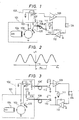
- This embodiment shown in Fig. 1 is such that the feedback circuit of a magnetometer is connected by a photo-isolator, i. e., optical fiber 108.
- a superconducting phototransistor 106 is employed for an optoelectric converter which is disposed at the low temperature part of the photo-isolator in the feedback circuit. Accordingly, noise to develop in the converter can be reduced, and the erroneous operation of the magnetometer can be prevented. More specifically, the optoelectric converter constructed of the superconducting phototransistor operates in such a manner that the superconducting critical current and the resistance of the device change according to a light input at the cryogenic temperature of 4.2 K in liquid helium. Noise to develop on this occasion becomes only the thermal noise of the device and a power distribution resistor at 4.2 K. Therefore, thermal noise at 300 K, noise from a semiconductor held at 300 K, etc. can be prevented, so that the function of the magnetometer is free from any erroneous operation ascribable to the noise.
- a sensor coil 104 for detecting a signal magnetic flux and a DC-SQUID 103 are magnetically coupled.
- the signal magnetic flux interlinking with the sensor coil 104 in a cryogenic atmosphere 101 is input to the DC-SQUID 103.
- This DC-SQUID 103 is biased to a fixed current by a regulated current source.
- thermal noise develops also from the power distribution resistor 123.
- the power distribution resistor 123 is also arranged in the cryogenic atmosphere 101.
- the DC-SQUID 103 biased to the fixed current generates a periodic voltage in correspondence with the interlinking magnetic flux.
- the period of the periodic voltage becomes a quantized magnetic flux ⁇ o (2.07 ⁇ 10 ⁇ 15 Wb).
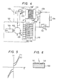
- the relationship between the interlinking magnetic flux and the output voltage of the SQUID is illustrated in Fig. 2.
- the periodic voltage signal is amplified by a battery-driven preamplifier 107, and is delivered to a synchronously-detecting amplifier 109.
- the synchronously-detecting amplifier 109 amplifies the component of the amplified periodic voltage signal at a frequency f .
- the synchronously-detecting amplifier 109 is fed with the signal of the frequency f from an oscillator 111.
- the resulting amplified signal is input to and integrated by an integrator 112.
- An electrooptic converter 110 constructed of a light emitting diode or a semiconductor laser converts the signal from the integrator 112 into light.
- the light signal thus obtained is introduced through the optical fiber 108 into the optoelectric converter constructed of the superconducting phototransistor 106 in the cryogenic atmosphere.
- the superconducting phototransistor 106 has a structure in which a source electrode 131 and a drain electrode 132 made of a superconducting material are disposed on the channel of a semiconductor 133. It is a device the source-drain superconducting critical current and the interelectrode resistance of which are changed by projecting light on the channel.
- Fig. 5 exemplifies the characteristics of the superconducting phototransistor.
- (1) indicates the characteristic without the light projection, and (2) the characteristic with the light projection.
- this device is biased be a proper current, the resistance thereof changes in proportion to the intensity of the projected light, and current to flow therethrough can be controlled.
- the superconducting phototransistor 106 converts the light signal into an electric signal, to apply the feedback current to a feedback coil 105 and to interlink a resulting magnetic flux with the DC-SQUID 103.
- the magnetic flux ⁇ x remains at a point a in Fig. 2.
- the sources of noise occurrences are removed from the vicinities of the DC-SQUID 103, and the resistor to act as the source of thermal noise is arranged in the cryogenic atmosphere.
- Fig. 3 shows a modification to the embodiment of Fig. 1, in which the signal transmission from the preamplifier 107 to the synchronously-detecting amplifier 109 is performed with light as in the feedback circuit.
- the output of the preamplifier 107 is converted into light by an electrooptic converter 110 ⁇ constructed of a light emitting diode or a semiconductor laser, and the light is input through an optical fiber 108 ⁇ to an optoelectric converter 113 constructed of a phototransistor.
- An electric signal produced by the optoelectric converter 113 is input to the synchronously-detecting amplifier 109.
- noise from a lead as develops in the case of introducing the output voltage of the DC-SQUID 103 into the synchronously-detecting amplifier 109 by the use of the lead can be eliminated, to bring forth the effect that noise can be more reduced to prevent erroneous operations.
- an electric signal to be converted from an integrator 112 or a preamplifier 107 is converted by an electrooptic converter 110 or 110 ⁇ into digital light signals, which are transmitted to superconducting phototransistors 106 or an optoelectric converter 113 through optical fibers 108 or 108 ⁇ .
- the digital signals are transmitted in parallel. In this case, there are the effects that the transmission at high speed is possible and that the dynamic range is wide. It is similarly allowed to employ digital signal transmission in a serial scheme which uses only one optical fiber 108 or 108 ⁇ .
- the superconducting phototransistor 106 constitutes the optoelectric converter for generating a feedback current, there is the effect that noise occurs little and that erroneous operations can be prevented.
- connection line of the DC-SQUID 103 with the feedback circuit is made up of the optical fibers, and hence, there is the effect that the amount of conduction heat into a cryogenic vessel can be made less than in case of employing a conductor wiring material.
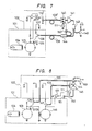
- Fig. 7 shows another embodiment of the present invention.
- the operation of the feedback circuit of a DC-SQUID is executed with light signals.
- the output voltage of the DC-SQUID 103 is amplified by a preamplifier 107, and is thereafter converted into a light signal by a light emitting diode or a semiconductor laser 110 ⁇ .
- This point is the same as in the embodiment of Fig. 3.
- the point of difference of this embodiment from the embodiment of Fig. 3 is that the signal processing of an external circuit is entirely based on light signals. More specifically, the light signal led to the external circuit by an optical fiber 108 ⁇ is input to an optical modulator 140.
- the optical modulator 140 modulates the light signal in accordance with the signal of an oscillation frequency f from an oscillator 111.
- the modulated light signal is amplified by a light amplifier 141.
- This light amplifier 141 is discussed in "1st Opto-Electronic Conference, OEC '86 post deadline papers technical digest, D-11-2 (1986)."
- the light signal amplified by the light amplifier 141 is delivered to a directional photocoupler 143.
- the time constant of the light amplifier 141 is previously set to be sufficiently (one order or more) greater than that of the modulation frequency.
- the light amplifier 141 performs an integral operation. Accordingly, the phase-sensitive detection of the light signal can be carried out with the optical modulator 140 and the light amplifier 141.
- the light signal thus subjected to the phase-sensitive detection and delivered to the direction photocoupler 143 has a part thereof taken out as an output signal by a phototransistor 149. Further, the remaining part of the light signal is input to a directional photocoupler 144.
- the oscillator 111 drives a light emitting diode or semiconductor laser 150 so as to generate a light signal at the oscillation frequency f .
- the directional photocoupler 144 superposes the light signal from the light emitting device 150 and the light signal from the directional photocoupler 143, and the resulting signal is led through an optical fiber 108 to a superconducting phototransistor 106 held in a cryogenic vessel 101.
- the subsequent operation in the cryogenic vessel 101 is the same as in the embodiment of Fig. 3.
- the signal processing in the external circuit is entirely performed with the light signals, so that noise from the external circuit, such as power source noise, can be prevented. Further, the feedback operation is performed with the light signal, so that the response rate can be rendered very high.
- An embodiment in Fig. 8 applies the output signal of a DC-SQUID 103 to an output detecting device 146.
- This output detecting device 146 is constructed of a superconducting quantum interferometer, and it amplifies the above output signal.
- a bias current to be fed to the output detecting device 146 is modulated at a frequency from an oscillator 111 by a superconducting phototransistor 147.
- a superconducting phototransistor 106 is fed with a light signal through an optical fiber 155.
- the output of the output detecting device 146 becomes a train of pulses, which are amplified by a preamplifier 107.
- the output of the DC-SQUID 103 is amplified by the output detecting device 146 constructed of the same superconducting quantum interferometer, the signal-to-noise ratio is enhanced.
- the amplified output of the preamplifier 107 is converted into a light signal by a light emitting device 151 such as light emitting diode or semiconductor laser. Thereafer, the light signal is led out and applied to a light amplifier 145 by an optical fiber 152.
- the light amplifier 145 is fed with a supply voltage from the oscillator 111, and is therefore synchronous with the oscillator 111. For this reason, it operates as the synchronous detector 140 in Fig. 7.
- a part of the output of the light amplifier 145 is diverted by a directional photocoupler 144, and is taken out as an electric signal by a photodetector 153.
- the remaining part of the light signal is led to the superconducting transistor 106 in a cryogenic vessel 101 by the optical fiber 155.
- the superconducting phototransistor 106 converts the led light into an electric signal, and supplies the latter to a feedback coil 105.
- the feedback coil 105 feeds the electric signal of the superconducting phototransistor 106 back to the DC-SQUID 103 as a magnetic flux.
- the feedback operation is carried out as thus far described. In this way, the light signal is directly fed back, so that the response rate becomes remarkably high.
- the crygenic atmosphere and the external circuit are connected by the optical fibers, so that noise such as power source noise can be prevented.
Landscapes
- Physics & Mathematics (AREA)
- Condensed Matter Physics & Semiconductors (AREA)
- General Physics & Mathematics (AREA)
- Measuring Magnetic Variables (AREA)
- Superconductor Devices And Manufacturing Methods Thereof (AREA)
Applications Claiming Priority (2)
| Application Number | Priority Date | Filing Date | Title |
|---|---|---|---|
| JP42552/87 | 1987-02-27 | ||
| JP4255287 | 1987-02-27 |
Publications (3)
| Publication Number | Publication Date |
|---|---|
| EP0280282A2 true EP0280282A2 (de) | 1988-08-31 |
| EP0280282A3 EP0280282A3 (en) | 1990-06-13 |
| EP0280282B1 EP0280282B1 (de) | 1993-07-28 |
Family
ID=12639217
Family Applications (1)
| Application Number | Title | Priority Date | Filing Date |
|---|---|---|---|
| EP88102757A Expired - Lifetime EP0280282B1 (de) | 1987-02-27 | 1988-02-24 | Magnetometer mit Josephson-Element |
Country Status (5)
| Country | Link |
|---|---|
| US (1) | US4906930A (de) |
| EP (1) | EP0280282B1 (de) |
| KR (1) | KR910003449B1 (de) |
| CN (1) | CN1014933B (de) |
| DE (1) | DE3882551T2 (de) |
Cited By (2)
| Publication number | Priority date | Publication date | Assignee | Title |
|---|---|---|---|---|
| DE4139212A1 (de) * | 1990-11-30 | 1992-06-11 | Hitachi Ltd | Mehrkanal-sqid-magnetometer |
| EP0478919A3 (en) * | 1990-10-01 | 1993-07-28 | Dornier Gmbh | Superconducting ad-converter |
Families Citing this family (13)
| Publication number | Priority date | Publication date | Assignee | Title |
|---|---|---|---|---|
| US5442289A (en) * | 1989-07-31 | 1995-08-15 | Biomagnetic Technologies, Inc. | Biomagnetometer having flexible sensor |
| FI95628C (fi) * | 1990-05-15 | 1996-02-26 | Valtion Teknillinen | Menetelmä ja laite pienikohinaisen anturin lähtösignaalin käsittelemiseksi |
| WO1996035972A1 (en) * | 1995-05-08 | 1996-11-14 | Testdesign Corporation | Optical fiber interface for integrated circuit test system |
| US6263189B1 (en) * | 1997-09-29 | 2001-07-17 | The Regents Of The University Of California | Narrowband high temperature superconducting receiver for low frequency radio waves |
| US8747515B2 (en) * | 2003-12-27 | 2014-06-10 | Advance Material Products, Inc | Fully-dense discontinuously-reinforced titanium matrix composites and method for manufacturing the same |
| US7615385B2 (en) | 2006-09-20 | 2009-11-10 | Hypres, Inc | Double-masking technique for increasing fabrication yield in superconducting electronics |
| US7962287B2 (en) * | 2007-07-23 | 2011-06-14 | Schlumberger Technology Corporation | Method and apparatus for optimizing magnetic signals and detecting casing and resistivity |
| CN102483444B (zh) * | 2009-09-09 | 2015-09-30 | 于利希研究中心有限公司 | 具有经由互感感应耦合到squid的线圈的squid |
| US8571614B1 (en) | 2009-10-12 | 2013-10-29 | Hypres, Inc. | Low-power biasing networks for superconducting integrated circuits |
| CN104297703B (zh) * | 2013-07-19 | 2017-03-01 | 中国科学院上海微系统与信息技术研究所 | 超导量子干涉传感器及所适用的磁探测器 |
| CN104345286B (zh) * | 2013-08-06 | 2017-09-01 | 中国科学院上海微系统与信息技术研究所 | 积分电路及所适用的超导量子干涉传感器 |
| US10222416B1 (en) | 2015-04-14 | 2019-03-05 | Hypres, Inc. | System and method for array diagnostics in superconducting integrated circuit |
| US10097281B1 (en) | 2015-11-18 | 2018-10-09 | Hypres, Inc. | System and method for cryogenic optoelectronic data link |
Family Cites Families (13)
| Publication number | Priority date | Publication date | Assignee | Title |
|---|---|---|---|---|
| US3924176A (en) * | 1974-11-11 | 1975-12-02 | Nasa | Magnetometer using superconducting rotating body |
| JPS5577111A (en) * | 1978-12-06 | 1980-06-10 | Toshiba Corp | Superconductive magnet device |
| US4389612A (en) * | 1980-06-17 | 1983-06-21 | S.H.E. Corporation | Apparatus for reducing low frequency noise in dc biased SQUIDS |
| US4489274A (en) * | 1980-12-10 | 1984-12-18 | The United States Of America As Represented By The Secretary Of The Navy | Rotating SQUID magnetometers and gradiometers |
| US4567438A (en) * | 1983-04-04 | 1986-01-28 | Sperry Corporation | SQUID Canister with conical coupling cavity |
| JPS6082872A (ja) * | 1983-10-12 | 1985-05-11 | Yokogawa Hokushin Electric Corp | Squid磁束計 |
| JPS6135378A (ja) * | 1984-07-27 | 1986-02-19 | Yokogawa Hokushin Electric Corp | Squid磁束計 |
| JPS6135574A (ja) * | 1984-07-27 | 1986-02-20 | Hitachi Ltd | 超電導ホトトランジスタ |
| JPS6177772A (ja) * | 1984-09-26 | 1986-04-21 | Yokogawa Hokushin Electric Corp | Squid磁束計 |
| GB2171509B (en) * | 1985-02-23 | 1988-03-09 | Stc Plc | Magnetic field detection |
| US4663590A (en) * | 1985-11-06 | 1987-05-05 | Sperry Corporation | Single frequency noise reduction circuit for squids |
| JP2523517B2 (ja) * | 1986-07-25 | 1996-08-14 | 株式会社日立製作所 | 超電導光検出素子 |
| JP2540511B2 (ja) * | 1986-02-27 | 1996-10-02 | 株式会社日立製作所 | 超電導ホトトランジスタ |
-
1988
- 1988-02-08 US US07/153,047 patent/US4906930A/en not_active Expired - Fee Related
- 1988-02-10 KR KR1019880001259A patent/KR910003449B1/ko not_active Expired
- 1988-02-24 EP EP88102757A patent/EP0280282B1/de not_active Expired - Lifetime
- 1988-02-24 DE DE88102757T patent/DE3882551T2/de not_active Expired - Fee Related
- 1988-02-26 CN CN88101049A patent/CN1014933B/zh not_active Expired
Cited By (3)
| Publication number | Priority date | Publication date | Assignee | Title |
|---|---|---|---|---|
| EP0478919A3 (en) * | 1990-10-01 | 1993-07-28 | Dornier Gmbh | Superconducting ad-converter |
| US5307063A (en) * | 1990-10-01 | 1994-04-26 | Dornier Gmbh | Superconducting A/D converter |
| DE4139212A1 (de) * | 1990-11-30 | 1992-06-11 | Hitachi Ltd | Mehrkanal-sqid-magnetometer |
Also Published As
| Publication number | Publication date |
|---|---|
| DE3882551T2 (de) | 1993-11-18 |
| KR910003449B1 (ko) | 1991-05-31 |
| DE3882551D1 (de) | 1993-09-02 |
| KR880010333A (ko) | 1988-10-08 |
| EP0280282A3 (en) | 1990-06-13 |
| CN1014933B (zh) | 1991-11-27 |
| CN88101049A (zh) | 1988-09-28 |
| US4906930A (en) | 1990-03-06 |
| EP0280282B1 (de) | 1993-07-28 |
Similar Documents
| Publication | Publication Date | Title |
|---|---|---|
| EP0280282B1 (de) | Magnetometer mit Josephson-Element | |
| JP2807518B2 (ja) | 超伝導装置 | |
| EP0205120B1 (de) | Supraleitende Stromfühlerschaltung | |
| JP2662903B2 (ja) | 高感度磁場検出装置 | |
| US5406201A (en) | Magnetic field detecting circuit having a relaxation oscillator SQUID | |
| US6285186B1 (en) | Superconducting quantum interference device having bias wiring layer | |
| EP0501241B1 (de) | Magnetfelddetektionsanordnung mit hoher Empfindlichkeit | |
| JPH01476A (ja) | 磁束計 | |
| JPH01199178A (ja) | 超伝導磁力計 | |
| Podt et al. | Digital squids based on smart dros | |
| EP0829016B1 (de) | Squid magnetometer | |
| JP2673284B2 (ja) | Squid磁束計のキャリブレーション装置 | |
| CA2223767A1 (en) | Voltage step up circuit for magnetometric sensor | |
| JP2929172B2 (ja) | マルチチャンネルsquid磁束計 | |
| KR100403801B1 (ko) | 초전도양자간섭소자 | |
| JPS61281984A (ja) | 磁束計 | |
| JPH04232482A (ja) | Dc−squid磁気検出装置 | |
| JP2613559B2 (ja) | Squid磁束計 | |
| JPH0644034B2 (ja) | 磁束計およびそれに好適な超電導累積演算回路 | |
| JP3013542B2 (ja) | Dc−squid | |
| JPH0740064B2 (ja) | 薄膜squid磁力計 | |
| JPH08220201A (ja) | 超伝導量子干渉計 | |
| JP2609598B2 (ja) | 信号検出方法 | |
| JPH05264697A (ja) | スクイド・コンパレータのバイアス調整回路 | |
| JPH01199179A (ja) | 超伝導磁力計 |
Legal Events
| Date | Code | Title | Description |
|---|---|---|---|
| PUAI | Public reference made under article 153(3) epc to a published international application that has entered the european phase |
Free format text: ORIGINAL CODE: 0009012 |
|
| AK | Designated contracting states |
Kind code of ref document: A2 Designated state(s): DE FR GB |
|
| PUAL | Search report despatched |
Free format text: ORIGINAL CODE: 0009013 |
|
| AK | Designated contracting states |
Kind code of ref document: A3 Designated state(s): DE FR GB |
|
| 17P | Request for examination filed |
Effective date: 19901212 |
|
| 17Q | First examination report despatched |
Effective date: 19920803 |
|
| GRAA | (expected) grant |
Free format text: ORIGINAL CODE: 0009210 |
|
| AK | Designated contracting states |
Kind code of ref document: B1 Designated state(s): DE FR GB |
|
| REF | Corresponds to: |
Ref document number: 3882551 Country of ref document: DE Date of ref document: 19930902 |
|
| ET | Fr: translation filed | ||
| PGFP | Annual fee paid to national office [announced via postgrant information from national office to epo] |
Ref country code: GB Payment date: 19940214 Year of fee payment: 7 |
|
| PGFP | Annual fee paid to national office [announced via postgrant information from national office to epo] |
Ref country code: FR Payment date: 19940217 Year of fee payment: 7 |
|
| PGFP | Annual fee paid to national office [announced via postgrant information from national office to epo] |
Ref country code: DE Payment date: 19940427 Year of fee payment: 7 |
|
| PLBE | No opposition filed within time limit |
Free format text: ORIGINAL CODE: 0009261 |
|
| STAA | Information on the status of an ep patent application or granted ep patent |
Free format text: STATUS: NO OPPOSITION FILED WITHIN TIME LIMIT |
|
| 26N | No opposition filed | ||
| PG25 | Lapsed in a contracting state [announced via postgrant information from national office to epo] |
Ref country code: GB Effective date: 19950224 |
|
| GBPC | Gb: european patent ceased through non-payment of renewal fee |
Effective date: 19950224 |
|
| PG25 | Lapsed in a contracting state [announced via postgrant information from national office to epo] |
Ref country code: FR Effective date: 19951031 |
|
| PG25 | Lapsed in a contracting state [announced via postgrant information from national office to epo] |
Ref country code: DE Effective date: 19951101 |
|
| REG | Reference to a national code |
Ref country code: FR Ref legal event code: ST |