EP0276571A2 - Verfahren zur Herstellung einer Halbleiteranordnung mit einer vergrabenen Zone - Google Patents
Verfahren zur Herstellung einer Halbleiteranordnung mit einer vergrabenen Zone Download PDFInfo
- Publication number
- EP0276571A2 EP0276571A2 EP87311416A EP87311416A EP0276571A2 EP 0276571 A2 EP0276571 A2 EP 0276571A2 EP 87311416 A EP87311416 A EP 87311416A EP 87311416 A EP87311416 A EP 87311416A EP 0276571 A2 EP0276571 A2 EP 0276571A2
- Authority
- EP
- European Patent Office
- Prior art keywords
- conductivity type
- mask
- region
- forming
- epitaxial layer
- Prior art date
- Legal status (The legal status is an assumption and is not a legal conclusion. Google has not performed a legal analysis and makes no representation as to the accuracy of the status listed.)
- Withdrawn
Links
Images
Classifications
-
- H10W10/031—
-
- H10W10/30—
-
- H10W15/00—
-
- H10W15/01—
Definitions
- This invention relates to a method of manufacturing a semiconductor device.
- this invention relates to a method of manufacturing a bipolar transistor with the object of increased miniaturization.
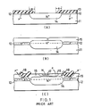
- a P ⁇ diffusion layer 12 is formed on the surface of a P type silicon substrate 11.
- a silicon oxide film 13 of about 0.8 micron thickness is formed on substrate 11, then this is selectively etched away.
- an N+ diffusion layer 14 is formed by injecting antimony (Sb) into substrate 11 by vapour diffusion.
- the thickness of oxide film 13 may be reduced on both sides of the etched region by over-etching. These thin parts of the film allow antimony to pass through, with the result that the region of antimony injection is wider than desired. And since the solid solubility of antimony in silicon is low, to make the collector resistance sufficiently low, a deep N+ diffusion layer 14 must be formed. Thus the extent of this widening in the transverse direction becomes very appreciable.
- an eptiaxial layer 15 is deposited over the whole surface at a temperature of 1100 °C, N type impurities being introduced into it. Whilst this is being done, due to auto-doping, the impurities of P ⁇ diffusion layer 12 and N+ diffusion layer 14 respectively get mixed into N ⁇ epitaxial layer 15. As a result, P ⁇ diffusion layer 12 and N+ diffusion layer 14 respectively extend into epitaxial layer 15, reducing the thickness of epitaxial layer 15.
- the thickness of epitaxial layer 15 may be increased, but if the thickness of epitaxial layer 15 is increased, the thickness of the element separation region must also be increased to a corresponding degree. Consequently, either a ditch-like field insulating film 18 must be formed as shown in Fig. 1(C), or a P type region must be formed over the whole of the thickness of epitaxial layer 15.
- Forming a ditch-like field insulating film 18 makes the manufacturing process complicated. And to form a P type region over the whole of the thickness of epitaxial layer 15, P type impurity must be diffused from above and below epitaxial layer 15 by injecting P type impurity before and after forming epitaxial layer 15. However, if the concentration of P type impurity is made sufficiently high to obtain sufficient mixing of the P type impurity from the layer below epitaxial layer 15, this tends to result in a deterioration of the break-down withstand voltage of the PN junction between substrate 11 and collector region (epitaxial layer 15 and N+ layer 14). The concentration of P type impurity injected from the layer above epitaxial layer 15 cannot be made very high, since it would affect the field inversion voltage.
- An object of this invention is to provide a method of manufacturing a semiconductor device which makes it possible to reduce the element size, yet enable the element to be manufactured with high reliability while using a simple manufacturing process.
- This invention provides a method of manufacturing a semiconductor device comprising, forming an oxidation-resistant film on a semiconductor substrate, forming a mask for etching by providing resist onto the oxidation-resistant film, selectively removing the oxidation-resistant film by isotropic etching using mask, forming a semiconductor region of a first conductivity type on the substrate surface, by introducing impurity of first conductivity type into the semiconductor substrate using the mask, forming an oxide film on the semiconductor substrate by oxidizing the semiconductor substrate using the oxidation-resistant film as a mask, forming a semiconductor region of second conductivity type separated from the semiconductor region of first conductivity type by introducing impurity of second conductivity type into the semiconductor substrate using the oxide film as a mask, and growing an epitaxial layer on the semiconductor substrate.
- the semiconductor region of first conductivity type which has a higher degree of doping than the substrate, and the semiconductor region of second conductivity type can be formed separated from each other in a self-aligned manner.
- the width of the semiconductor region of second conductivity type can be effectively reduced.
- an element isolating region can be formed which maintains sufficient breakdown voltage of the PN junction between the substrate and semiconductor region of second conductivity type.
- arsenic is used as the impurity of the second conductivity type, the width of the second conductivity type semiconductor region can be further reduced.
- the epitaxial layer by growing the epitaxial layer at a low temperature, below 950°C, auto-doping of second conductivity type impurity into this epitaxial layer can be suppressed, making formation of a thick epitaxial layer unnecessary. Also, since the first conductivity type semiconductor region is formed with a high degree of doping, even though the epitaxial layer is grown at low temperature, a sufficient amount of admixture of first conductivity type impurity into this epitaxial layer can be obtained. This therefore facilitates formation of an element isolating region.
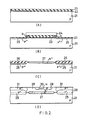
- a thermal oxide film 22 of thickness about 500 to 2000 Angstrom (500 to 2000x10 ⁇ 10m) is formed on the principal surface of a P type (100) silicon substrate 21 of resistivity 0.5 to 20 ohm-cm by heat treatment at 900 to 1000 °C.
- a silicon nitride film 23 is deposited on the thermal oxide film 22, by a CVD method, to a thickness of about 1000 to 5000 Angstrom (1 to 5 x 10 ⁇ 7m).
- silicon film 23 is selectivety etched away by isotropic etching such as CDE etching.
- isotropic etching such as CDE etching.
- that part of the silicon nitride film 23 which is below resist layer 24 is also over-etched, with the result that conversion differences "b" of about 0.25 micron are respectively introduced on both sides thereof.
- resist layer 24 as a mask, boron ions are implanted in substrate 21 to form a P+ impurity region 25.
- resist layer 24 is removed then, using as a mask the silicon nitride film 23 which is left behind, a thermal oxide film 26 of about 0.1 to 1.0 micron thickness is formed in a wet oxidizing atmosphere of 950 to 1000°C. Then, using this thermal oxide film 26 as a mask, N type impurity ions are implanted to form an N+ impurity region 27. In this case, due to the conversion difference b which is introduced in selectively etching the silicon nitride film 23, N+ impurity region 27 is formed separated from P+ impurity region 25.
- N+ impurity region 27 in self-aligned manner in a condition separated from P+ impurity region 25, N+ impurity region 27 can be reduced in size, and the PN junction breakdown voltage between substrate 21 and N+ impurity region 27 can be increased.
- the N type impurity used is arsenic, for example.
- Arsenic has a higher solid solubility in silicon than does antimony, so even though N+ impurity region 27 is made thin, the collector resistance can be lowered to a sufficient degree. Consequently, spreading in the transverse direction of N+ impurity region 27 can be restrained.
- thermal oxide film 26 is removed in NH4F solution, then an N-epitaxial layer 28 is deposited over the entire surface at low temperature i.e. below 950 °C (for example about 800 to 950°C).
- a P type base region 29, N type emitter region 30, and P ⁇ impurity region 31 are then formed.
- P+ impurity region 25 is formed with a high degree of doping, even though N ⁇ epitaxial layer 28 is formed at low temperature, the amount of P type impurities that become admixed with this layer 28 can be made sufficiently large, and (as described above) because the epitaxial layer 28 can be made thin, in forming P ⁇ impurity region 31, only a small amount of impurity is needed to achieve the required object.
- formation of the element isolation region is facilitated.
- the thickness of epitaxial layer 28 formed on the surface of P+ impurity region 25 is thinner than that of epitaxial layer 28 formed on the surface of the N+ impurity region 27. This results in the formation of a step. If this step is utilized as a reference for mask alignment in forming field isolation region, P type base region 29, N type emitter region 30, and P-impurity region 31, misalignment can be reduced.
- P+ impurity region 25 is formed using resist layer 24 as a mask and N+ impurity region 27 is formed using thermal oxide film 26 as a mask.
- N+ impurity region can be formed using the resist layer as a mask and P+ impurity region can be formed using thermal oxide film 26 as a mask.
- this invention provides a method of manufacturing a semiconductor device wherein improvement is achieved in respect of point (i), namely, that with the conventional method of manufacture the width of the buried layer cannot be reduced to lower the collector resistance, so that it is difficult to reduce the element size, and point (ii), namely that if the epitaxial layer is made sufficiently thick to avoid punch-through between emitter and collector, formation of an element isolating region is difficult.
- point (i) namely, that with the conventional method of manufacture the width of the buried layer cannot be reduced to lower the collector resistance, so that it is difficult to reduce the element size
- point (ii) namely that if the epitaxial layer is made sufficiently thick to avoid punch-through between emitter and collector, formation of an element isolating region is difficult.
Landscapes
- Element Separation (AREA)
- Bipolar Transistors (AREA)
Applications Claiming Priority (2)
| Application Number | Priority Date | Filing Date | Title |
|---|---|---|---|
| JP17529/87 | 1987-01-28 | ||
| JP62017529A JPS63185061A (ja) | 1987-01-28 | 1987-01-28 | 半導体装置の製造方法 |
Publications (2)
| Publication Number | Publication Date |
|---|---|
| EP0276571A2 true EP0276571A2 (de) | 1988-08-03 |
| EP0276571A3 EP0276571A3 (de) | 1989-08-02 |
Family
ID=11946450
Family Applications (1)
| Application Number | Title | Priority Date | Filing Date |
|---|---|---|---|
| EP87311416A Withdrawn EP0276571A3 (de) | 1987-01-28 | 1987-12-23 | Verfahren zur Herstellung einer Halbleiteranordnung mit einer vergrabenen Zone |
Country Status (3)
| Country | Link |
|---|---|
| EP (1) | EP0276571A3 (de) |
| JP (1) | JPS63185061A (de) |
| KR (1) | KR920000228B1 (de) |
Cited By (2)
| Publication number | Priority date | Publication date | Assignee | Title |
|---|---|---|---|---|
| EP0525256A1 (de) * | 1991-07-25 | 1993-02-03 | Motorola, Inc. | Verfahren zur Herstellung isolierter Anordnungszonen |
| EP0434182B1 (de) * | 1989-12-22 | 2002-04-03 | Samsung Semiconductor, Inc. | Verfahren zur Herstellung vergrabener Zonen für integrierte Schaltungen |
Family Cites Families (8)
| Publication number | Priority date | Publication date | Assignee | Title |
|---|---|---|---|---|
| JPS57106047A (en) * | 1980-12-23 | 1982-07-01 | Sony Corp | Manufacture of semiconductor integrated circuit device |
| US4381956A (en) * | 1981-04-06 | 1983-05-03 | Motorola, Inc. | Self-aligned buried channel fabrication process |
| JPS59181636A (ja) * | 1983-03-31 | 1984-10-16 | Fujitsu Ltd | 半導体装置 |
| JPS6058637A (ja) * | 1983-09-12 | 1985-04-04 | Nec Corp | 半導体装置の製造方法 |
| US4504330A (en) * | 1983-10-19 | 1985-03-12 | International Business Machines Corporation | Optimum reduced pressure epitaxial growth process to prevent autodoping |
| JPS60124964A (ja) * | 1983-12-12 | 1985-07-04 | Fujitsu Ltd | 半導体装置の製造方法 |
| JPS60154523A (ja) * | 1984-01-24 | 1985-08-14 | Nec Corp | エピタキシヤル層の形成方法 |
| US4583282A (en) * | 1984-09-14 | 1986-04-22 | Motorola, Inc. | Process for self-aligned buried layer, field guard, and isolation |
-
1987
- 1987-01-28 JP JP62017529A patent/JPS63185061A/ja active Pending
- 1987-12-23 EP EP87311416A patent/EP0276571A3/de not_active Withdrawn
- 1987-12-30 KR KR1019870015371A patent/KR920000228B1/ko not_active Expired
Cited By (2)
| Publication number | Priority date | Publication date | Assignee | Title |
|---|---|---|---|---|
| EP0434182B1 (de) * | 1989-12-22 | 2002-04-03 | Samsung Semiconductor, Inc. | Verfahren zur Herstellung vergrabener Zonen für integrierte Schaltungen |
| EP0525256A1 (de) * | 1991-07-25 | 1993-02-03 | Motorola, Inc. | Verfahren zur Herstellung isolierter Anordnungszonen |
Also Published As
| Publication number | Publication date |
|---|---|
| EP0276571A3 (de) | 1989-08-02 |
| KR880009445A (ko) | 1988-09-15 |
| JPS63185061A (ja) | 1988-07-30 |
| KR920000228B1 (ko) | 1992-01-10 |
Similar Documents
| Publication | Publication Date | Title |
|---|---|---|
| EP0701287B1 (de) | Bipolartransistor ohne Leckstrom durch das dünne Basisgebiet und Verfahren zur Herstellung | |
| JPH07118478B2 (ja) | 横方向トランジスタの製造方法 | |
| US5723378A (en) | Fabrication method of semiconductor device using epitaxial growth process | |
| EP0314600B1 (de) | Selbstjustierter Polysiliziumemitter und Kontaktstruktur für Hochleistungsbipolartransistor | |
| JPH05182980A (ja) | ヘテロ接合バイポーラトランジスタ | |
| JP2705344B2 (ja) | 半導体装置及びその製造方法 | |
| EP0221742B1 (de) | Verfahren zur Herstellung von Halbleiterschaltungen um einen bipolaren Transistor mit extrinsischen Basengebieten zu bilden | |
| EP0166923A2 (de) | Hochleistungsbipolartransistor mit einem zwischen dem Emitter und der Extrinsic-Basiszone angeordneten leicht dotierten Schutzring | |
| EP0276571A2 (de) | Verfahren zur Herstellung einer Halbleiteranordnung mit einer vergrabenen Zone | |
| JPS6150390B2 (de) | ||
| JPS5947468B2 (ja) | バイポ−ラ・トランジスタの製造方法 | |
| EP0434182B1 (de) | Verfahren zur Herstellung vergrabener Zonen für integrierte Schaltungen | |
| EP0378164B1 (de) | Bipolarer Transistor und Verfahren zu dessen Herstellung | |
| JP3142336B2 (ja) | 半導体装置及びその製造方法 | |
| EP0042380B1 (de) | Verfahren zum erreichen eines idealen fremdstoffkonzentrationsverlaufs für die basiszone eines transistors | |
| EP0036620B1 (de) | Halbleiterbauelement und Verfahren zu seiner Herstellung | |
| JP2728433B2 (ja) | 半導体装置の製造方法 | |
| JP2532384B2 (ja) | バイポ−ラ・トランジスタとその製法 | |
| JPH04258132A (ja) | 半導体装置およびその製造方法 | |
| KR100216510B1 (ko) | 트렌치를 이용한 바이폴라 트랜지스터의 컬렉터 형성방법 | |
| JPS5984469A (ja) | 半導体装置の製造方法 | |
| KR0147385B1 (ko) | 셀프-어라인 바이폴라 접합 트랜지스터 공정방법 | |
| JPH06333933A (ja) | 半導体装置およびその製造方法 | |
| JP3131986B2 (ja) | バイポーラトランジスタ | |
| JP3083542B2 (ja) | バイポーラ型半導体集積回路装置の製造方法 |
Legal Events
| Date | Code | Title | Description |
|---|---|---|---|
| PUAI | Public reference made under article 153(3) epc to a published international application that has entered the european phase |
Free format text: ORIGINAL CODE: 0009012 |
|
| 17P | Request for examination filed |
Effective date: 19880113 |
|
| AK | Designated contracting states |
Kind code of ref document: A2 Designated state(s): DE FR GB |
|
| PUAL | Search report despatched |
Free format text: ORIGINAL CODE: 0009013 |
|
| AK | Designated contracting states |
Kind code of ref document: A3 Designated state(s): DE FR GB |
|
| 17Q | First examination report despatched |
Effective date: 19911227 |
|
| STAA | Information on the status of an ep patent application or granted ep patent |
Free format text: STATUS: THE APPLICATION IS DEEMED TO BE WITHDRAWN |
|
| 18D | Application deemed to be withdrawn |
Effective date: 19930313 |