EP0243503B1 - Datenaufzeichnungs-wiedergabegerät - Google Patents
Datenaufzeichnungs-wiedergabegerät Download PDFInfo
- Publication number
- EP0243503B1 EP0243503B1 EP86906442A EP86906442A EP0243503B1 EP 0243503 B1 EP0243503 B1 EP 0243503B1 EP 86906442 A EP86906442 A EP 86906442A EP 86906442 A EP86906442 A EP 86906442A EP 0243503 B1 EP0243503 B1 EP 0243503B1
- Authority
- EP
- European Patent Office
- Prior art keywords
- sector
- address
- recording
- alternative
- defective
- Prior art date
- Legal status (The legal status is an assumption and is not a legal conclusion. Google has not performed a legal analysis and makes no representation as to the accuracy of the status listed.)
- Expired
Links
- 230000001172 regenerating effect Effects 0.000 title abstract 3
- 230000002950 deficient Effects 0.000 claims abstract description 76
- 238000001514 detection method Methods 0.000 claims description 12
- 238000000034 method Methods 0.000 description 11
- 238000010586 diagram Methods 0.000 description 8
- 230000003287 optical effect Effects 0.000 description 6
- 230000007547 defect Effects 0.000 description 5
- 239000000463 material Substances 0.000 description 3
- 238000005259 measurement Methods 0.000 description 3
- 230000015572 biosynthetic process Effects 0.000 description 2
- 230000000694 effects Effects 0.000 description 2
- 238000004519 manufacturing process Methods 0.000 description 2
- 235000014676 Phragmites communis Nutrition 0.000 description 1
- 125000004122 cyclic group Chemical group 0.000 description 1
- 230000003247 decreasing effect Effects 0.000 description 1
- 230000008020 evaporation Effects 0.000 description 1
- 238000001704 evaporation Methods 0.000 description 1
- 230000001678 irradiating effect Effects 0.000 description 1
- 230000001788 irregular Effects 0.000 description 1
- 238000007726 management method Methods 0.000 description 1
- 230000001681 protective effect Effects 0.000 description 1
- 238000002310 reflectometry Methods 0.000 description 1
- 239000000758 substrate Substances 0.000 description 1
Images


Classifications
-
- G—PHYSICS
- G11—INFORMATION STORAGE
- G11B—INFORMATION STORAGE BASED ON RELATIVE MOVEMENT BETWEEN RECORD CARRIER AND TRANSDUCER
- G11B20/00—Signal processing not specific to the method of recording or reproducing; Circuits therefor
- G11B20/10—Digital recording or reproducing
- G11B20/18—Error detection or correction; Testing, e.g. of drop-outs
- G11B20/1883—Methods for assignment of alternate areas for defective areas
-
- G—PHYSICS
- G11—INFORMATION STORAGE
- G11B—INFORMATION STORAGE BASED ON RELATIVE MOVEMENT BETWEEN RECORD CARRIER AND TRANSDUCER
- G11B2220/00—Record carriers by type
- G11B2220/20—Disc-shaped record carriers
Definitions
- the present invention relates to an information recording and reproducing apparatus for recording and reproducing information on and from a disk type information recording medium having a plurality of sectors.
- the optical disk is usually provided with a guide track which is detectable optically in order to form tracks with a higher density, and by irradiating a recording layer formed on the guide track with a laser light converted to about 1 pm, a hole is formed or reflectivity is changed to effect the recording of the information.
- the recorded dot and the track pitch are about 1 pm, various defects are caused in a manufacturing process of the optical disk (formation of a guide track, manufacturing of a replica disk, evaporation of a recording material, formation of a protective film, and the like), or depending on an environment in which the disk is used. Due to such defects of the medium, sometimes a defective sector is detected in which a reproduction error occurs in an address or data. Further, in an information recording and reproducing system wherein rewriting is impossible due to the properties of a recording material as isthe case in a write-once type optical disk, if the recording operation is interrupted during data recording, for example, due to a drive error, it results in the recording of incomplete data in a sector, and it is regarded as a defective sector in file management.
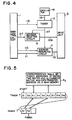
- a defective sector identification method in a pair art information recording and reproducing system is disclosed, for example, in Japanese Patent Application No. 60-49035 (1985). Further, a method for using an alternative sector for a defective sector is disclosed, for example, in Japanese Patent Laid-Open Publication No. 60-75931 (1985). The operation for using alternative sector for a defective sector in the information recording and reproducing system will be described with reference to Fig. 5. For example, it is supposed that defective sectors X1 and X2 exist among sectors S1 to S9 on a track T from which data is intended to be reproduced, and that it is recorded in a register Rg beforehand that alternative sectors are a sector S1' and a sector S2' on a trackT'.
- the defective sector X1 located next to the sector S2 is skipped and the sector S4 is accessed. Further, the defective sector X2 located next to the sector S5 is skipped, and this sector S6 and the sectors following thereto are accessed.
- the track T is sought to successively reproduce from the sectors S1' and S2', and the reproduced data is sent to an area in a main memory to which otherwise reproduced data from the defective sectors X1 and X2 would be sent originally.
- EP-A-0127311 discloses a remapping technique for handling medium defects in a disk drive system.
- a predetermined number of sectors at the end of each cylinder are allocated as spares, the number of spares to which logical addresses are assigned being equal to the number of non-spare sectors which are defective.
- unique patterns instead of logical addresses are assigned.
- the logical addresses are assigned to all non-defective normal sectors and the selected ones of the spare sectors in a sequential manner.
- information recording and reproducing apparatus using a disk-type information recording medium having normal sectors addressed in address areas of respective sector ID fields in a format with an error detecting capability, means for recording information onto said medium and for reproducing information from said medium; and address deleting means, responsive to detection of a defective sector by the error detecting capability, for recording on the address area of said defective sector a delete signal in order to disable the reproduction of the address of said defective sector address area; characterised by said disk-type information recording medium having alternative sectors unrecorded with addresses in the same track with said normal sectors, and said apparatus having address recording means for recording addresses on the address area of any of said alternative sectors, whereby, in response to detecting a defective sector, said address deleting means records the delete signal on the address area of the detected defective sector in order to disable the reproduction thereof, said address recording means records the address of said defective sector on the address area of the unrecorded alternative sector in the same track with said defective sector, and said information recording means records information to be otherwise recorded in said defective sector onto said alternative sector
- Figure 1 is a block diagram of an embodiment of an information recording and reproducing apparatus according to the present invention
- Fig. 2 is an operation outline explaining diagram for explaining an operation for using an alternative sector during data recording
- Fig. 3 is a flowchart for explaining a data recording operation
- Fig. 4 is a block diagram of address deleting means and address recording means which are actuated by using a timer
- Fig. 5 is a operation outline explaining diagram for explaining a prior art operation for using an alternative sector.
- Fig. 1 is a block diagram of an information recording and reproducing apparatus in an embodiment of the present invention.
- reference numeral 1 designates a main control circuit which controls the whole apparatus by receiving a device command from a host system (not shown).
- Reference numeral 2 designates a target sector detecting circuit which performs, after reading ID information such as a track address, a sector address, a CRCC code (cyclic redundancy check code) for error checking, etc., from a reproducing signal 101 delivered from a drive unit 3 and after checking an error with respect to the CRCC, a coincidence detection with a target section address 100 set by the main control circuit 1.
- ID information such as a track address, a sector address, a CRCC code (cyclic redundancy check code) for error checking, etc.
- Reference numeral 5 designates a sector buffer for temporarily storing recording information 104 to be recorded on a target sector and reproduced information 14 reproduced from the target sector.
- Reference numeral 4 designates an information recording circuit which performs digital modulation of (2, 7) RLLC (run length limited code), etc., after coding the recording information 104 by adding thereto an error detection and correction code such as a reed solomon code, and delivers a produced recording signal 105 to a laser driving circuit (not shown) within the drive unit 3.
- Reference numeral 8 designates an information reproducing circuit which takes the reproducing signal 101 delivered from the drive unit 3 into a shift register, and produces the reproduced information 114 after demodulating an output of the shift register by converting in a combining circuit and after decoding the demodulated output.
- Reference numeral 6 designates an address deleting circuit which supplies a delete signal 109 to the drive unit 3, and disables an address from a defective sector to be reproduced by recording the delete signal 109 on an address area in the defective sector by using the laser driving circuit within the drive unit 3.
- Reference numeral 7 designates an address recording circuit which performs digital modulation after adding the CRCC code for error checking to alternative address information 111, delivers the produced alternative address signal 112 to the drive unit 3, and records on the address area of the alternative sector by using the laser driving circuit within the drive unit 3.
- a method for modulating and demodulating the (2, 7) RLLC is disclosed in U.S. Patent No. 4,115,768 issued to Eggenber et al.
- the normal sector S3 is regarded as a defective sector having a defect in the address area.
- the delete signal 109 is overwritten on the address area 13 in the defective sector S3 thereby to make the address of the defective sector S3 completely unable to be reproduced.
- the main control circuit 1 in order to detect a normal sector Sn located precedent to the alternative sector R1, sends and sets the address of the normal sector Sn to the target sector detecting circuit 2 as the target sector address 100.
- the target sector detecting circuit 2 detects the normal sector Sn set by the main control circuit 1
- the target sector detecting circuit 2 delivers the detection signal 103 to the main control circuit 1
- the main control circuit 1 delivers to the address recording circuit 7 the address write enable signal 110 and the alternative address information 111 containing the address of the defective sector S3.
- the drive unit 3 detects the sector mark of the alternative sector R1 and sends the sector mark signal 108, the address recording circuit 7 is actuated, and the address recording circuit 7 produces the alternative address signal 112 from the alternative address information 111 and delivers the alternative address signal 112 to the drive unit 3.
- the drive unit 3 records the alternative address signal 112 on the address area 13 in the alternative sector R1 as shown in Fig. 2, at (C), and by this recording, the same address as the defective sector S3 is recorded on the address area 13 in the alternative sector R1 which has been in an unrecorded condition.
- the disposition of the sectors on the target track is changed as shown in Fig. 2, at (D), and because of the fact that the address of the normal sector S3 is disabled to be reproduced, the normal sector S3 is identified as a defective sector X and also, the alternative sector R1 is identified as an alternative sector S3' which has the same address as the normal sector S3.
- the information which is to be recorded on the normal sector S3 is recorded alternatively on the alternative sector S3', and the operation for the alternative sector is completed.
- the delete signal 109 in the aforementioned procedure (G), when the address area of the information recording medium is formed with an irregular surface structure of the disk substrate as is the case in the write-once type optical disk, or when the rewriting of address information is impossible due to the properties of the recording material, it is possible to disable the address of the defective sector to be reproduced by using as the delete signal 109, for example, a signal having a pulse width wider than the signal contained in the signal 112 of the alternative address, and by overwriting the signal of the wider pulse width on the address area of the defective sector thereby to cause the CRCC error to be generated at the time of reproducing the address.
- the delete signal 109 for example, a signal having a pulse width wider than the signal contained in the signal 112 of the alternative address
- the information recording medium when used in which the rewriting of the address information is possible, it is possible to disable the address of the defective sector to be reproduced, for example, by using as the delete signal 109 a D.C. signal thereby to erase at least a portion of the address area.
- the main control circuit 1 delivers and sets as the target address 100 the address of the normal sector S3 to the target sector detecting circuit 2, and at the same time, delivers the read enable signal 113 to the information reproducing circuit 8.
- the target sector detecting circuit 2 detects address information contained in the reproducing signal 101 and performs coincidence detection with the target sector address 100.
- the target sector detecting circuit 2 detects, in place of the defective sector S3 whose address has been disabled to be reproduced, the alternative sector S3' having the same address recorded therein, the target sector detecting circuit 2 delivers the detection signal 103 to the information reproducing circuit 8.
- the information reproducing circuit 8 produces the reproduced information 114 from the reproducing signal 101 sent from the drive unit 3, and delivery to the sector buffer 5.
- the reproducing circuit 8 finishes the delivery of the reproduced information 114, the reproducing operation is completed when the reproduced information 114 which is stored temporarily in the sector buffer 5 is sent out to the host system.
- the number of the alternative sectors is not limited to this. Further, when a plurality of alternative sectors exist on the same track, the foregoing procedure for alternative sector can be executed also for the alternative sector which is regarded as a defective sector.
- the address deleting circuit 6 and the address recording circuit 7 are actuated by the sector mark signal 108 which is sent out when the drive unit 3 detects the sector mark 11.
- the sector mark 11 is not satisfactory or when the format recording has not been performed, the foregoing operation for alternative sector can not be executed.
- method for actuating the address deleting circuit 6 or the address recording circuit 7 uses a timer for measuring a rotational latency corresponding to one sector in place of the sector mark signal 108. This method will be described with reference to a block diagram in Fig. 4. In Fig.
- the main control circuit 1 delivers measurement data 115 corresponding to a rotational latency corresponding to one sector to actuate a timer 15.
- the timer 15 measures a time corresponding to the measurement data 115 by counting a clock signal 116 delivered from an oscillator 16.
- the timer 15 sends an alternative actuation signal 117 to the address deleting circuit 6 or the address recording circuit 7.
- the address deleting circuit 6 or the address recording circuit 7 is actuated by the alternative actuation signal 117 in place of the sector mark signal 108, and the operation for alternative sector can be executed.
- the information recording and reproducing apparatus in accordance with the present invention, when a defective sector is detected, first, the address of the defective sector is made impossible to be reproduced by recording a delete signal on the address area in the defective sector, then, the address of the defective sector is recorded on the address area in an alternative sector, and further, the information to be recorded on the defective sector is recorded within the alternative sector.
- the alternative sector having the same address and data as the defective sector is formed on the same track as the defective sector. Accordingly, at the time of reproduction, the access to the alternative sector becomes possible without a seek operation, and the processing speed is increased.
- the access to the alternative sector is enabled without using a correspondence table between the defective sector and the alternative sector, the structure of the apparatus can be made simple, and its practical effects are great.
- the information recording and reproducing apparatus uses an information recording medium including on the same track a normal sector having an address formatted on an address area within a sector ID field, and an alternative sector in which an address is not yet recorded.
- the apparatus when a defective sector is detected, first, the address of the defective sector is made impossible to be reproduced by recording a delete signal on the address area in the defective sector, then, the address of the defective sector is recorded on the address area in the alternative sector, and further the information to be recorded on the defective sector is recorded within the alternative sector.
- the alternative sector having the same address and data as the defective sector is formed on the same track as the defective sector. Accordingly, at the time of reproduction, the seek operation for accessing the alternative sector is not needed, and the processing speed is increased.
- the correspondence table between the defective sector and the alternative sector, etc. are not used, there is no need to provide a register and a buffer for administering the correspondence table, and the structure of the apparatus can be made simple.
Landscapes
- Engineering & Computer Science (AREA)
- Signal Processing (AREA)
- Signal Processing For Digital Recording And Reproducing (AREA)
- Optical Recording Or Reproduction (AREA)
Claims (5)
Applications Claiming Priority (2)
| Application Number | Priority Date | Filing Date | Title |
|---|---|---|---|
| JP241060/85 | 1985-10-28 | ||
| JP60241060A JPS62102482A (ja) | 1985-10-28 | 1985-10-28 | 情報記録再生装置 |
Publications (3)
| Publication Number | Publication Date |
|---|---|
| EP0243503A1 EP0243503A1 (de) | 1987-11-04 |
| EP0243503A4 EP0243503A4 (de) | 1988-03-03 |
| EP0243503B1 true EP0243503B1 (de) | 1990-07-18 |
Family
ID=17068707
Family Applications (1)
| Application Number | Title | Priority Date | Filing Date |
|---|---|---|---|
| EP86906442A Expired EP0243503B1 (de) | 1985-10-28 | 1986-10-27 | Datenaufzeichnungs-wiedergabegerät |
Country Status (5)
| Country | Link |
|---|---|
| US (2) | US4885735A (de) |
| EP (1) | EP0243503B1 (de) |
| JP (1) | JPS62102482A (de) |
| DE (1) | DE3672828D1 (de) |
| WO (1) | WO1987002818A1 (de) |
Cited By (6)
| Publication number | Priority date | Publication date | Assignee | Title |
|---|---|---|---|---|
| US5936971A (en) * | 1989-04-13 | 1999-08-10 | Sandisk Corporation | Multi-state flash EEprom system with cache memory |
| US6570790B1 (en) | 1988-06-08 | 2003-05-27 | Sandisk Corporation | Highly compact EPROM and flash EEPROM devices |
| US7447069B1 (en) | 1989-04-13 | 2008-11-04 | Sandisk Corporation | Flash EEprom system |
| US7681057B2 (en) | 2001-09-28 | 2010-03-16 | Lexar Media, Inc. | Power management of non-volatile memory systems |
| US7734862B2 (en) | 2000-07-21 | 2010-06-08 | Lexar Media, Inc. | Block management for mass storage |
| US8166488B2 (en) | 2002-02-22 | 2012-04-24 | Micron Technology, Inc. | Methods of directly accessing a mass storage data device |
Families Citing this family (61)
| Publication number | Priority date | Publication date | Assignee | Title |
|---|---|---|---|---|
| JPH0673226B2 (ja) * | 1987-06-12 | 1994-09-14 | 株式会社シーエスケイ | 光記録媒体の読取誤り検出装置 |
| US5535328A (en) * | 1989-04-13 | 1996-07-09 | Sandisk Corporation | Non-volatile memory system card with flash erasable sectors of EEprom cells including a mechanism for substituting defective cells |
| US7190617B1 (en) | 1989-04-13 | 2007-03-13 | Sandisk Corporation | Flash EEprom system |
| JPH031370A (ja) * | 1989-05-29 | 1991-01-08 | Nec Corp | 磁気デイスク装置の書込み・読出し制御回路 |
| CA2020059C (en) * | 1989-06-30 | 1995-05-23 | Shigemi Maeda | Modular ceramic igniter |
| JP3057498B2 (ja) * | 1989-08-02 | 2000-06-26 | 富士通株式会社 | アレイディスク装置およびそのデータ読み出し方法 |
| JPH03116583A (ja) * | 1989-09-29 | 1991-05-17 | Toshiba Corp | 光ディスク装置 |
| US5737632A (en) * | 1989-12-19 | 1998-04-07 | Hitachi, Ltd. | Magnetic disc control apparatus with parallel data transfer between disc control unit and encoder/decoder circuit |
| JP3373218B2 (ja) * | 1991-12-26 | 2003-02-04 | パイオニア株式会社 | 書込み可能型ディスク用ドライブ装置の記録再生方法 |
| JPH05324489A (ja) * | 1992-05-15 | 1993-12-07 | Toshiba Corp | 記憶装置 |
| JP3225640B2 (ja) * | 1992-10-23 | 2001-11-05 | ソニー株式会社 | 記録装置 |
| US5422761A (en) * | 1992-11-20 | 1995-06-06 | International Business Machines Corporation | Disk drive with redundant recording |
| JPH06314470A (ja) * | 1993-04-30 | 1994-11-08 | Nec Corp | 磁気ディスク装置 |
| EP0640924A3 (de) * | 1993-08-17 | 1997-04-23 | Sony Corp | Vorrichtung zur Wiedergabe von Daten. |
| US5818654A (en) * | 1994-06-13 | 1998-10-06 | Seagate Technology, Inc. | Apparatus and process for managing defective headerless sectors |
| US5983309A (en) * | 1994-07-27 | 1999-11-09 | Seagate Technology, Inc. | Autonomous high speed address translation with defect management for hard disc drives |
| JP3500724B2 (ja) * | 1994-09-05 | 2004-02-23 | ソニー株式会社 | データ再生方法およびデータ再生装置 |
| US5845313A (en) | 1995-07-31 | 1998-12-01 | Lexar | Direct logical block addressing flash memory mass storage architecture |
| US6728851B1 (en) | 1995-07-31 | 2004-04-27 | Lexar Media, Inc. | Increasing the memory performance of flash memory devices by writing sectors simultaneously to multiple flash memory devices |
| US5930815A (en) * | 1995-07-31 | 1999-07-27 | Lexar Media, Inc. | Moving sequential sectors within a block of information in a flash memory mass storage architecture |
| US6801979B1 (en) | 1995-07-31 | 2004-10-05 | Lexar Media, Inc. | Method and apparatus for memory control circuit |
| US6081878A (en) | 1997-03-31 | 2000-06-27 | Lexar Media, Inc. | Increasing the memory performance of flash memory devices by writing sectors simultaneously to multiple flash memory devices |
| US5907856A (en) * | 1995-07-31 | 1999-05-25 | Lexar Media, Inc. | Moving sectors within a block of information in a flash memory mass storage architecture |
| US6978342B1 (en) | 1995-07-31 | 2005-12-20 | Lexar Media, Inc. | Moving sectors within a block of information in a flash memory mass storage architecture |
| US5838614A (en) * | 1995-07-31 | 1998-11-17 | Lexar Microsystems, Inc. | Identification and verification of a sector within a block of mass storage flash memory |
| US6757800B1 (en) | 1995-07-31 | 2004-06-29 | Lexar Media, Inc. | Increasing the memory performance of flash memory devices by writing sectors simultaneously to multiple flash memory devices |
| US8171203B2 (en) | 1995-07-31 | 2012-05-01 | Micron Technology, Inc. | Faster write operations to nonvolatile memory using FSInfo sector manipulation |
| US6125435A (en) * | 1995-09-13 | 2000-09-26 | Lexar Media, Inc. | Alignment of cluster address to block addresses within a semiconductor non-volatile mass storage memory |
| JP3113200B2 (ja) * | 1996-03-25 | 2000-11-27 | 株式会社東芝 | 交替処理方法 |
| JP3029399B2 (ja) * | 1996-03-25 | 2000-04-04 | 株式会社東芝 | 交替処理方法 |
| JP2848809B2 (ja) * | 1996-03-25 | 1999-01-20 | 株式会社東芝 | 交替処理方法 |
| JP3113201B2 (ja) * | 1996-03-25 | 2000-11-27 | 株式会社東芝 | 交替処理方法 |
| JP3029400B2 (ja) * | 1996-03-25 | 2000-04-04 | 株式会社東芝 | 交替処理方法 |
| US5928370A (en) * | 1997-02-05 | 1999-07-27 | Lexar Media, Inc. | Method and apparatus for verifying erasure of memory blocks within a non-volatile memory structure |
| US6034897A (en) * | 1999-04-01 | 2000-03-07 | Lexar Media, Inc. | Space management for managing high capacity nonvolatile memory |
| US6122195A (en) * | 1997-03-31 | 2000-09-19 | Lexar Media, Inc. | Method and apparatus for decreasing block write operation times performed on nonvolatile memory |
| US6411546B1 (en) | 1997-03-31 | 2002-06-25 | Lexar Media, Inc. | Nonvolatile memory using flexible erasing methods and method and system for using same |
| JPH10312650A (ja) * | 1997-05-14 | 1998-11-24 | Ricoh Co Ltd | 光ディスク記録装置 |
| US6076137A (en) | 1997-12-11 | 2000-06-13 | Lexar Media, Inc. | Method and apparatus for storing location identification information within non-volatile memory devices |
| GB9801373D0 (en) | 1998-01-22 | 1998-03-18 | Memory Corp Plc | Memory system |
| JPH11232791A (ja) * | 1998-02-10 | 1999-08-27 | Sony Corp | 情報記録方法及び装置 |
| JP4324276B2 (ja) * | 1998-06-03 | 2009-09-02 | 株式会社日立グローバルストレージテクノロジーズ | 磁気ディスク誤り訂正方法及び装置 |
| US6374337B1 (en) | 1998-11-17 | 2002-04-16 | Lexar Media, Inc. | Data pipelining method and apparatus for memory control circuit |
| ATE340405T1 (de) | 1999-04-01 | 2006-10-15 | Lexar Media Inc | Raumverwaltung in einem nichtflüchtigen speicher mit hoher kapazität |
| US6141249A (en) * | 1999-04-01 | 2000-10-31 | Lexar Media, Inc. | Organization of blocks within a nonvolatile memory unit to effectively decrease sector write operation time |
| US6754680B1 (en) * | 1999-05-20 | 2004-06-22 | Matsushita Electric Industrial Co., Ltd. | Data control equipment, method to control data and recording medium to record data control procedure |
| US6567307B1 (en) | 2000-07-21 | 2003-05-20 | Lexar Media, Inc. | Block management for mass storage |
| GB0123412D0 (en) | 2001-09-28 | 2001-11-21 | Memquest Ltd | Memory system sectors |
| GB0123415D0 (en) | 2001-09-28 | 2001-11-21 | Memquest Ltd | Method of writing data to non-volatile memory |
| GB0123419D0 (en) | 2001-09-28 | 2001-11-21 | Memquest Ltd | Data handling system |
| GB0123416D0 (en) | 2001-09-28 | 2001-11-21 | Memquest Ltd | Non-volatile memory control |
| GB0123410D0 (en) | 2001-09-28 | 2001-11-21 | Memquest Ltd | Memory system for data storage and retrieval |
| GB0123417D0 (en) | 2001-09-28 | 2001-11-21 | Memquest Ltd | Improved data processing |
| US6957295B1 (en) | 2002-01-18 | 2005-10-18 | Lexar Media, Inc. | File management of one-time-programmable nonvolatile memory devices |
| WO2005059854A2 (en) | 2003-12-17 | 2005-06-30 | Lexar Media, Inc. | Electronic equipment point-of-sale activation to avoid theft |
| US7725628B1 (en) | 2004-04-20 | 2010-05-25 | Lexar Media, Inc. | Direct secondary device interface by a host |
| US7370166B1 (en) | 2004-04-30 | 2008-05-06 | Lexar Media, Inc. | Secure portable storage device |
| US7464306B1 (en) | 2004-08-27 | 2008-12-09 | Lexar Media, Inc. | Status of overall health of nonvolatile memory |
| US7594063B1 (en) | 2004-08-27 | 2009-09-22 | Lexar Media, Inc. | Storage capacity status |
| JP2006113833A (ja) * | 2004-10-15 | 2006-04-27 | Hitachi Ltd | ストレージ管理装置、ストレージネットワークシステム、ストレージ管理方法およびプログラム |
| JP5955092B2 (ja) * | 2011-10-12 | 2016-07-20 | パナソニックIpマネジメント株式会社 | 光記録再生装置および再生装置 |
Family Cites Families (17)
| Publication number | Priority date | Publication date | Assignee | Title |
|---|---|---|---|---|
| DE2508706C2 (de) * | 1974-05-02 | 1984-10-11 | International Business Machines Corp., Armonk, N.Y. | Schaltungsanordnung zur Codierung von Datenbitfolgen |
| FR2426938A1 (fr) * | 1978-05-26 | 1979-12-21 | Cii Honeywell Bull | Dispositif de detection de secteurs defectueux et d'allocation de secteurs de remplacement dans une memoire a disques |
| US4259475A (en) * | 1979-03-29 | 1981-03-31 | Exxon Research & Engineering Co. | Preparation of linear crystalline homopolybenzyl |
| JPS5641515A (en) * | 1979-09-12 | 1981-04-18 | Nec Corp | Retry system of magnetic tape memory device |
| JPS5755580A (en) * | 1980-09-20 | 1982-04-02 | Sanyo Electric Co Ltd | Address writing-in method of magnetic disk |
| JPS5832236A (ja) * | 1981-08-18 | 1983-02-25 | Matsushita Electric Ind Co Ltd | 光学的記録再生装置 |
| JPS5835733A (ja) * | 1981-08-26 | 1983-03-02 | Fujitsu Ltd | 情報記録再生方式 |
| JPS58203685A (ja) * | 1982-05-20 | 1983-11-28 | Hitachi Medical Corp | 磁気デイスク制御装置 |
| JPS59113509A (ja) * | 1982-12-20 | 1984-06-30 | Nec Corp | デイスク処理装置 |
| JPS59188814A (ja) * | 1983-04-12 | 1984-10-26 | Nec Corp | 媒体記録方式 |
| EP0127311B1 (de) * | 1983-05-23 | 1990-03-14 | Data General Corporation | Verfahren und Steuereinrichtung zur Behandlung von Fehlern des Aufzeichnungsträgers bei einem Plattenspeichersystem |
| WO1985001380A1 (en) * | 1983-09-19 | 1985-03-28 | Storage Technology Partners Ii | Optical disk format employing resynchronizable data sectors |
| JPS60179980A (ja) * | 1984-02-25 | 1985-09-13 | Canon Inc | 情報記録方法 |
| US4695993A (en) * | 1984-06-15 | 1987-09-22 | Matsushita Electric Industrial Co., Ltd. | Optical information recording and reproducing apparatus and optical disc |
| JPS61208673A (ja) * | 1985-03-12 | 1986-09-17 | Matsushita Electric Ind Co Ltd | 情報記録再生装置 |
| JP2549241B2 (ja) * | 1992-05-22 | 1996-10-30 | インターナショナル・ビジネス・マシーンズ・コーポレイション | コンピュータ・システム |
| JP3199473B2 (ja) * | 1992-08-12 | 2001-08-20 | 株式会社小松製作所 | 抵抗拡散接合方法 |
-
1985
- 1985-10-28 JP JP60241060A patent/JPS62102482A/ja active Pending
-
1986
- 1986-10-27 DE DE8686906442T patent/DE3672828D1/de not_active Expired - Lifetime
- 1986-10-27 WO PCT/JP1986/000539 patent/WO1987002818A1/ja not_active Ceased
- 1986-10-27 EP EP86906442A patent/EP0243503B1/de not_active Expired
- 1986-10-27 US US07/076,170 patent/US4885735A/en not_active Expired - Fee Related
-
1989
- 1989-10-03 US US07/416,834 patent/US4986668A/en not_active Expired - Fee Related
Cited By (17)
| Publication number | Priority date | Publication date | Assignee | Title |
|---|---|---|---|---|
| US6570790B1 (en) | 1988-06-08 | 2003-05-27 | Sandisk Corporation | Highly compact EPROM and flash EEPROM devices |
| US6914817B2 (en) | 1988-06-08 | 2005-07-05 | Sandisk Corporation | Highly compact EPROM and flash EEPROM devices |
| US6914846B2 (en) | 1989-04-13 | 2005-07-05 | Sandisk Corporation | Flash EEprom system |
| US7397713B2 (en) | 1989-04-13 | 2008-07-08 | Sandisk Corporation | Flash EEprom system |
| US6684345B2 (en) | 1989-04-13 | 2004-01-27 | Sandisk Corporation | Flash EEprom system |
| US6757842B2 (en) | 1989-04-13 | 2004-06-29 | Sandisk Corporation | Flash EEprom system |
| US6763480B2 (en) | 1989-04-13 | 2004-07-13 | Sandisk Corporation | Flash EEprom system |
| US6149316A (en) | 1989-04-13 | 2000-11-21 | Sandisk Corporation | Flash EEprom system |
| US5936971A (en) * | 1989-04-13 | 1999-08-10 | Sandisk Corporation | Multi-state flash EEprom system with cache memory |
| US6523132B1 (en) | 1989-04-13 | 2003-02-18 | Sandisk Corporation | Flash EEprom system |
| US7447069B1 (en) | 1989-04-13 | 2008-11-04 | Sandisk Corporation | Flash EEprom system |
| US7734862B2 (en) | 2000-07-21 | 2010-06-08 | Lexar Media, Inc. | Block management for mass storage |
| US8019932B2 (en) | 2000-07-21 | 2011-09-13 | Micron Technology, Inc. | Block management for mass storage |
| US8250294B2 (en) | 2000-07-21 | 2012-08-21 | Micron Technology, Inc. | Block management for mass storage |
| US7681057B2 (en) | 2001-09-28 | 2010-03-16 | Lexar Media, Inc. | Power management of non-volatile memory systems |
| US8166488B2 (en) | 2002-02-22 | 2012-04-24 | Micron Technology, Inc. | Methods of directly accessing a mass storage data device |
| US9213606B2 (en) | 2002-02-22 | 2015-12-15 | Micron Technology, Inc. | Image rescue |
Also Published As
| Publication number | Publication date |
|---|---|
| US4986668A (en) | 1991-01-22 |
| WO1987002818A1 (en) | 1987-05-07 |
| JPS62102482A (ja) | 1987-05-12 |
| EP0243503A4 (de) | 1988-03-03 |
| DE3672828D1 (de) | 1990-08-23 |
| EP0243503A1 (de) | 1987-11-04 |
| US4885735A (en) | 1989-12-05 |
Similar Documents
| Publication | Publication Date | Title |
|---|---|---|
| US4885735A (en) | Information recording and reproducing apparatus with management of defective sector | |
| KR910008495B1 (ko) | 광정보기록재생장치 | |
| RU2257623C2 (ru) | Устройство записи и/или воспроизведения для записи данных на носитель записи (варианты) | |
| US4814903A (en) | Alternate storage areas in magnetooptical media | |
| US4545044A (en) | Method and apparatus for optically recording and reproducing information | |
| US4833665A (en) | Information recording control system reusing a defective area | |
| CA1242280A (en) | Information recording and reproducing apparatus | |
| US4937804A (en) | Apparatus for recording data into optical recording medium | |
| US6628602B2 (en) | Optical information recording medium | |
| US4833663A (en) | Information recording/reproducing apparatus for handling defective sectors on an optical disk | |
| EP0189811B1 (de) | Gerät zur Aufzeichnung und Wiedergabe optischer Informationen | |
| KR950014671B1 (ko) | 광 정보기록재생장치, 매체 및 기록재생방법 | |
| KR100677064B1 (ko) | 끊어짐없이 데이터를 저장하는 광 기록 매체와 그 결함 영역 처리 방법 | |
| CA2057620A1 (en) | Information storage apparatus | |
| JPH06314174A (ja) | 情報記録媒体及び情報記録再生装置 | |
| JPS63161569A (ja) | 光情報記録再生装置 | |
| JP2595318B2 (ja) | 書替え可能形記録再生装置のデ−タ消去装置 | |
| JPS61280077A (ja) | 情報記録媒体 | |
| KR910008506B1 (ko) | 광 디스크 | |
| JPH03198223A (ja) | 情報の記録方法 | |
| JPS6344364A (ja) | 光デイスク制御装置 | |
| JPS6297179A (ja) | 光学的デ−タ記録再生方式 | |
| JPS63157366A (ja) | 光デイスク | |
| JPS61271667A (ja) | 光情報記録再生装置 | |
| JPH01154335A (ja) | 光磁気ディスク装置 |
Legal Events
| Date | Code | Title | Description |
|---|---|---|---|
| PUAI | Public reference made under article 153(3) epc to a published international application that has entered the european phase |
Free format text: ORIGINAL CODE: 0009012 |
|
| 17P | Request for examination filed |
Effective date: 19870720 |
|
| AK | Designated contracting states |
Kind code of ref document: A1 Designated state(s): DE GB |
|
| RIN1 | Information on inventor provided before grant (corrected) |
Inventor name: TAKAGI, YUUJI Inventor name: KUROKI, YUZURU Inventor name: ICHINOSE, MAKOTO Inventor name: SATOH, ISAO Inventor name: FUKUSHIMA, YOSHIHISA |
|
| A4 | Supplementary search report drawn up and despatched |
Effective date: 19880303 |
|
| 17Q | First examination report despatched |
Effective date: 19891025 |
|
| GRAA | (expected) grant |
Free format text: ORIGINAL CODE: 0009210 |
|
| AK | Designated contracting states |
Kind code of ref document: B1 Designated state(s): DE GB |
|
| REF | Corresponds to: |
Ref document number: 3672828 Country of ref document: DE Date of ref document: 19900823 |
|
| PLBE | No opposition filed within time limit |
Free format text: ORIGINAL CODE: 0009261 |
|
| STAA | Information on the status of an ep patent application or granted ep patent |
Free format text: STATUS: NO OPPOSITION FILED WITHIN TIME LIMIT |
|
| 26N | No opposition filed | ||
| PGFP | Annual fee paid to national office [announced via postgrant information from national office to epo] |
Ref country code: GB Payment date: 19971020 Year of fee payment: 12 |
|
| PGFP | Annual fee paid to national office [announced via postgrant information from national office to epo] |
Ref country code: DE Payment date: 19971031 Year of fee payment: 12 |
|
| PG25 | Lapsed in a contracting state [announced via postgrant information from national office to epo] |
Ref country code: GB Free format text: LAPSE BECAUSE OF NON-PAYMENT OF DUE FEES Effective date: 19981027 |
|
| GBPC | Gb: european patent ceased through non-payment of renewal fee |
Effective date: 19981027 |
|
| PG25 | Lapsed in a contracting state [announced via postgrant information from national office to epo] |
Ref country code: DE Free format text: LAPSE BECAUSE OF NON-PAYMENT OF DUE FEES Effective date: 19990803 |