EP0239019B1 - Feldeffekttransistoranordnungen - Google Patents
Feldeffekttransistoranordnungen Download PDFInfo
- Publication number
- EP0239019B1 EP0239019B1 EP87104093A EP87104093A EP0239019B1 EP 0239019 B1 EP0239019 B1 EP 0239019B1 EP 87104093 A EP87104093 A EP 87104093A EP 87104093 A EP87104093 A EP 87104093A EP 0239019 B1 EP0239019 B1 EP 0239019B1
- Authority
- EP
- European Patent Office
- Prior art keywords
- channel
- gate electrode
- mosfet
- substrate
- polysilicon
- Prior art date
- Legal status (The legal status is an assumption and is not a legal conclusion. Google has not performed a legal analysis and makes no representation as to the accuracy of the status listed.)
- Expired - Lifetime
Links
- 230000005669 field effect Effects 0.000 title description 2
- 239000000758 substrate Substances 0.000 claims description 24
- 239000000463 material Substances 0.000 claims description 13
- 239000012535 impurity Substances 0.000 claims description 12
- 229910052750 molybdenum Inorganic materials 0.000 claims description 7
- 239000004065 semiconductor Substances 0.000 claims description 7
- ZOKXTWBITQBERF-UHFFFAOYSA-N Molybdenum Chemical compound [Mo] ZOKXTWBITQBERF-UHFFFAOYSA-N 0.000 claims description 6
- 238000009413 insulation Methods 0.000 claims description 6
- 239000011733 molybdenum Substances 0.000 claims description 6
- WFKWXMTUELFFGS-UHFFFAOYSA-N tungsten Chemical compound [W] WFKWXMTUELFFGS-UHFFFAOYSA-N 0.000 claims description 6
- 229910052721 tungsten Inorganic materials 0.000 claims description 5
- 239000010937 tungsten Substances 0.000 claims description 5
- XUIMIQQOPSSXEZ-UHFFFAOYSA-N Silicon Chemical compound [Si] XUIMIQQOPSSXEZ-UHFFFAOYSA-N 0.000 claims description 4
- 229910021332 silicide Inorganic materials 0.000 claims description 4
- 229910052710 silicon Inorganic materials 0.000 claims description 4
- 239000010703 silicon Substances 0.000 claims description 4
- 229910021420 polycrystalline silicon Inorganic materials 0.000 description 21
- 229920005591 polysilicon Polymers 0.000 description 21
- 230000000694 effects Effects 0.000 description 9
- 230000010354 integration Effects 0.000 description 7
- 230000003247 decreasing effect Effects 0.000 description 6
- 230000007547 defect Effects 0.000 description 5
- 229910020968 MoSi2 Inorganic materials 0.000 description 4
- 239000000969 carrier Substances 0.000 description 4
- 230000008018 melting Effects 0.000 description 4
- 238000002844 melting Methods 0.000 description 4
- 229910052751 metal Inorganic materials 0.000 description 4
- 239000002184 metal Substances 0.000 description 4
- 230000007423 decrease Effects 0.000 description 3
- 150000002739 metals Chemical class 0.000 description 3
- FVBUAEGBCNSCDD-UHFFFAOYSA-N silicide(4-) Chemical compound [Si-4] FVBUAEGBCNSCDD-UHFFFAOYSA-N 0.000 description 2
- ZOXJGFHDIHLPTG-UHFFFAOYSA-N Boron Chemical compound [B] ZOXJGFHDIHLPTG-UHFFFAOYSA-N 0.000 description 1
- OAICVXFJPJFONN-UHFFFAOYSA-N Phosphorus Chemical compound [P] OAICVXFJPJFONN-UHFFFAOYSA-N 0.000 description 1
- 229910008814 WSi2 Inorganic materials 0.000 description 1
- YXTPWUNVHCYOSP-UHFFFAOYSA-N bis($l^{2}-silanylidene)molybdenum Chemical compound [Si]=[Mo]=[Si] YXTPWUNVHCYOSP-UHFFFAOYSA-N 0.000 description 1
- 229910052796 boron Inorganic materials 0.000 description 1
- 238000010276 construction Methods 0.000 description 1
- 230000005684 electric field Effects 0.000 description 1
- 238000002347 injection Methods 0.000 description 1
- 239000007924 injection Substances 0.000 description 1
- 210000003127 knee Anatomy 0.000 description 1
- 229910044991 metal oxide Inorganic materials 0.000 description 1
- 150000004706 metal oxides Chemical class 0.000 description 1
- 229910021344 molybdenum silicide Inorganic materials 0.000 description 1
- 238000005457 optimization Methods 0.000 description 1
- 239000007787 solid Substances 0.000 description 1
- 229910021342 tungsten silicide Inorganic materials 0.000 description 1
Images


Classifications
-
- H—ELECTRICITY
- H10—SEMICONDUCTOR DEVICES; ELECTRIC SOLID-STATE DEVICES NOT OTHERWISE PROVIDED FOR
- H10D—INORGANIC ELECTRIC SEMICONDUCTOR DEVICES
- H10D30/00—Field-effect transistors [FET]
- H10D30/60—Insulated-gate field-effect transistors [IGFET]
- H10D30/637—Lateral IGFETs having no inversion channels, e.g. buried channel lateral IGFETs, normally-on lateral IGFETs or depletion-mode lateral IGFETs
-
- H—ELECTRICITY
- H10—SEMICONDUCTOR DEVICES; ELECTRIC SOLID-STATE DEVICES NOT OTHERWISE PROVIDED FOR
- H10D—INORGANIC ELECTRIC SEMICONDUCTOR DEVICES
- H10D64/00—Electrodes of devices having potential barriers
- H10D64/60—Electrodes characterised by their materials
- H10D64/66—Electrodes having a conductor capacitively coupled to a semiconductor by an insulator, e.g. MIS electrodes
- H10D64/665—Electrodes having a conductor capacitively coupled to a semiconductor by an insulator, e.g. MIS electrodes the conductor comprising a layer of elemental metal contacting the insulator, e.g. tungsten or molybdenum
-
- H—ELECTRICITY
- H10—SEMICONDUCTOR DEVICES; ELECTRIC SOLID-STATE DEVICES NOT OTHERWISE PROVIDED FOR
- H10D—INORGANIC ELECTRIC SEMICONDUCTOR DEVICES
- H10D64/00—Electrodes of devices having potential barriers
- H10D64/60—Electrodes characterised by their materials
- H10D64/66—Electrodes having a conductor capacitively coupled to a semiconductor by an insulator, e.g. MIS electrodes
- H10D64/667—Electrodes having a conductor capacitively coupled to a semiconductor by an insulator, e.g. MIS electrodes the conductor comprising a layer of alloy material, compound material or organic material contacting the insulator, e.g. TiN workfunction layers
- H10D64/668—Electrodes having a conductor capacitively coupled to a semiconductor by an insulator, e.g. MIS electrodes the conductor comprising a layer of alloy material, compound material or organic material contacting the insulator, e.g. TiN workfunction layers the layer being a silicide, e.g. TiSi2
Definitions
- This invention relates to a field-effect transistor (FET) and, more particularly, to a metal-oxide semiconductor FET (MOSFET).
- FET field-effect transistor
- MOSFET metal-oxide semiconductor FET
- a MOSFET in general, comprises a semiconductor substrate, a source electrode and a drain electrode formed therein which have a conductivity opposite to that of the substrate, a gate electrode, and a gate insulation layer formed between the substrate and the gate electrode.
- a typical structure Such a structure is referred to as a "typical structure”.
- a buried channel structure There is another structure providing a buried channel layer formed between the source and the drain electrodes having an opposite conductivity to that of the substrate.
- this structure is referred to as a "buried channel structure”.
- the most common material used for a gate electrode of a conventional MOSFET is polysilicon.
- phosphor or boron is diffused, at a high density, into the polysilicon so as to form a gate electrode made of N+ polysilicon or P+ polysilicon in order to lower the resistance of the gate electrode and make stable the work function thereof.
- Metals having a high melting point such as tungsten , molybdenum or silicides thereof are also well known materials used for a gate electrode.
- a P-channel FET has lesser defect described above because of its buried channel structure.
- it has the other defect of decreasing a threshold voltage when circuit integration is made, because its channel length becomes short with integration (hereinafter this effect is referred to as "short channel effect”.
- a device known from JP-A-56-87368 shows a MOSFET with a p-type silicon substrate, and having a gate electrode made of molybdenum.
- the short channel is formed by injection of impurities.
- Solid State Tech. vol.27, no.8. Aug. 1984, P145-149 shows the use of tungsten and Molybdenum Silicide gate electrodes.
- the present invention has been made and its object is to provide a novel MOSFET which has a high operation speed, a high carrier mobility, a high current drive capability, and a high reliability, even when circuit integration is made.
- the object of this invention is to prevent the threshold voltage of the MOSFET from decreasing when its channel length is shortened, that is, by the short channel effect.
- a short channel semiconductor device comprising a silicon substrate of first conductivity type, a source electrode and a drain electrode of second conductivity type and formed on the substrate, a buried channel of the second conductivity type and formed between the source electrode and the drain electrode, and a gate electrode formed above the channel through the intermediary of an insulation layer, wherein said gate electrode is made of material having a Fermi level located between the conduction band and the valence band of the semiconductor, and characterized in that an impurity concentration in the substrate is more than 1x1017 cm ⁇ 3.
- Fig. 1 shows a classification chart of MOSFET's, where the abscissa indicates an impurity density in a substrate and the ordinate indicates a work function or a Fermi level of a material constituting a gate electrode.
- a region A contains conventional MOSFET's each having an N+ polysilicon gate electrode, where an N-channel one adopts the typical structure and a P-channel one adopts the buried channel structure as described before.
- a region B contains conventional MOSFET's each having a P+ polysilicon gate electrode, where an N-channel one adopts the buried channel structure and a P-channel one adopts the typical structure as also described before.
- a region C contains conventional MOSFET's each having a gate electrode which is constituted by metal having a high melting point such as wolfram, molybdenum or silisides thereof, where the Fermi level of these materials is located between those of an N+ polysilicon and a P+ polysilicon.
- a gate electrode which is constituted by metal having a high melting point such as wolfram, molybdenum or silisides thereof, where the Fermi level of these materials is located between those of an N+ polysilicon and a P+ polysilicon.
- a device according to the invention has the same kind of gate electrode as that of conventional MOSFET's in the region C, but an impurity density in the device is higher than that in the conventional MOSFET's.
- the device adopts the buried channel structure because of a high impurity density in a substrate. Therefore, the device has a higher mobility and a higher reliability than a device having a typical structure.
- a channel layer can be thinned so as to prevent short channel effect, that is, to prevent the threshold voltage of the device from decreasing.
- Figure 2 shows a cross sectional view of a MOSFET device according to the invention.
- a field oxide 2 is formed which surrounds a device region.
- a source electrode 3 and a drain electrode 4 having a conductivity opposite to the substrate 1 are formed, and therebetween a channel 7, which also has a conductivity opposite to the substrate 1, is formed.
- a gate electrode 6 is formed with an insulation layer 5 interposed therebetween.
- the first characterizing feature of the device is that the device adopts the buried channel structure
- the second characterizing feature is that the gate electrode 6 is made of metals having a high melting point such as tungsten , molybdenum or silicide thereof, these materials having a Fermi level located between those of N+ polysilicon and P+ polysilicon.
- a mobility is improved over a device having typical structure.
- the second feature that is, use of a specific material for the gate electrode, it is possible to obtain a desired threshold value even if the channel 7 is formed to be shallow.
- the superficial channel can be formed the mobility is improved. Therefore, an operation speed and current drive capability of the device can be improved.
- the shallow channel prevents the short channel effect.
- Mo, W, MoSi2, WSi2, etc. are used for a gate material.
- Polysilicon containing no impurities is also used.
- MoSi2 is used for the gate electrode of a CMOSFET having a threshold voltage of ⁇ 0.8V, it is preferred to make an impurity density in the substrate higher than 1x1017 cm ⁇ 3 at a peak value.
- buried channel structure can be adopted by both N-channel and P-channel transistors. Since the threshold value slightly depends on the thickness of an insulation layer, in the buried channel structure device, the thickness of the layer is not critical.
- Figure 3 shows the distribution of impurities in a substrate from the surface toward inside measured for a buried channel NMOSFET according to the prior art which has a P+ polysilicon gate electrode (shown by a solid line), and to this invention which has a MoSi2 gate electrode (shown by a broken line).
- a PN junction point Q is located in a shallower position in the device of the invention than that of the prior art. This means that the device according to the invention has a shallow channel.
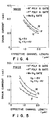
- Figures 4 and 5 are graphs showing relations between an effective channel length and a drain current in an NMOSFET and a PMOSFET, respectively.
- a curve M shows a characteristic of a device having a MoSi2 gate electrode according to the invention
- curves P and N show characteristics of devices having a conventional P+ polysilicon gate electrode and a conventional N+ polysilicon gate electrode, respectively, according to the prior art.
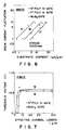
- Figure 6 shows a fluctuation of a drain current caused by a substrate current. Increase in the fluctuation of the drain current reduces reliability of the device.
- This graph indicates that the device according to the invention has higher reliability than the prior art device having an N+ polysilicon gate electrode though it has less reliability than the prior art device having a P+ polysilicon gate electrode.
- Figure 7 shows a relation between an effective channel length and a threshold voltage.
- a threshold voltage keeps a high level until an effective channel length rapidly decreases.
- the knee point of the curve M which corresponds to the device according to the invention, is located to the left of that of curve N, which corresponds to the prior device.
- the invention prevents the short channel effect.
- a MOSFET according to the invention adopts the buried channel structure and has a gate electrode made of materials having an intermediate Fermi level, the following improvement can be attained.
Landscapes
- Insulated Gate Type Field-Effect Transistor (AREA)
- Metal-Oxide And Bipolar Metal-Oxide Semiconductor Integrated Circuits (AREA)
Claims (2)
- Halbleiterelement mit kurzem Kanal, das ein Siliziumsubstrat (1) eines ersten Leitfähigkeitstyps, eine Sourceelektrode (3) und eine Drainelektrode (4) eines zweiten Leitfähigkeitstyps, die beide auf dem Substrat (1) gebildet sind, einen vergrabenen Kanal (7) des zweiten Leitfähigkeitstyps, der zwischen der Sourceelektrode (3) und der Drainelektrode (4) gebildet ist, und Gateelektrode (6) umfaßt, die über dem Kanal (7) mit Hilfe einer Isolierschicht (5) gebildet ist,
wobei die Gateelektrode (6) aus einem Material besteht, das ein Fermi-Niveau zwischen dem Leitungsband und dem Valenzband des Halbleiters aufweist,
dadurch gekennzeichnet, daß im Substrat (1) eine Störstellenkonzentration von mehr als 1x10¹⁷ cm⁻³ vorhanden ist. - Halbleiterelement mit kurzem Kanal nach Anspruch 1, bei dem die Gateelektrode aus Wolfram, Molybdän oder aus Siliziden dieser Metalle besteht.
Applications Claiming Priority (2)
| Application Number | Priority Date | Filing Date | Title |
|---|---|---|---|
| JP64406/86 | 1986-03-22 | ||
| JP61064406A JPS62219966A (ja) | 1986-03-22 | 1986-03-22 | 半導体装置 |
Publications (3)
| Publication Number | Publication Date |
|---|---|
| EP0239019A2 EP0239019A2 (de) | 1987-09-30 |
| EP0239019A3 EP0239019A3 (en) | 1989-11-08 |
| EP0239019B1 true EP0239019B1 (de) | 1993-12-22 |
Family
ID=13257395
Family Applications (1)
| Application Number | Title | Priority Date | Filing Date |
|---|---|---|---|
| EP87104093A Expired - Lifetime EP0239019B1 (de) | 1986-03-22 | 1987-03-20 | Feldeffekttransistoranordnungen |
Country Status (4)
| Country | Link |
|---|---|
| US (1) | US4841346A (de) |
| EP (1) | EP0239019B1 (de) |
| JP (1) | JPS62219966A (de) |
| DE (1) | DE3788525T2 (de) |
Families Citing this family (29)
| Publication number | Priority date | Publication date | Assignee | Title |
|---|---|---|---|---|
| US5122474A (en) * | 1988-06-23 | 1992-06-16 | Dallas Semiconductor Corporation | Method of fabricating a CMOS IC with reduced susceptibility to PMOS punchthrough |
| US5164805A (en) * | 1988-08-22 | 1992-11-17 | Massachusetts Institute Of Technology | Near-intrinsic thin-film SOI FETS |
| US4990974A (en) * | 1989-03-02 | 1991-02-05 | Thunderbird Technologies, Inc. | Fermi threshold field effect transistor |
| US5245207A (en) * | 1989-04-21 | 1993-09-14 | Nobuo Mikoshiba | Integrated circuit |
| CA2014296C (en) * | 1989-04-21 | 2000-08-01 | Nobuo Mikoshiba | Integrated circuit |
| JP2776891B2 (ja) * | 1989-06-19 | 1998-07-16 | 株式会社日立製作所 | 半導体集積回路装置 |
| GB2243948B (en) * | 1990-04-20 | 1994-06-08 | Nobuo Mikoshiba | Integrated circuit |
| KR920005242A (ko) * | 1990-08-20 | 1992-03-28 | 김광호 | 게이트-절연체-반도체의 구조를 가지는 트랜지스터의 제조방법 |
| US5440160A (en) * | 1992-01-28 | 1995-08-08 | Thunderbird Technologies, Inc. | High saturation current, low leakage current fermi threshold field effect transistor |
| US5369295A (en) * | 1992-01-28 | 1994-11-29 | Thunderbird Technologies, Inc. | Fermi threshold field effect transistor with reduced gate and diffusion capacitance |
| US5525822A (en) * | 1991-01-28 | 1996-06-11 | Thunderbird Technologies, Inc. | Fermi threshold field effect transistor including doping gradient regions |
| US5814869A (en) * | 1992-01-28 | 1998-09-29 | Thunderbird Technologies, Inc. | Short channel fermi-threshold field effect transistors |
| US5367186A (en) * | 1992-01-28 | 1994-11-22 | Thunderbird Technologies, Inc. | Bounded tub fermi threshold field effect transistor |
| US5786620A (en) * | 1992-01-28 | 1998-07-28 | Thunderbird Technologies, Inc. | Fermi-threshold field effect transistors including source/drain pocket implants and methods of fabricating same |
| US5543654A (en) * | 1992-01-28 | 1996-08-06 | Thunderbird Technologies, Inc. | Contoured-tub fermi-threshold field effect transistor and method of forming same |
| US5352914A (en) * | 1992-08-03 | 1994-10-04 | Hughes Aircraft Company | Field-effect transistor with structure for suppressing hot-electron effects, and method of fabricating the transistor |
| US5424226A (en) * | 1994-04-11 | 1995-06-13 | Xerox Corporation | Method of fabricating NMOS and PMOS FET's in a CMOS process |
| JP3553576B2 (ja) * | 1996-03-22 | 2004-08-11 | 株式会社ニコン | 固体撮像装置、mosトランジスタ及び寄生容量抑制方法 |
| US6424016B1 (en) * | 1996-05-24 | 2002-07-23 | Texas Instruments Incorporated | SOI DRAM having P-doped polysilicon gate for a memory pass transistor |
| US6246093B1 (en) | 1996-09-25 | 2001-06-12 | Lsi Logic Corporation | Hybrid surface/buried-channel MOSFET |
| US5874329A (en) * | 1996-12-05 | 1999-02-23 | Lsi Logic Corporation | Method for artificially-inducing reverse short-channel effects in deep sub-micron CMOS devices |
| JPH10189920A (ja) * | 1996-12-27 | 1998-07-21 | Toshiba Corp | 不揮発性半導体記憶装置及びその製造方法 |
| TW432636B (en) * | 1997-09-26 | 2001-05-01 | Thunderbird Tech Inc | Metal gate fermi-threshold field effect transistor |
| US6180464B1 (en) * | 1998-11-24 | 2001-01-30 | Advanced Micro Devices, Inc. | Metal oxide semiconductor device with localized laterally doped channel |
| FR2791181B1 (fr) * | 1999-03-19 | 2003-10-17 | France Telecom | Nouveaux transistor a grille metallique et canal enterre, contre-dope, et procede de fabrication |
| US6541829B2 (en) * | 1999-12-03 | 2003-04-01 | Kabushiki Kaisha Toshiba | Semiconductor device and method of manufacturing the same |
| US7064313B1 (en) | 2000-10-05 | 2006-06-20 | Ess Technology, Inc. | Gradual reset voltage reduction for resetting an image sensor |
| US6768149B1 (en) * | 2000-10-05 | 2004-07-27 | Ess Technology, Inc. | Tapered threshold reset FET for CMOS imagers |
| US7271457B2 (en) * | 2005-03-04 | 2007-09-18 | Bae Systems Information And Electronic Systems Integration Inc. | Abrupt channel doping profile for fermi threshold field effect transistors |
Family Cites Families (7)
| Publication number | Priority date | Publication date | Assignee | Title |
|---|---|---|---|---|
| GB1602361A (en) * | 1977-02-21 | 1981-11-11 | Zaidan Hojin Handotai Kenkyu | Semiconductor memory devices |
| JPS57194567A (en) * | 1981-05-27 | 1982-11-30 | Hitachi Ltd | Semiconductor memory device |
| JPS596577A (ja) * | 1982-07-05 | 1984-01-13 | Toshiba Corp | 半導体装置とその製造方法 |
| JPS59151464A (ja) * | 1983-02-17 | 1984-08-29 | Nec Corp | Misトランジスタ及びその製造方法 |
| DE3330851A1 (de) * | 1983-08-26 | 1985-03-14 | Siemens AG, 1000 Berlin und 8000 München | Verfahren zum herstellen von hochintegrierten komplementaeren mos-feldeffekttransistorschaltungen |
| JPS6050960A (ja) * | 1983-08-30 | 1985-03-22 | Toshiba Corp | 半導体装置 |
| JPH05165680A (ja) * | 1991-12-13 | 1993-07-02 | Mitsubishi Electric Corp | メモリ操作トレ−ス装置 |
-
1986
- 1986-03-22 JP JP61064406A patent/JPS62219966A/ja active Pending
-
1987
- 1987-03-20 EP EP87104093A patent/EP0239019B1/de not_active Expired - Lifetime
- 1987-03-20 US US07/028,627 patent/US4841346A/en not_active Expired - Lifetime
- 1987-03-20 DE DE3788525T patent/DE3788525T2/de not_active Expired - Fee Related
Also Published As
| Publication number | Publication date |
|---|---|
| DE3788525T2 (de) | 1994-05-19 |
| EP0239019A3 (en) | 1989-11-08 |
| JPS62219966A (ja) | 1987-09-28 |
| DE3788525D1 (de) | 1994-02-03 |
| EP0239019A2 (de) | 1987-09-30 |
| US4841346A (en) | 1989-06-20 |
Similar Documents
| Publication | Publication Date | Title |
|---|---|---|
| US4841346A (en) | Field-effect transistor devices | |
| Shang et al. | Self-aligned n-channel germanium MOSFETs with a thin Ge oxynitride gate dielectric and tungsten gate | |
| Kotaki et al. | Novel bulk dynamic threshold voltage MOSFET (B-DTMOS) with advanced isolation (SITOS) and gate to shallow-well contact (SSS-C) processes for ultra low power dual gate CMOS | |
| KR0180066B1 (ko) | 반도체장치 및 그 제조방법 | |
| US7939902B2 (en) | Field effect transistor having source and/or drain forming schottky or schottky-like contact with strained semiconductor substrate | |
| US6680224B2 (en) | Methods of forming and operating field effect transistors having gate and sub-gate electrodes | |
| KR100495023B1 (ko) | 반도체 장치 및 그 제조 방법 | |
| US20040262681A1 (en) | Semiconductor device | |
| JPH08181314A (ja) | 低閾値電圧mosトランジスタおよびその製造方法 | |
| US6380055B2 (en) | Dopant diffusion-retarding barrier region formed within polysilicon gate layer | |
| JP2002118175A (ja) | 半導体装置及びその製造方法 | |
| US6376323B1 (en) | Fabrication of gate of P-channel field effect transistor with added implantation before patterning of the gate | |
| US20080142910A1 (en) | Semiconductor device | |
| US11646361B2 (en) | Electrical isolation structure using reverse dopant implantation from source/drain region in semiconductor fin | |
| TWI861978B (zh) | 電晶體結構 | |
| Sai-Halasz et al. | Experimental technology and characterization of self-aligned 0.1 µm-gate-length low-temperature operation NMOS devices | |
| CN101364599B (zh) | Cmos结构和处理cmos结构的方法以及包括至少cmos电路的处理器 | |
| US6740935B2 (en) | Semiconductor device | |
| JPH02203566A (ja) | Mos型半導体装置 | |
| Momose et al. | 1.0-µm n-well CMOS/bipolar technology | |
| JP2876866B2 (ja) | 半導体装置 | |
| JPH0571190B2 (de) | ||
| CA2014296C (en) | Integrated circuit | |
| US7566604B2 (en) | Method of fabricating a dual-gate structure that prevents cut-through and lowered mobility | |
| JP2845899B2 (ja) | 半導体集積回路装置の製造方法 |
Legal Events
| Date | Code | Title | Description |
|---|---|---|---|
| PUAI | Public reference made under article 153(3) epc to a published international application that has entered the european phase |
Free format text: ORIGINAL CODE: 0009012 |
|
| 17P | Request for examination filed |
Effective date: 19870320 |
|
| AK | Designated contracting states |
Kind code of ref document: A2 Designated state(s): DE FR GB |
|
| PUAL | Search report despatched |
Free format text: ORIGINAL CODE: 0009013 |
|
| AK | Designated contracting states |
Kind code of ref document: A3 Designated state(s): DE FR GB |
|
| 17Q | First examination report despatched |
Effective date: 19910923 |
|
| GRAA | (expected) grant |
Free format text: ORIGINAL CODE: 0009210 |
|
| AK | Designated contracting states |
Kind code of ref document: B1 Designated state(s): DE FR GB |
|
| REF | Corresponds to: |
Ref document number: 3788525 Country of ref document: DE Date of ref document: 19940203 |
|
| ET | Fr: translation filed | ||
| PLBE | No opposition filed within time limit |
Free format text: ORIGINAL CODE: 0009261 |
|
| STAA | Information on the status of an ep patent application or granted ep patent |
Free format text: STATUS: NO OPPOSITION FILED WITHIN TIME LIMIT |
|
| 26N | No opposition filed | ||
| PGFP | Annual fee paid to national office [announced via postgrant information from national office to epo] |
Ref country code: DE Payment date: 19970401 Year of fee payment: 11 |
|
| PGFP | Annual fee paid to national office [announced via postgrant information from national office to epo] |
Ref country code: GB Payment date: 19980311 Year of fee payment: 12 |
|
| PG25 | Lapsed in a contracting state [announced via postgrant information from national office to epo] |
Ref country code: DE Free format text: LAPSE BECAUSE OF NON-PAYMENT OF DUE FEES Effective date: 19981201 |
|
| REG | Reference to a national code |
Ref country code: FR Ref legal event code: D6 |
|
| PG25 | Lapsed in a contracting state [announced via postgrant information from national office to epo] |
Ref country code: GB Free format text: LAPSE BECAUSE OF NON-PAYMENT OF DUE FEES Effective date: 19990320 |
|
| GBPC | Gb: european patent ceased through non-payment of renewal fee |
Effective date: 19990320 |
|
| PGFP | Annual fee paid to national office [announced via postgrant information from national office to epo] |
Ref country code: FR Payment date: 20060308 Year of fee payment: 20 |