EP0223876B1 - Poudre de cuivre revêtue d'oxyde - Google Patents
Poudre de cuivre revêtue d'oxyde Download PDFInfo
- Publication number
- EP0223876B1 EP0223876B1 EP85115009A EP85115009A EP0223876B1 EP 0223876 B1 EP0223876 B1 EP 0223876B1 EP 85115009 A EP85115009 A EP 85115009A EP 85115009 A EP85115009 A EP 85115009A EP 0223876 B1 EP0223876 B1 EP 0223876B1
- Authority
- EP
- European Patent Office
- Prior art keywords
- particles
- metal
- oxide
- copper
- compound
- Prior art date
- Legal status (The legal status is an assumption and is not a legal conclusion. Google has not performed a legal analysis and makes no representation as to the accuracy of the status listed.)
- Expired - Lifetime
Links
Images


Classifications
-
- H—ELECTRICITY
- H05—ELECTRIC TECHNIQUES NOT OTHERWISE PROVIDED FOR
- H05K—PRINTED CIRCUITS; CASINGS OR CONSTRUCTIONAL DETAILS OF ELECTRIC APPARATUS; MANUFACTURE OF ASSEMBLAGES OF ELECTRICAL COMPONENTS
- H05K1/00—Printed circuits
- H05K1/02—Details
- H05K1/09—Use of materials for the conductive, e.g. metallic pattern
- H05K1/092—Dispersed materials, e.g. conductive pastes or inks
-
- B—PERFORMING OPERATIONS; TRANSPORTING
- B22—CASTING; POWDER METALLURGY
- B22F—WORKING METALLIC POWDER; MANUFACTURE OF ARTICLES FROM METALLIC POWDER; MAKING METALLIC POWDER; APPARATUS OR DEVICES SPECIALLY ADAPTED FOR METALLIC POWDER
- B22F1/00—Metallic powder; Treatment of metallic powder, e.g. to facilitate working or to improve properties
- B22F1/16—Metallic particles coated with a non-metal
-
- C—CHEMISTRY; METALLURGY
- C09—DYES; PAINTS; POLISHES; NATURAL RESINS; ADHESIVES; COMPOSITIONS NOT OTHERWISE PROVIDED FOR; APPLICATIONS OF MATERIALS NOT OTHERWISE PROVIDED FOR
- C09D—COATING COMPOSITIONS, e.g. PAINTS, VARNISHES OR LACQUERS; FILLING PASTES; CHEMICAL PAINT OR INK REMOVERS; INKS; CORRECTING FLUIDS; WOODSTAINS; PASTES OR SOLIDS FOR COLOURING OR PRINTING; USE OF MATERIALS THEREFOR
- C09D5/00—Coating compositions, e.g. paints, varnishes or lacquers, characterised by their physical nature or the effects produced; Filling pastes
- C09D5/24—Electrically-conducting paints
-
- C—CHEMISTRY; METALLURGY
- C22—METALLURGY; FERROUS OR NON-FERROUS ALLOYS; TREATMENT OF ALLOYS OR NON-FERROUS METALS
- C22C—ALLOYS
- C22C1/00—Making non-ferrous alloys
- C22C1/10—Alloys containing non-metals
- C22C1/1026—Alloys containing non-metals starting from a solution or a suspension of (a) compound(s) of at least one of the alloy constituents
-
- H—ELECTRICITY
- H01—ELECTRIC ELEMENTS
- H01B—CABLES; CONDUCTORS; INSULATORS; SELECTION OF MATERIALS FOR THEIR CONDUCTIVE, INSULATING OR DIELECTRIC PROPERTIES
- H01B1/00—Conductors or conductive bodies characterised by the conductive materials; Selection of materials as conductors
- H01B1/02—Conductors or conductive bodies characterised by the conductive materials; Selection of materials as conductors mainly consisting of metals or alloys
- H01B1/026—Alloys based on copper
-
- Y—GENERAL TAGGING OF NEW TECHNOLOGICAL DEVELOPMENTS; GENERAL TAGGING OF CROSS-SECTIONAL TECHNOLOGIES SPANNING OVER SEVERAL SECTIONS OF THE IPC; TECHNICAL SUBJECTS COVERED BY FORMER USPC CROSS-REFERENCE ART COLLECTIONS [XRACs] AND DIGESTS
- Y10—TECHNICAL SUBJECTS COVERED BY FORMER USPC
- Y10T—TECHNICAL SUBJECTS COVERED BY FORMER US CLASSIFICATION
- Y10T428/00—Stock material or miscellaneous articles
- Y10T428/29—Coated or structually defined flake, particle, cell, strand, strand portion, rod, filament, macroscopic fiber or mass thereof
- Y10T428/2982—Particulate matter [e.g., sphere, flake, etc.]
- Y10T428/2991—Coated
Definitions
- the invention relates to metal oxide-coated copper metal powders which are especially suitable for conductors in multilayers.
- hybrid microcircuit refers to the interconnection and packaging of discrete electronic devices in a thick film or thin film network.
- the interconnections have been made by building a circuit or a number of circuits on a ceramic substrate.
- multilayers of this type have been made by printing alternating layers of copper thick film conductor materials and dielectric materials in a desired configuration on a rigid ceramic substrate such as alumina. Each of the dielectric layers is fired in a nonoxidizing atmosphere to effect densification of the dielectric material without oxidizing the copper conductive material before the next layer is applied. Because the substrate prevents lateral shrinkage, the finished multilayer structure remains flat. Therefore, the thermal coefficient of expansion (TCE) of the thick film conductor and dielectric materials need only approximate the TCE of the substrate in order to obtain relatively flat multilayer structures.
- TCE thermal coefficient of expansion
- This process involves the use of a tape fabricated from 92-94% wt. purity Al2O3 ceramic powder and a flexible polymeric binder, one or more layers of which are metallized with a patterned conductive layer, including punched vias, stacked and then laminated with heat and pressure. After lamination, the multilayer assemblage is cofired in a reducing atmosphere to produce the completed multilayer. As many as forty such alternating layers are used to form high density interconnections for use in various electronic hardware such as computer logic modules.
- Al2O3 Since Al2O3 is refractory, the conductor metals must be correspondingly refractory.
- W, Mo and Mo/Mn have been used as the conductive layer material for metallic traces and via interconnects. Particularly widely used for multilayers has been the system Al2O3/Mo-Mn.
- the use of the Al2O3/Mo-Mn system has several disadvantages.
- the conductivity of Mo-Mn is too low for modern high speed data processing equipment.
- Al2O3/Mo-Mn requires firing temperatures on the order of 1500°C in a wet H2 atmosphere to achieve proper densification of the Al2O3.
- Al2O3 has a temperature coefficient of expansion (TCE) which is twice that of Si.
- Suitable glasses are disclosed to be ß-spodumene (Li2O ⁇ Al2O3 ⁇ 4SiO2) and cordierite (2MgO ⁇ 2Al2O3 ⁇ 5SiO2). Both the spodumene and cordierite sinter below 1000°C.
- the multiple layers are cofired 3-5 hours at 775 ⁇ 10°C in a steam/H2 atmosphere to burn out the polymeric binder, after which the H2/H2O atmosphere is replaced by N2 and firing is completed at 930-970°C to achieve densification of the glass ceramic material. Because of the high sintering temperature, the structure shrinks about 15% and glass ceramic material is crystallized into cordierite ceramic.
- the fine copper powder begins to sinter and shrink when it reaches 400°C in the firing cycle, whereas the glass ceramic material does not sinter until it reaches 780°C. Because of this difference in the sintering and shrinking characteristics of the two materials, the multilayer tends to incur warping and bowing. For this reason, it has been difficult to produce cordierite/copper multilayer structures with the required degree of flatness. Thus, it would be very desirable to have a copper-based conductive material which would not incur sintering until it reached about 780°C and which would also have predictable shrinkage characteristics approaching those of green glass ceramic tape, i.e. about 15% shrinkage occurring between 700 and 970°C.
- US-A-3 320 057 discloses a process for forming a powdered metal mixture comprising the steps of wetting powdered metal particles, in particular copper particles, with a solvent solution of a soluble basic salt of a metal such as Al, Ti, Zr, heating the mixture to volatilize said solvent thus forming an oxide coating onto the metal and firing in particular under a reducing atmosphere.
- the invention is therefore directed in its primary aspect to particles of Cu-containing metal selected from the group consisting of Cu, Cu/Cd, Cu/Zr, Cu/Ti, Cu/Cr and mixtures thereof bearing a continuous coating of at least one metal oxide wherein the metal is selected from the group consisting of Si, Ti, Ce, Zr, Al, Ba, Sr, La, Mg, Ca, V, Ta and mixtures thereof having a free energy of formation more negative than -98 kcal/mole, a particle size of 0.5-20 ⁇ m in largest dimension and a surface area less than 1.0 m2/g.
- the invention is directed to a method for producing finely divided Cu-containing metal particles selected from the group consisting of Cu, Cu/Cd, Cu/Zr, Cu/Ti, Cu/Cr and mixtures thereof bearing a continuous coating of at least one metal oxide wherein the metal is selected from the group consisting of Si, Ti, Ce, Zr, Al, Ba, Sr, La, Mg, Ca, V, Ta and mixtures thereof comprising the sequential steps of:
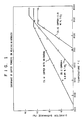
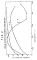
- Figures 1-4 are graphical representations of the effect of temperature upon the shrinkage of metal oxide-coated and uncoated copper particles
- Figure 4 is a blending curve for coated copper particles.
- Copper-containing thick film conductor compositions are, of course, well known in the art. They have, in fact, been formulated in a number of different ways for a wide variety of applications.
- U.S. 2,993,815 to Treptow is directed to a method of forming a copper conductive layer for printed circuits on a refractory substrate by screen printing a layer of 5-50 parts by weight copper or copper oxide and 1 part by weight of reduction-resistant glass frit dispersed in an organic medium.
- the conductive layer is formed by firing the applied paste in two stages at 500-1050°C. In the first firing stage, the glass is partially sintered in an oxidizing atmosphere and, in the second stage, the glass is completely sintered in a reducing atmosphere.
- the Grier patent, U.S. 4,072,771 is directed to a conductor composition comprising Cu particles, which have been preoxidized to form a surface layer of CuO, and glass frit dispersed in 15-25%, wt, organic medium.
- the oxide coating of the Cu particles constitutes 1-5% by wt. of the total solids (Cu oxide and glass).
- the patent is silent with respect to the use of oxides other than CuO.
- U.S. Patent Application, S.N. 526,400, Filed August 26, 1983, is directed to thick film copper conductor compositions for use with resistors or dielectrics, which are less susceptible to oxidation during firing in nonoxidizing conditions, comprising a conductive metal which is at least 28% copper, inorganic binder and a small amount of a noncuprous metal such as W, Mo, Re and alloys and mixtures thereof.
- unexamined Japanese Patent Application 57-71115 discloses an electrode paste comprising a dispersion of noble metal powder and organometallic powder dispersed in an organic medium.
- the organometallic compound forms very fine particles of corresponding metal oxides which are dispersed among the metal powder particles and are alleged to suppress growth of the metal particles.
- organometallic compounds can be used in the invention to coat the copper-containing particles so long as the oxide(s) of the metallic moiety thereof has a free energy of formation per gram atom of oxygen more negative than -98 kcal/mole. Therefore, the oxides of Si, Ti, Ce, Zr, Al, Ba, Li, Sr, La, Mg, Ca, V, Ta and mixtures thereof are used according to the invention.
- composition of the organometallic compound is not, strictly speaking, critical except to the extent that the compound must (1) be completely soluble in organic solvent, (2) contain an oxygen-metal linkage, and (3) be readily pyrolyzable in a nonoxidizing or reducing atmosphere.
- Suitable organometallic compounds includes hydrocarbyl metallates of the formula Me(OR)X and metal chelates such as those having the following structural formula: wherein X is a functional group containing oxygen or nitrogen and Y is C 2-3 alkyl.
- Titanium compounds of these two classes are quite readily available in commercial quantities and include such compounds as the following:
- titanium organometallic compounds are most available, nevertheless similar and analogous compounds exist for the other metals which are suitable for the invention. Among those are aluminum diisopropoxide acetate ester and tetraethoxy silane. Many others will be apparent to those skilled in the art of organometallic materials.
- the organometallic compound which is a precursor of the desired metal oxide, is deposited on the copper powder by dispersing the copper particles in a solution of the organometallic compound in an anhydrous volatile organic solvent.
- Suitable alcoholic solvents include methanol, ethanol, isopropanol and methyl ethyl ketone. Methylene chloride can also be used.
- the resultant oxide layer is in most instances on the order of 10-200 ⁇ in thickness and substantially continuous in nature. It is not, however, necessary that the coating be wholly continuous. Nevertheless, the extent of the coating must be such as to preclude any significant degree of metal-to-metal contact among the oxide-coated particles. Though thicker coatings tend to give more nearly complete particle coverage, the thickness of the oxide layer should not exceed about 1000 ⁇ in order to avoid substrate adhesion problems. Such layers are at most only about 100 atomic layers in thickness and therefore do not significantly change the diameter of the copper particles.
- both particle size and particle shape are very important.
- the copper-containing particles fall within the range of 0.5-20 ⁇ m and that the average particle size be 1-5 ⁇ m.
- the surface area of the particles becomes too high, which necessitates the use of excessive amounts of organic medium to obtain suitable printing viscosities.
- swelling and blistering of the printed Cu layer occurs when it is fired because it is very difficult to burn out high amounts of organic medium.
- the average particle size should be 1-5 ⁇ m.
- An average copper-containing particle size of 2-4 ⁇ m is preferred to attain even better properties in the fired film.
- the copper-containing particles used in the invention have a substantial degree of sphericity. That is, they must have a surface area-to-weight ratio of below about 1.0 m2/g. A ratio of 0.8 m2/g or lower is preferred and 0.2-0.5 m2/g is an especially preferred practical minimum range.
- the minimum possible surface-to-weight ratio for 2 ⁇ m size particles would be about 0.30 m2/g for perfect spheres. For 4 ⁇ m size spherical particles, the minimum possible surface area-to-weight ratio would be about 0.15 m2/g. However, as a practical matter, such perfect spheres are not obtainable.
- An important advantage of the invention is its use in making available Cu-containing particles which will have predictable shrinkage characteristics in practical applications.
- selected shrinkage characteristics can be achieved by blending oxide-coated particles having different shrinkages.
- oxide-coated particles having higher shrinkage e.g. 20%
- oxide-coated particles having lower shrinkage e.g., 13%
- the shrinkage of particles treated in accordance with the invention can be increased by mildly milling the particles.
- This operation can be carried out during the oxide coating step [Step (b)] or afterward. It is, however, preferred to carry out this additional operation during the oxide coating step. It should be recognized, however, that this mild milling step does not produce flake particles but merely more elliptical and truncated particles. Bead milling is frequently used for this purpose and is preferred.
- metal oxide-coated Cu particles were made by the following procedure:
- Shrinkage was determined by pressing 3 grams of Cu powder at 3000 psi (211 kg/cm2) in a 0.5 inch (1.27 cm) die. Copper pellets thusly formed were then heated for one hour in an N2 atmosphere to the indicated elevated temperatures. Shrinkage was calculated as the percent change in pellet diameter from measurements made before and after sintering.
Claims (6)
- Des particules d'un métal contenant du Cu choisi dans le groupe consistant en Cu, Cu/Cd, Cu/Zr, Cu/Ti, Cu/Cr et leurs mélanges, portant un revêtement continu d'au moins un oxyde métallique dans lequel le métal est choisi dans le groupe consistant en Si, Ti, Ce, Zr, Al, Ba, Sr, La, Mg, Ca, V, Ta, et leurs mélanges et ayant une energie libre de formation plus négative que -98 kcal/mole, une dimension particulaire de 0,5 à 20 µm dans la plus grande dimension et une aire superficielle inférieure à 1,0 m²/g
- Les particules revêtues suivant la revendication 1, dans lesquelles le métal contenant du Cu est du cuivre.
- Un procédé pour produire des particules finement divisées d'un métal contenant du cuivre choisi dans le groupe consistant en Cu, Cu/Cd, Cu/Zr, Cu/Ti, Cu/Cr et leurs mélanges, portant un revêtement continu d'au moins un oxyde métallique dans lequel le métal est choisi dans le groupe consistant en Si, Ti, Ce, Zr, Al, Ba, Sr, La, Mg, Ca, V, Ta et leurs mélanges, comprenant les étapes successives suivantes:(a) on disperse des particules d'un métal contenant du cuivre dans une solution comprenant un composé d'un métal dissous dans un solvant organique volatil,(b) tout en maintenant la dispersion sous agitation, on élimine le solvant par évaporation, de façon à déposer un revêtement du composé sur les particules de métal contenant du cuivre, et(c) on traite les particules de métal contenant du cuivre ainsi revêtues du composé dans une atmosphère réductrice à une température élevée et pendant un temps suffisant pour effectuer la réduction d'un quelconque oxyde de cuivre sur les particules de métal contenant du cuivre et la décomposition du composé en oxyde métallique correspondant, caractérisé en ce que le composé est un composé organométallique d'un métal dont l'oxyde a une énergie libre de formation plus négative que -98 kcal/mole.
- Un procédé suivant la revendication 3, dans lequel les particules d'un métal contenant du Cu revêtues d'oxyde sont soumises à un broyage léger pour effectuer un aplatissement des particules sans notablement modifier le rapport de l'aire superficielle au poids des particules.
- Le procédé suivant la revendication 4, dans lequel le broyage des particules est effectué pendant les étapes (a) et (b).
- Utilisation d'une dispersion dans un milieu organique des particules revêtues suivant la revendications 1, en tant que composition conductrice en couche épaisse imprimable.
Priority Applications (1)
| Application Number | Priority Date | Filing Date | Title |
|---|---|---|---|
| DE8585115009T DE3582070D1 (de) | 1985-11-27 | 1985-11-27 | Kupferpulver mit oxidueberzug. |
Applications Claiming Priority (1)
| Application Number | Priority Date | Filing Date | Title |
|---|---|---|---|
| US06/651,081 US4594181A (en) | 1984-09-17 | 1984-09-17 | Metal oxide-coated copper powder |
Publications (2)
| Publication Number | Publication Date |
|---|---|
| EP0223876A1 EP0223876A1 (fr) | 1987-06-03 |
| EP0223876B1 true EP0223876B1 (fr) | 1991-03-06 |
Family
ID=24611505
Family Applications (1)
| Application Number | Title | Priority Date | Filing Date |
|---|---|---|---|
| EP85115009A Expired - Lifetime EP0223876B1 (fr) | 1984-09-17 | 1985-11-27 | Poudre de cuivre revêtue d'oxyde |
Country Status (3)
| Country | Link |
|---|---|
| US (1) | US4594181A (fr) |
| EP (1) | EP0223876B1 (fr) |
| JP (1) | JPS62133002A (fr) |
Families Citing this family (32)
| Publication number | Priority date | Publication date | Assignee | Title |
|---|---|---|---|---|
| KR900008781B1 (ko) * | 1985-06-17 | 1990-11-29 | 마쯔시다덴기산교 가부시기가이샤 | 후막도체조성물 |
| US4716081A (en) * | 1985-07-19 | 1987-12-29 | Ercon, Inc. | Conductive compositions and conductive powders for use therein |
| US4810420A (en) * | 1986-10-02 | 1989-03-07 | General Electric Company | Thick film copper via-fill inks |
| CA1273853A (fr) * | 1986-12-17 | 1990-09-11 | Hitoshi Suzuki | Methode de production d'une carte ceramique a circuit |
| DE3806515C1 (fr) * | 1988-03-01 | 1989-07-20 | Du Pont De Nemours (Deutschland) Gmbh, 4000 Duesseldorf, De | |
| JPH02152105A (ja) * | 1988-12-01 | 1990-06-12 | Fujitsu Ltd | 導電材料およびその製造方法 |
| EP0406580B1 (fr) * | 1989-06-09 | 1996-09-04 | Matsushita Electric Industrial Co., Ltd. | Matériau composite et son procédé de préparation |
| JP2530934B2 (ja) * | 1990-05-10 | 1996-09-04 | 富士通株式会社 | バイヤホ―ル充填用金属粉集合体の製造方法 |
| US5283104A (en) * | 1991-03-20 | 1994-02-01 | International Business Machines Corporation | Via paste compositions and use thereof to form conductive vias in circuitized ceramic substrates |
| US5215610A (en) * | 1991-04-04 | 1993-06-01 | International Business Machines Corporation | Method for fabricating superconductor packages |
| JP2584911B2 (ja) * | 1991-06-18 | 1997-02-26 | 富士通株式会社 | ガラス−セラミック多層回路基板の製造方法 |
| US5925443A (en) * | 1991-09-10 | 1999-07-20 | International Business Machines Corporation | Copper-based paste containing copper aluminate for microstructural and shrinkage control of copper-filled vias |
| US5372749A (en) * | 1992-02-19 | 1994-12-13 | Beijing Technology Of Printing Research Institute Chinese | Method for surface treating conductive copper powder with a treating agent and coupler |
| US5296189A (en) * | 1992-04-28 | 1994-03-22 | International Business Machines Corporation | Method for producing metal powder with a uniform distribution of dispersants, method of uses thereof and structures fabricated therewith |
| US5336444A (en) * | 1992-05-29 | 1994-08-09 | International Business Machines Corporation | Ceramic via composition, multilayer ceramic circuit containing same, and process for using same |
| US5260519A (en) * | 1992-09-23 | 1993-11-09 | International Business Machines Corporation | Multilayer ceramic substrate with graded vias |
| US5293504A (en) * | 1992-09-23 | 1994-03-08 | International Business Machines Corporation | Multilayer ceramic substrate with capped vias |
| US5292477A (en) * | 1992-10-22 | 1994-03-08 | International Business Machines Corporation | Supersaturation method for producing metal powder with a uniform distribution of dispersants method of uses thereof and structures fabricated therewith |
| US5302562A (en) * | 1992-10-28 | 1994-04-12 | International Business Machines Corporation | Method of controlling the densification behavior of a metallic feature in a ceramic material |
| JP2913377B2 (ja) * | 1994-04-22 | 1999-06-28 | 株式会社巴川製紙所 | 粉体塗料 |
| US6338809B1 (en) * | 1997-02-24 | 2002-01-15 | Superior Micropowders Llc | Aerosol method and apparatus, particulate products, and electronic devices made therefrom |
| JP3511895B2 (ja) * | 1998-06-05 | 2004-03-29 | 株式会社村田製作所 | セラミック多層基板の製造方法 |
| US20030148024A1 (en) * | 2001-10-05 | 2003-08-07 | Kodas Toivo T. | Low viscosity precursor compositons and methods for the depositon of conductive electronic features |
| US6136419A (en) * | 1999-05-26 | 2000-10-24 | International Business Machines Corporation | Ceramic substrate having a sealed layer |
| JP4001438B2 (ja) * | 1999-05-31 | 2007-10-31 | 三井金属鉱業株式会社 | 複合銅微粉末の製造方法 |
| WO2002087809A1 (fr) * | 2001-04-27 | 2002-11-07 | Dowa Mining Co., Ltd. | Poudre de cuivre pour pate electroconductrice a excellente resistance a l'oxydation et procede de preparation |
| US20080199701A1 (en) * | 2003-02-25 | 2008-08-21 | Kuehnle Manfred R | Encapsulated nanoparticles for the absorption of electromagnetic energy |
| JP4059148B2 (ja) | 2003-06-02 | 2008-03-12 | 株式会社村田製作所 | 導電性ペーストおよびセラミック多層基板 |
| WO2005048667A1 (fr) | 2003-11-14 | 2005-05-26 | Murata Manufacturing Co., Ltd. | Pate conductrice et substrat en ceramique multicouche |
| JP4957465B2 (ja) * | 2006-09-11 | 2012-06-20 | 住友金属鉱山株式会社 | 酸化物被覆銅微粒子とその製造方法 |
| JP4854705B2 (ja) * | 2008-05-26 | 2012-01-18 | Dowaエレクトロニクス株式会社 | 導電ペースト用銀粉及びその銀粉を用いた導電ペースト |
| CN103514977A (zh) * | 2013-10-24 | 2014-01-15 | 云南云天化股份有限公司 | 一种金属导电颗粒及其制备方法、电极浆料 |
Family Cites Families (10)
| Publication number | Priority date | Publication date | Assignee | Title |
|---|---|---|---|---|
| US2993815A (en) * | 1959-05-25 | 1961-07-25 | Bell Telephone Labor Inc | Metallizing refractory substrates |
| US3320057A (en) * | 1964-12-31 | 1967-05-16 | Sylvania Electric Prod | Metal structure fabrication |
| US3988647A (en) * | 1974-09-27 | 1976-10-26 | General Electric Company | Method for making a circuit board and article made thereby |
| US4072771A (en) * | 1975-11-28 | 1978-02-07 | Bala Electronics Corporation | Copper thick film conductor |
| US4234367A (en) * | 1979-03-23 | 1980-11-18 | International Business Machines Corporation | Method of making multilayered glass-ceramic structures having an internal distribution of copper-based conductors |
| US4323483A (en) * | 1979-11-08 | 1982-04-06 | E. I. Du Pont De Nemours And Company | Mixed oxide bonded copper conductor compositions |
| JPS571115A (en) * | 1980-05-28 | 1982-01-06 | Okura Yusoki Co Ltd | Control method and unit for a reclinable conveyor |
| US4503090A (en) * | 1983-02-23 | 1985-03-05 | At&T Bell Laboratories | Thick film resistor circuits |
| US4521329A (en) * | 1983-06-20 | 1985-06-04 | E. I. Du Pont De Nemours And Company | Copper conductor compositions |
| US4514321A (en) * | 1983-08-25 | 1985-04-30 | E. I. Du Pont De Nemours And Company | Thick film conductor compositions |
-
1984
- 1984-09-17 US US06/651,081 patent/US4594181A/en not_active Expired - Lifetime
-
1985
- 1985-11-27 EP EP85115009A patent/EP0223876B1/fr not_active Expired - Lifetime
- 1985-12-06 JP JP60273589A patent/JPS62133002A/ja active Granted
Also Published As
| Publication number | Publication date |
|---|---|
| JPH0256402B2 (fr) | 1990-11-30 |
| US4594181A (en) | 1986-06-10 |
| JPS62133002A (ja) | 1987-06-16 |
| EP0223876A1 (fr) | 1987-06-03 |
Similar Documents
| Publication | Publication Date | Title |
|---|---|---|
| EP0223876B1 (fr) | Poudre de cuivre revêtue d'oxyde | |
| US4600604A (en) | Metal oxide-coated copper powder | |
| US6060165A (en) | Metal powder and process for preparing the same | |
| EP0916438B1 (fr) | Poudre de nickel et son procédé de préparation | |
| US5215610A (en) | Method for fabricating superconductor packages | |
| CA2021915A1 (fr) | Composition pour conducteur a film epais | |
| KR100259562B1 (ko) | 니켈분말 및 그 제조방법, 및 니켈분말을 사용한 도체 페이스트 및 페이스트를 사용하여 형성된 도체를 포함하는 적층세라믹 전자부품 또는 세라믹 다층기판 | |
| US5468445A (en) | Ceramic via composition, multilayer ceramic circuit containing same, and process for using same | |
| EP0992308B1 (fr) | Poudre composite de nickel et son procédé de préparation | |
| JP3414502B2 (ja) | 高温焼成対応貴金属粉末および導体ペースト | |
| EP0834370B1 (fr) | Poudre métallique revêtue et sa préparation par décomposition | |
| JP2004115295A (ja) | 高周波用低温焼結磁器組成物及びその製造方法 | |
| CA1240213A (fr) | Poudre de cuivre a enrobage d'oxyde de metal | |
| KR900000705B1 (ko) | 금속 산화물 피복 동분말 | |
| JP3833383B2 (ja) | 高周波用磁器組成物、高周波用磁器および高周波用磁器の製造方法 | |
| JP3754798B2 (ja) | 高周波用磁器組成物、高周波用磁器およびその製造方法 | |
| JP3754778B2 (ja) | 高周波用磁器組成物、高周波用磁器およびその製造方法 | |
| JP3628146B2 (ja) | 低温焼成磁器組成物および低温焼成磁器 | |
| JP3315182B2 (ja) | セラミック基板用組成物 | |
| JPH1116419A (ja) | 導電性ペースト及びこれを用いたセラミックス多層基板の製造方法 | |
| JP3631580B2 (ja) | 高周波用磁器組成物および高周波用磁器の製造方法 | |
| JPH0553282B2 (fr) | ||
| JPH0714746A (ja) | 低温焼成基板用コンデンサ材料の製造方法 | |
| JPS63215554A (ja) | 電気抵抗体ペ−スト及びその製造方法 |
Legal Events
| Date | Code | Title | Description |
|---|---|---|---|
| PUAI | Public reference made under article 153(3) epc to a published international application that has entered the european phase |
Free format text: ORIGINAL CODE: 0009012 |
|
| AK | Designated contracting states |
Kind code of ref document: A1 Designated state(s): BE DE FR GB IT LU NL |
|
| 17P | Request for examination filed |
Effective date: 19870617 |
|
| 17Q | First examination report despatched |
Effective date: 19880804 |
|
| GRAA | (expected) grant |
Free format text: ORIGINAL CODE: 0009210 |
|
| AK | Designated contracting states |
Kind code of ref document: B1 Designated state(s): BE DE FR GB IT LU NL |
|
| ITF | It: translation for a ep patent filed |
Owner name: ING. C. GREGORJ S.P.A. |
|
| ET | Fr: translation filed | ||
| REF | Corresponds to: |
Ref document number: 3582070 Country of ref document: DE Date of ref document: 19910411 |
|
| PLBE | No opposition filed within time limit |
Free format text: ORIGINAL CODE: 0009261 |
|
| STAA | Information on the status of an ep patent application or granted ep patent |
Free format text: STATUS: NO OPPOSITION FILED WITHIN TIME LIMIT |
|
| 26N | No opposition filed | ||
| PGFP | Annual fee paid to national office [announced via postgrant information from national office to epo] |
Ref country code: BE Payment date: 19921022 Year of fee payment: 8 |
|
| PGFP | Annual fee paid to national office [announced via postgrant information from national office to epo] |
Ref country code: LU Payment date: 19921027 Year of fee payment: 8 |
|
| PGFP | Annual fee paid to national office [announced via postgrant information from national office to epo] |
Ref country code: NL Payment date: 19921130 Year of fee payment: 8 |
|
| EPTA | Lu: last paid annual fee | ||
| PG25 | Lapsed in a contracting state [announced via postgrant information from national office to epo] |
Ref country code: LU Free format text: LAPSE BECAUSE OF NON-PAYMENT OF DUE FEES Effective date: 19931127 |
|
| PG25 | Lapsed in a contracting state [announced via postgrant information from national office to epo] |
Ref country code: BE Effective date: 19931130 |
|
| BERE | Be: lapsed |
Owner name: E.I. DU PONT DE NEMOURS AND CY Effective date: 19931130 |
|
| PG25 | Lapsed in a contracting state [announced via postgrant information from national office to epo] |
Ref country code: NL Effective date: 19940601 |
|
| NLV4 | Nl: lapsed or anulled due to non-payment of the annual fee | ||
| PGFP | Annual fee paid to national office [announced via postgrant information from national office to epo] |
Ref country code: FR Payment date: 19960903 Year of fee payment: 12 |
|
| PGFP | Annual fee paid to national office [announced via postgrant information from national office to epo] |
Ref country code: DE Payment date: 19960912 Year of fee payment: 12 |
|
| PGFP | Annual fee paid to national office [announced via postgrant information from national office to epo] |
Ref country code: GB Payment date: 19960926 Year of fee payment: 12 |
|
| PG25 | Lapsed in a contracting state [announced via postgrant information from national office to epo] |
Ref country code: GB Free format text: LAPSE BECAUSE OF NON-PAYMENT OF DUE FEES Effective date: 19971127 |
|
| PG25 | Lapsed in a contracting state [announced via postgrant information from national office to epo] |
Ref country code: FR Free format text: THE PATENT HAS BEEN ANNULLED BY A DECISION OF A NATIONAL AUTHORITY Effective date: 19971130 |
|
| GBPC | Gb: european patent ceased through non-payment of renewal fee |
Effective date: 19971127 |
|
| PG25 | Lapsed in a contracting state [announced via postgrant information from national office to epo] |
Ref country code: DE Free format text: LAPSE BECAUSE OF NON-PAYMENT OF DUE FEES Effective date: 19980801 |
|
| REG | Reference to a national code |
Ref country code: FR Ref legal event code: ST |