EP0223260B1 - Signalleseschaltungsanordnung für maskierte und überlappende lineare Bildsensoren - Google Patents
Signalleseschaltungsanordnung für maskierte und überlappende lineare Bildsensoren Download PDFInfo
- Publication number
- EP0223260B1 EP0223260B1 EP86116166A EP86116166A EP0223260B1 EP 0223260 B1 EP0223260 B1 EP 0223260B1 EP 86116166 A EP86116166 A EP 86116166A EP 86116166 A EP86116166 A EP 86116166A EP 0223260 B1 EP0223260 B1 EP 0223260B1
- Authority
- EP
- European Patent Office
- Prior art keywords
- linear image
- memory
- elements
- output signals
- written
- Prior art date
- Legal status (The legal status is an assumption and is not a legal conclusion. Google has not performed a legal analysis and makes no representation as to the accuracy of the status listed.)
- Expired - Lifetime
Links
- 230000015654 memory Effects 0.000 claims description 45
- 238000001465 metallisation Methods 0.000 claims description 10
- 238000000034 method Methods 0.000 claims description 5
- 238000006243 chemical reaction Methods 0.000 claims description 3
- 230000003111 delayed effect Effects 0.000 description 1
- 238000010586 diagram Methods 0.000 description 1
- 230000000873 masking effect Effects 0.000 description 1
- 230000003287 optical effect Effects 0.000 description 1
Images
Classifications
-
- H—ELECTRICITY
- H04—ELECTRIC COMMUNICATION TECHNIQUE
- H04N—PICTORIAL COMMUNICATION, e.g. TELEVISION
- H04N1/00—Scanning, transmission or reproduction of documents or the like, e.g. facsimile transmission; Details thereof
- H04N1/04—Scanning arrangements, i.e. arrangements for the displacement of active reading or reproducing elements relative to the original or reproducing medium, or vice versa
- H04N1/19—Scanning arrangements, i.e. arrangements for the displacement of active reading or reproducing elements relative to the original or reproducing medium, or vice versa using multi-element arrays
- H04N1/191—Scanning arrangements, i.e. arrangements for the displacement of active reading or reproducing elements relative to the original or reproducing medium, or vice versa using multi-element arrays the array comprising a one-dimensional array, or a combination of one-dimensional arrays, or a substantially one-dimensional array, e.g. an array of staggered elements
- H04N1/192—Simultaneously or substantially simultaneously scanning picture elements on one main scanning line
- H04N1/193—Simultaneously or substantially simultaneously scanning picture elements on one main scanning line using electrically scanned linear arrays, e.g. linear CCD arrays
- H04N1/1934—Combination of arrays
-
- H—ELECTRICITY
- H04—ELECTRIC COMMUNICATION TECHNIQUE
- H04N—PICTORIAL COMMUNICATION, e.g. TELEVISION
- H04N1/00—Scanning, transmission or reproduction of documents or the like, e.g. facsimile transmission; Details thereof
- H04N1/04—Scanning arrangements, i.e. arrangements for the displacement of active reading or reproducing elements relative to the original or reproducing medium, or vice versa
- H04N1/19—Scanning arrangements, i.e. arrangements for the displacement of active reading or reproducing elements relative to the original or reproducing medium, or vice versa using multi-element arrays
- H04N1/195—Scanning arrangements, i.e. arrangements for the displacement of active reading or reproducing elements relative to the original or reproducing medium, or vice versa using multi-element arrays the array comprising a two-dimensional array or a combination of two-dimensional arrays
- H04N1/19505—Scanning picture elements spaced apart from one another in at least one direction
- H04N1/1951—Scanning picture elements spaced apart from one another in at least one direction in one direction
-
- H—ELECTRICITY
- H04—ELECTRIC COMMUNICATION TECHNIQUE
- H04N—PICTORIAL COMMUNICATION, e.g. TELEVISION
- H04N25/00—Circuitry of solid-state image sensors [SSIS]; Control thereof
- H04N25/70—SSIS architectures; Circuits associated therewith
- H04N25/701—Line sensors
-
- H—ELECTRICITY
- H04—ELECTRIC COMMUNICATION TECHNIQUE
- H04N—PICTORIAL COMMUNICATION, e.g. TELEVISION
- H04N25/00—Circuitry of solid-state image sensors [SSIS]; Control thereof
- H04N25/70—SSIS architectures; Circuits associated therewith
- H04N25/701—Line sensors
- H04N25/7013—Line sensors using abutted sensors forming a long line
Definitions
- the present invention relates to an image reading circuit according to the precharacterizing part of claim 1 and to a method for reading signals from a plurality of linear image sensors according to the precharacterizing part of claim 6.
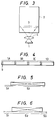
- the width of reading by a linear image sensor is usually about 2 to 3 cm. That width of reading is too short for the linear image sensor to read a document of size B5 or A4.
- the reading width 3 of a document 2 is larger than the length of a linear image sensor 1.
- a reduced image of the document 2 is focused on the photoelements of the linear image sensor 1 through a lens unit 4 and then read. For that reason, there is a disadvantage that the optical path length for making the reduced image on the linear image sensor and the size of a reading apparatus are both large.
- a plurality of linear image sensors 1A-1D are disposed in different reading positions so that the total length of the linear image sensors is equal to the reading width of the document. Since the photoresponse properties of the linear image sensors 1A-1D need to be set equal to each other, an opaque metalization mask 5 is provided on at least the first photoelement of each of the linear image sensors 1A-1D and the levels of the output signals of the opaque metalized light-intercepted portions of the sensors are made equal to each other to equalize the photoresponse properties of the sensors 1A-1D to each other. As a result, each of the linear image sensors 1A-1D sends out a normalizing signal S1, shown in Fig.
- a linear image sensor unit 10 is shown by a dot and dash line in Fig. 1 has been developed.
- the linear image sensor unit 10 five linear image sensors 11-15 are disposed so that their reading positions are different from each other not only in a main scanning direction but also in sub-scanning direction perpendicular to the principal linear image sensor direction, and opaque metalized portions 11M-15M of the linear image sensors 11-15 are overlapped with the rear portions of the preceding linear image sensors 11-15.
- the linear image sensor unit 10 sends out, as shown in Fig. 6, a signal S1 having a dark reference level corresponding to one of opaque metalization masks 11M-15M, an effective image signal S2, and a signal S3 corresponding to the overlap of the adjacent linear image sensors. It is a problem how to process the output signals of the linear image sensor unit 10.
- EP-A1-0 019 777 a circuit for electronically abutting parts of an electronic image is known.
- pixel data of two overlapping image sensors are stored into two associated memory areas whereby a controller assigns the addresses in the first and second memory areas at which the signals from the sensors are stored so that a correctly abutted electronic image can be obtained by successively reading out the contents of the first and second memory areas.
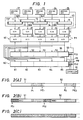
- Fig. 1 shows an embodiment of the present invention.
- Linear image sensors 11-15 which constitute a linear image sensor unit 10, are driven by drive circuits 21-25.
- the output signals of the linear image sensors 11-15 are entered into sample-and-hold circuits 31-35.
- the sampled and held signals are entered into the A/D converters 41-45 of an A/D converter unit 40 so that the signals are converted into digital signals. Since the reading positions of the linear image sensors 11-15 are different from each other in sub-scanning direction (transverse to the linear image sensors 11-15) as well as in a main scanning direction, the unprocessed output signals of the linear image sensors would not be identical with signals generated by reading along a single scanned line. However, in reality, the output signals are delayed in the linear image sensors 11-15 or the sample-and-hold circuits 31-35 so that the output signals are made identical with the signals generated by reading along the single scanned line.
- the A/D converted output of the A/D converter unit 40 is written into one of two line memories 50 and 60 switched by a control circuit not shown in the drawings.
- Serial image signals P1 or P2 are read out of the other of the line memories 60 and 50.
- the control circuit alternately interchanges the two line memories 50 and 60 for writing and reading so that the line memory 60 serves for reading and serial image signals PS2 are read out of the line memory 60 when the data from the A/D converter unit 40 are written into the line memory 50.
- the line memory 50 serves for reading and the already written data are sent as image signals PS1 out of the line memory 50 when the data from the A/D converter unit 40 are written into the line memory 60.
- the output signals of the linear image sensors 11-15 are sampled and held in parallel with each other by the sample-and-hold circuits 31-35.
- the sample-held values are subjected to A/D conversion by the A/D converters 41-45.
- the outputs of the A/D converters are written in parallel with each other into the corresponding storage elements of the line memory 50 or 60 so as to be stored as data therein.
- the image signals PS1 or PS2 are sent in series with each other out of the line memory 60 or 50 to which writing has been already finished.
- An image is read by the linear image sensors 11-15, starting with the positions of opaque metalization masks 11M-15M provided at the left-hand (illustrated in the drawings) ends of the linear image sensors 11-15.
- the digital signals obtained through the sample-and-hole circuits 31-35 and the A/D converters 41-45 are sequentially written into the storage elements 51-55 or 61-65 of the line memory 50 or 60, starting with an intermediate portion of each storage element rearwards and thereafter returning from the rearmost portion of the storage element to its foremost portion.
- the storage element 51 has a storage capacity for the number of the effective (unmasked and non-overlapped with the following linear image sensor 12) photoelements of the linear image sensor 11 and the storage element 52 has a storage capacity for the number of the effective photoelements of the linear image sensor 12.
- data obtained by digitizing the output signals of the linear image sensor 11 are written into the storage element 51 starting with a beginning address of P1 in the middle of the storage element 51
- data obtained by digitizing the output signals of the linear image sensor 12 are written into the storage element 52 starting with a beginning address of P2 in the middle of the storage element 52.
- a signal having a dark reference level and corresponding to the opaque metalization mask 11M is written into the storage element 51 at the beginning address P1, and an effective image signal is thereafter written into the storage element 51.
- Fig. 1 is shown an example of the control circuitry required for the invention.
- a controller 70 provides the necessary control signals. Timing signals are provided on a line 71 to all the elements.
- a read/write select signal on a line 72 is provided to the two line memories 50 and 60 and affects them in opposite ways. In synchronism with the timing signal, address signals are provided on line 73 to the line memories 50 and 60.
- each linear image sensor 11-15 has a total number N T of photoelements of which only a number N E are effective because of masking or overlap.
- each of the storage elements 51-55 and 61-65 contain N E storage locations.
- a CCD is a serial read-out device so that N T pulses of the timing signal on line 71 will completely read out the linear image sensors 11-15 beginning with the masked element.
- the line memory 50 or 60 which has been read enabled, sequentially reads out its contents in synchronism with the timing signals as the image signals PS1 or PS2.
- the effective image signal is written from the foremost portion of the storage element to its rearmost portion so that only the effective image signals are written into the line memory 50 or 60. For that reason, the unnecessary signals S1 of the dark reference level as shown in Fig. 5 are not included in the image signals PS1 or PS2 serially read out of the line memory 50 or 60.
- each of the storage elements of the line memory may exceed the number of the effective photoelements of the linear image sensor. In that case, reading is not performed out of the surplus storage portion of the storage element.
- a signal reading circuit is provided as described above, so that even if a plurality of linear image sensors are connected together in a long zigzag line, signals can be written into a memory while signals corresponding to the opaque metalization mask portions and overlapped portions of the linear image sensors are being removed. For that reason, serial image data corresponding to the document can be read out of a line memory. If line memories are alternately used for reading and writing, rapid image reading can be performed.
Landscapes
- Engineering & Computer Science (AREA)
- Multimedia (AREA)
- Signal Processing (AREA)
- Facsimile Scanning Arrangements (AREA)
Claims (6)
- Bildleseschaltkreis mit:
einer linearen Bildsensoreinheit (10) mit einer Vielzahl von linearen Bildsensoren (11-15), die in überlappender Weise entlang einer Hauptabtastrichtung des Bildleseschaltkreises angeordnet sind, wobei jeder lineare Bildsensor (11, 12, 13, 14, 15) eine Vielzahl von Photoelementen aufweist, die entlang der Hauptabtastrichtung angeordnet sind und eine metallisierte undurchsichtige Maske (11M-15M) aufweist, welche mindest ein Photoelement an einem ersten Ende des linearen Bildsensors überdeckt;
einer A/D-Wandlereinheit (40), die eine Vielzahl von A/D-Wandlern (41-55) aufweist zum Digitalisieren der Ausgangssignale der linearen Bildsensoren (11-15); und
einem Zeilenspeicher (50 oder 60), der eine Vielzahl von Speicherelementen (51-55 oder 61-65) aufweist, von denen jedes Ausgangssignale eines damit korrespondierenden A/D-Wandlers (41-45) empfängt und aus einer Anzahl von sequentiell angeordneten Speicherplatzelementen besteht, wobei diese Anzahl zumindest gleich der Anzahl der Photoelemente des korrespondierenden linearen Bildsensors (11-15) ist, welche nicht von der metallisierten undurchsichtigen Maske bedeckt sind,
dadurch gekennzeichnet, daß
eine Steuereinheit (70) an die A/D-Wandlereinheit (40) und an den Zeilenspeicher (50 oder 60) Steuersignale zur Verfügung stellt, um zu bewirken, daß die Ausgangssignale der A/D-Wandler sequentiell und in paralleler Weise in die Speicherplatzelemente der korrespondierenden Speicherelemente gbeschrieben werden, wobei die Ausgangssignale, die mit den maskierten Abschnitten der Sensorelemente korrespondieren, zuerst in die Speicherelemente geschrieben werden, wobei mit den Speicherplatzelementen begonnen wird, die sich an einem mittleren Abschnitt der Speicherelemente befinden und mit Speicherplatzelementen fortgefahren wird, die sich in Richtung zu den zweiten Enden der Speicherelemente erstrecken und wobei die Ausgangssignale des A/D-Wandlers, die mit den unmaskierten Abschnitten der Sensorelemente korrespondieren, dann nacheinander in die Speicherelemente geschrieben werden, wobei mit den Speicherplatzelemente begonnen wird, die an ersten Enden der Speicherelemente vorhanden sind und wobei zu den zweiten Enden hin fortgefahren wird, so daß die gespeicherten Ausgangssignale der maskierten Abschnitte überschrieben werden. - Bildleseschaltschreis nach Anspruch 1, gekennzeichnet durch eine Einrichtung zum sequentiellen Auslesen der Speicherplatzelemente.
- Bildleseschaltkreis nach Anspruch 2, dadurch gekennzeichnet, daß die Einrichtung zum sequentiellen Lesen die Speicherplatzelemente, vom ersten Ende eines Speicherelements beginnend, ausliest.
- Bildleseschaltkreis nach zumindest einem der vorhergehenden Ansprüche, dadurch gekennzeichnet, daß zwei Zeilenspeicher (50, 60) vorgesehen sind und eine Einrichtung zum Bewirken des Lesens des ersten Zeilenspeichers während des Beschreibens des zweiten Zeilenspeicher und umgekehrt, vorgesehen ist.
- Bildleseschaltkreis nach Anspruch 2, 3 oder 4, dadurch gekennzeichnet, daß die Leseeinrichtung in einer Sequenz eine Vielzahl von Speicherelementen erliest.
- Verfahren zum Auslesen von Signalen von einer Vielzahl von Bildsensoren (11-15), wobei die Bildsensoren in überlappender Weise entlang einer Hauptabtastrichtung angeordnet sind und wobei jeder lineare Bildsensor eine Vielzahl von Photoelementen aufweist und eine metallisierte undurchsichtige Maske (11M-15M) aufweist, welche zumindest ein Photoelement an einem ersten Ende des Sensors bedeckt, wobei das Verfahren die folgenden Schritte aufweist:
paralleles A/D-Wandeln der Ausgänge der linearen Bildsensoren, wobei jeder lineare Bildsensor sequentielle Signale von seinen Photoelementen ausgibt, beginnend von einem ersten Ende;
Einschreiben der analog-digital gewandelten Signale in eine Vielzahl von Speicherelementen (51-55 oder 61-65), die mit den linearen Bildsensoren korrespondieren, wobei jedes Bildelement aus einer Anzahl von sequentiell angeordneten Speicherplatzelementen besteht, wobei diese Anzahl zumindest gleich der Anzahl der Photoelemente des korrespondierenden linearen Bildsensors, welche nicht von der metallisierten undurchsichtigen Maske bedeckt sind, ist,
dadurch gekennzeichnet, daß
die Ausgangssignale, die mit den maskierten Photoelementen korrespondieren, in die Speicherelemente zuerst eingeschrieben werden, wobei bei jedem Speicherelement mit den Speicherplatzelementen begonnen wird, die sich an einem mittleren Abschnitt befinden und mit denjenigen Speicherplatzelementen fortgefahren wird, die sich in Richtung eines zweiten Endes befinden, und
wobei die Ausgangssignale, die mit den unmaskierten Photoelementen korrespondieren, dann hintereinander in die Speicherelemente eingeschrieben werden, wobei bei jedem Speicherelement mit den Speicherplatzelementen begonnen wird, die an einem ersten Ende angeordnet sind und wobei zu einem zweiten Ende hin fortgefahren wird, so daß die gespeicherten Ausgangssignale der maskierten Abschnitte überschrieben werden.
Applications Claiming Priority (2)
| Application Number | Priority Date | Filing Date | Title |
|---|---|---|---|
| JP262974/85 | 1985-11-22 | ||
| JP60262974A JPS62122461A (ja) | 1985-11-22 | 1985-11-22 | ラインセンサの読取回路 |
Publications (3)
| Publication Number | Publication Date |
|---|---|
| EP0223260A2 EP0223260A2 (de) | 1987-05-27 |
| EP0223260A3 EP0223260A3 (en) | 1989-03-08 |
| EP0223260B1 true EP0223260B1 (de) | 1994-02-02 |
Family
ID=17383133
Family Applications (1)
| Application Number | Title | Priority Date | Filing Date |
|---|---|---|---|
| EP86116166A Expired - Lifetime EP0223260B1 (de) | 1985-11-22 | 1986-11-21 | Signalleseschaltungsanordnung für maskierte und überlappende lineare Bildsensoren |
Country Status (4)
| Country | Link |
|---|---|
| US (1) | US4754338A (de) |
| EP (1) | EP0223260B1 (de) |
| JP (1) | JPS62122461A (de) |
| DE (1) | DE3689610T2 (de) |
Families Citing this family (9)
| Publication number | Priority date | Publication date | Assignee | Title |
|---|---|---|---|---|
| JPS63191469A (ja) * | 1987-02-03 | 1988-08-08 | Toshiba Corp | 画像読取装置 |
| JPS63234765A (ja) * | 1987-03-24 | 1988-09-30 | Dainippon Screen Mfg Co Ltd | 画像読取装置 |
| EP0292253B1 (de) * | 1987-05-22 | 1992-03-18 | Oki Electric Industry Company, Limited | Bildabtaster vom Kontakt-Typ |
| JPH01171361A (ja) * | 1987-12-25 | 1989-07-06 | Fuji Xerox Co Ltd | 原稿読取装置 |
| US4984085A (en) * | 1989-08-03 | 1991-01-08 | Allen-Bradley Company, Inc. | Image processor with dark current compensation |
| JPH0435177A (ja) * | 1990-05-25 | 1992-02-05 | Suzuki Motor Corp | Ccd駆動回路 |
| US5264945A (en) * | 1991-10-16 | 1993-11-23 | Eastman Kodak Company | Contact array scanners with circulating memory |
| CA2126064A1 (en) * | 1993-06-17 | 1994-12-18 | Jean-Francois Meunier | Apparatus and method for converting a visible image of an object into a digital representation |
| GB9622253D0 (en) * | 1996-10-25 | 1997-10-01 | Council Cent Lab Res Councils | Camera system |
Family Cites Families (16)
| Publication number | Priority date | Publication date | Assignee | Title |
|---|---|---|---|---|
| US4249217A (en) * | 1979-05-29 | 1981-02-03 | International Business Machines Corporation | Separated sensor array abutment |
| US4370641A (en) * | 1979-08-15 | 1983-01-25 | International Business Machines Corporation | Electronic control system |
| US4536801A (en) * | 1981-10-01 | 1985-08-20 | Banctec, Inc. | Video data compression system and method |
| DE3200838C2 (de) * | 1982-01-14 | 1984-09-06 | Messerschmitt-Bölkow-Blohm GmbH, 8012 Ottobrunn | Vorrichtung zum Auslesen von Detektorzeilen in ein- oder zweidimensionaler Anordnung |
| GB2122833B (en) * | 1982-06-24 | 1985-06-26 | Ferranti Plc | Radiation detecting apparatus |
| JPS5986379A (ja) * | 1982-11-08 | 1984-05-18 | Toshiba Corp | 光電変換装置 |
| DE3241752C2 (de) * | 1982-11-11 | 1984-09-06 | Messerschmitt-Bölkow-Blohm GmbH, 8012 Ottobrunn | Richtungsstabilisierte Bildfeldabtastung |
| FR2538651B1 (fr) * | 1982-12-23 | 1986-08-22 | Thomson Csf | Procede de modulation de la sensibilite d'un dispositif photosensible a transfert de ligne et dispositif mettant en oeuvre ce procede |
| US4639608A (en) * | 1983-05-18 | 1987-01-27 | Canon Kabushiki Kaisha | Image read-out apparatus with light source driving means |
| DE3427659A1 (de) * | 1983-07-29 | 1985-02-07 | Canon K.K., Tokio/Tokyo | Vorlagenleser |
| US4590521A (en) * | 1983-08-19 | 1986-05-20 | Advanced Micro Devices, Inc. | Picture element generator for facsimile receiver |
| US4691114A (en) * | 1984-02-29 | 1987-09-01 | Canon Kabushiki Kaisha | Original reader with variable magnification and time delay |
| CA1263175A (en) * | 1984-05-28 | 1989-11-21 | Hideyuki Miyazawa | Image reader for image processing apparatus |
| JPS6197619A (ja) * | 1984-10-19 | 1986-05-16 | Fuji Photo Film Co Ltd | 光学式リニアエンコ−ダ |
| US4652743A (en) * | 1984-11-30 | 1987-03-24 | Brother Kogyo Kabushiki Kaisha | Optical image-reading apparatus |
| DE3716152A1 (de) * | 1987-05-14 | 1988-11-24 | Standard Elektrik Lorenz Ag | An einer montageplatte schwimmend befestigte steckkupplung |
-
1985
- 1985-11-22 JP JP60262974A patent/JPS62122461A/ja active Granted
-
1986
- 1986-11-21 EP EP86116166A patent/EP0223260B1/de not_active Expired - Lifetime
- 1986-11-21 DE DE86116166T patent/DE3689610T2/de not_active Expired - Fee Related
- 1986-11-24 US US06/934,578 patent/US4754338A/en not_active Expired - Lifetime
Also Published As
| Publication number | Publication date |
|---|---|
| EP0223260A2 (de) | 1987-05-27 |
| US4754338A (en) | 1988-06-28 |
| DE3689610D1 (de) | 1994-03-17 |
| JPH0516781B2 (de) | 1993-03-05 |
| DE3689610T2 (de) | 1994-05-11 |
| EP0223260A3 (en) | 1989-03-08 |
| JPS62122461A (ja) | 1987-06-03 |
Similar Documents
| Publication | Publication Date | Title |
|---|---|---|
| US4644405A (en) | Method and apparatus for scanning a window in the image zone of a charge transfer device of the frame transfer type | |
| JP3408045B2 (ja) | 光電変換装置 | |
| DE3427659C2 (de) | ||
| US5689347A (en) | Signal processing apparatus | |
| US4424590A (en) | Document reader | |
| US4472744A (en) | Photoelectric converter apparatus | |
| EP0223260B1 (de) | Signalleseschaltungsanordnung für maskierte und überlappende lineare Bildsensoren | |
| GB2169769A (en) | Image processing apparatus | |
| US5550651A (en) | Image reading apparatus having a plurality of image sensors for reading a portion of an image a plurality of times | |
| EP0292253A2 (de) | Bildabtaster vom Kontakt-Typ | |
| US4939578A (en) | Method of driving multiple chip CCD image sensor | |
| US7471327B2 (en) | Image sensor array with variable resolution and high-speed output | |
| JPH02282868A (ja) | 複数チャンネル画像処理装置及び方法 | |
| JP3130822B2 (ja) | 画像入力装置 | |
| JP2002016762A (ja) | 画像読取方法及びその装置 | |
| JPS6117386B2 (de) | ||
| JPH0442870B2 (de) | ||
| JPS60171862A (ja) | 画像読取装置 | |
| JPS6031358A (ja) | 原稿読取装置 | |
| JPH11164087A (ja) | 固体撮像装置およびその駆動方法 | |
| JPS6031357A (ja) | 原稿読取装置 | |
| JP2953895B2 (ja) | 画像読取装置 | |
| JPH0312827B2 (de) | ||
| JP2889070B2 (ja) | 固体撮像装置の駆動方法 | |
| JPH0795795B2 (ja) | 原稿読み取り装置 |
Legal Events
| Date | Code | Title | Description |
|---|---|---|---|
| PUAI | Public reference made under article 153(3) epc to a published international application that has entered the european phase |
Free format text: ORIGINAL CODE: 0009012 |
|
| AK | Designated contracting states |
Kind code of ref document: A2 Designated state(s): DE FR GB |
|
| PUAL | Search report despatched |
Free format text: ORIGINAL CODE: 0009013 |
|
| AK | Designated contracting states |
Kind code of ref document: A3 Designated state(s): DE FR GB |
|
| 17P | Request for examination filed |
Effective date: 19890317 |
|
| 17Q | First examination report despatched |
Effective date: 19920320 |
|
| GRAA | (expected) grant |
Free format text: ORIGINAL CODE: 0009210 |
|
| AK | Designated contracting states |
Kind code of ref document: B1 Designated state(s): DE FR GB |
|
| REF | Corresponds to: |
Ref document number: 3689610 Country of ref document: DE Date of ref document: 19940317 |
|
| ET | Fr: translation filed | ||
| PLBE | No opposition filed within time limit |
Free format text: ORIGINAL CODE: 0009261 |
|
| STAA | Information on the status of an ep patent application or granted ep patent |
Free format text: STATUS: NO OPPOSITION FILED WITHIN TIME LIMIT |
|
| 26N | No opposition filed | ||
| REG | Reference to a national code |
Ref country code: GB Ref legal event code: IF02 |
|
| PGFP | Annual fee paid to national office [announced via postgrant information from national office to epo] |
Ref country code: FR Payment date: 20021108 Year of fee payment: 17 |
|
| PGFP | Annual fee paid to national office [announced via postgrant information from national office to epo] |
Ref country code: GB Payment date: 20021120 Year of fee payment: 17 |
|
| PGFP | Annual fee paid to national office [announced via postgrant information from national office to epo] |
Ref country code: DE Payment date: 20021121 Year of fee payment: 17 |
|
| PG25 | Lapsed in a contracting state [announced via postgrant information from national office to epo] |
Ref country code: GB Free format text: LAPSE BECAUSE OF NON-PAYMENT OF DUE FEES Effective date: 20031121 |
|
| PG25 | Lapsed in a contracting state [announced via postgrant information from national office to epo] |
Ref country code: DE Free format text: LAPSE BECAUSE OF NON-PAYMENT OF DUE FEES Effective date: 20040602 |
|
| GBPC | Gb: european patent ceased through non-payment of renewal fee |
Effective date: 20031121 |
|
| PG25 | Lapsed in a contracting state [announced via postgrant information from national office to epo] |
Ref country code: FR Free format text: LAPSE BECAUSE OF NON-PAYMENT OF DUE FEES Effective date: 20040730 |
|
| REG | Reference to a national code |
Ref country code: FR Ref legal event code: ST |