EP0221309B1 - Metallic magnetic recording medium - Google Patents
Metallic magnetic recording medium Download PDFInfo
- Publication number
- EP0221309B1 EP0221309B1 EP86112933A EP86112933A EP0221309B1 EP 0221309 B1 EP0221309 B1 EP 0221309B1 EP 86112933 A EP86112933 A EP 86112933A EP 86112933 A EP86112933 A EP 86112933A EP 0221309 B1 EP0221309 B1 EP 0221309B1
- Authority
- EP
- European Patent Office
- Prior art keywords
- layer
- silicon
- deposited
- recording medium
- carbon
- Prior art date
- Legal status (The legal status is an assumption and is not a legal conclusion. Google has not performed a legal analysis and makes no representation as to the accuracy of the status listed.)
- Expired - Lifetime
Links
- 230000005291 magnetic effect Effects 0.000 title claims description 101
- 239000010410 layer Substances 0.000 claims description 199
- XUIMIQQOPSSXEZ-UHFFFAOYSA-N Silicon Chemical compound [Si] XUIMIQQOPSSXEZ-UHFFFAOYSA-N 0.000 claims description 69
- 229910052710 silicon Inorganic materials 0.000 claims description 68
- 239000010703 silicon Substances 0.000 claims description 68
- 229910021385 hard carbon Inorganic materials 0.000 claims description 48
- 239000000758 substrate Substances 0.000 claims description 45
- 229910052799 carbon Inorganic materials 0.000 claims description 37
- OKTJSMMVPCPJKN-UHFFFAOYSA-N Carbon Chemical compound [C] OKTJSMMVPCPJKN-UHFFFAOYSA-N 0.000 claims description 36
- 238000000151 deposition Methods 0.000 claims description 28
- 230000008021 deposition Effects 0.000 claims description 24
- 229910021417 amorphous silicon Inorganic materials 0.000 claims description 19
- 238000000034 method Methods 0.000 claims description 11
- 229910021332 silicide Inorganic materials 0.000 claims description 8
- 229910010271 silicon carbide Inorganic materials 0.000 claims description 7
- 229910052751 metal Inorganic materials 0.000 claims description 6
- 239000011253 protective coating Substances 0.000 claims description 6
- 229910003481 amorphous carbon Inorganic materials 0.000 claims description 5
- 229910018540 Si C Inorganic materials 0.000 claims description 4
- 239000002356 single layer Substances 0.000 claims description 4
- 229910045601 alloy Inorganic materials 0.000 claims description 3
- 239000000956 alloy Substances 0.000 claims description 3
- 239000004593 Epoxy Substances 0.000 claims description 2
- 239000000919 ceramic Substances 0.000 claims description 2
- 125000003700 epoxy group Chemical group 0.000 claims description 2
- 239000011521 glass Substances 0.000 claims description 2
- 229920000647 polyepoxide Polymers 0.000 claims description 2
- 229920000642 polymer Polymers 0.000 claims description 2
- 239000010408 film Substances 0.000 description 43
- 239000011241 protective layer Substances 0.000 description 31
- 210000002381 plasma Anatomy 0.000 description 20
- 238000012360 testing method Methods 0.000 description 13
- UFHFLCQGNIYNRP-UHFFFAOYSA-N Hydrogen Chemical compound [H][H] UFHFLCQGNIYNRP-UHFFFAOYSA-N 0.000 description 10
- 239000001257 hydrogen Substances 0.000 description 10
- 229910052739 hydrogen Inorganic materials 0.000 description 10
- 230000001681 protective effect Effects 0.000 description 8
- 239000000203 mixture Substances 0.000 description 7
- XKRFYHLGVUSROY-UHFFFAOYSA-N Argon Chemical compound [Ar] XKRFYHLGVUSROY-UHFFFAOYSA-N 0.000 description 6
- BLRPTPMANUNPDV-UHFFFAOYSA-N Silane Chemical compound [SiH4] BLRPTPMANUNPDV-UHFFFAOYSA-N 0.000 description 6
- 238000005299 abrasion Methods 0.000 description 6
- HSFWRNGVRCDJHI-UHFFFAOYSA-N alpha-acetylene Natural products C#C HSFWRNGVRCDJHI-UHFFFAOYSA-N 0.000 description 6
- 239000011230 binding agent Substances 0.000 description 6
- 238000000576 coating method Methods 0.000 description 6
- 239000007789 gas Substances 0.000 description 6
- 239000000463 material Substances 0.000 description 6
- 230000001464 adherent effect Effects 0.000 description 5
- 239000011248 coating agent Substances 0.000 description 5
- 239000006249 magnetic particle Substances 0.000 description 5
- 239000002184 metal Substances 0.000 description 5
- 229910000077 silane Inorganic materials 0.000 description 5
- 125000002534 ethynyl group Chemical group [H]C#C* 0.000 description 4
- 238000002474 experimental method Methods 0.000 description 4
- 229910001004 magnetic alloy Inorganic materials 0.000 description 4
- 238000004519 manufacturing process Methods 0.000 description 4
- 229910052786 argon Inorganic materials 0.000 description 3
- 230000007423 decrease Effects 0.000 description 3
- 230000003247 decreasing effect Effects 0.000 description 3
- 238000005516 engineering process Methods 0.000 description 3
- 238000010348 incorporation Methods 0.000 description 3
- 239000002245 particle Substances 0.000 description 3
- FVBUAEGBCNSCDD-UHFFFAOYSA-N silicide(4-) Chemical compound [Si-4] FVBUAEGBCNSCDD-UHFFFAOYSA-N 0.000 description 3
- 238000004544 sputter deposition Methods 0.000 description 3
- 238000004627 transmission electron microscopy Methods 0.000 description 3
- VYPSYNLAJGMNEJ-UHFFFAOYSA-N Silicium dioxide Chemical compound O=[Si]=O VYPSYNLAJGMNEJ-UHFFFAOYSA-N 0.000 description 2
- 238000002441 X-ray diffraction Methods 0.000 description 2
- 239000000853 adhesive Substances 0.000 description 2
- 230000001070 adhesive effect Effects 0.000 description 2
- 229910052782 aluminium Inorganic materials 0.000 description 2
- 239000004411 aluminium Substances 0.000 description 2
- XAGFODPZIPBFFR-UHFFFAOYSA-N aluminium Chemical compound [Al] XAGFODPZIPBFFR-UHFFFAOYSA-N 0.000 description 2
- 238000004458 analytical method Methods 0.000 description 2
- 230000015572 biosynthetic process Effects 0.000 description 2
- 239000002131 composite material Substances 0.000 description 2
- 238000000354 decomposition reaction Methods 0.000 description 2
- 230000000694 effects Effects 0.000 description 2
- 239000000696 magnetic material Substances 0.000 description 2
- 230000006911 nucleation Effects 0.000 description 2
- 238000010899 nucleation Methods 0.000 description 2
- HBMJWWWQQXIZIP-UHFFFAOYSA-N silicon carbide Chemical compound [Si+]#[C-] HBMJWWWQQXIZIP-UHFFFAOYSA-N 0.000 description 2
- 239000010409 thin film Substances 0.000 description 2
- VLJQDHDVZJXNQL-UHFFFAOYSA-N 4-methyl-n-(oxomethylidene)benzenesulfonamide Chemical compound CC1=CC=C(S(=O)(=O)N=C=O)C=C1 VLJQDHDVZJXNQL-UHFFFAOYSA-N 0.000 description 1
- 229910019974 CrSi Inorganic materials 0.000 description 1
- RTAQQCXQSZGOHL-UHFFFAOYSA-N Titanium Chemical compound [Ti] RTAQQCXQSZGOHL-UHFFFAOYSA-N 0.000 description 1
- 239000000654 additive Substances 0.000 description 1
- 230000002411 adverse Effects 0.000 description 1
- PNEYBMLMFCGWSK-UHFFFAOYSA-N aluminium oxide Inorganic materials [O-2].[O-2].[O-2].[Al+3].[Al+3] PNEYBMLMFCGWSK-UHFFFAOYSA-N 0.000 description 1
- 238000013459 approach Methods 0.000 description 1
- 238000004140 cleaning Methods 0.000 description 1
- 229910052681 coesite Inorganic materials 0.000 description 1
- 238000005336 cracking Methods 0.000 description 1
- 229910052906 cristobalite Inorganic materials 0.000 description 1
- 238000002425 crystallisation Methods 0.000 description 1
- 229910003460 diamond Inorganic materials 0.000 description 1
- 239000010432 diamond Substances 0.000 description 1
- 230000008020 evaporation Effects 0.000 description 1
- 238000001704 evaporation Methods 0.000 description 1
- 230000005294 ferromagnetic effect Effects 0.000 description 1
- 239000003302 ferromagnetic material Substances 0.000 description 1
- 150000002500 ions Chemical class 0.000 description 1
- 238000004838 photoelectron emission spectroscopy Methods 0.000 description 1
- 229910021340 platinum monosilicide Inorganic materials 0.000 description 1
- 239000000843 powder Substances 0.000 description 1
- 238000012545 processing Methods 0.000 description 1
- 238000000926 separation method Methods 0.000 description 1
- 239000000377 silicon dioxide Substances 0.000 description 1
- 239000007787 solid Substances 0.000 description 1
- 229910052682 stishovite Inorganic materials 0.000 description 1
- 238000003860 storage Methods 0.000 description 1
- 239000010936 titanium Substances 0.000 description 1
- 229910052719 titanium Inorganic materials 0.000 description 1
- 229910052905 tridymite Inorganic materials 0.000 description 1
Images
Classifications
-
- G—PHYSICS
- G11—INFORMATION STORAGE
- G11B—INFORMATION STORAGE BASED ON RELATIVE MOVEMENT BETWEEN RECORD CARRIER AND TRANSDUCER
- G11B5/00—Recording by magnetisation or demagnetisation of a record carrier; Reproducing by magnetic means; Record carriers therefor
- G11B5/62—Record carriers characterised by the selection of the material
- G11B5/72—Protective coatings, e.g. anti-static or antifriction
- G11B5/726—Two or more protective coatings
- G11B5/7262—Inorganic protective coating
- G11B5/7264—Inorganic carbon protective coating, e.g. graphite, diamond like carbon or doped carbon
-
- Y—GENERAL TAGGING OF NEW TECHNOLOGICAL DEVELOPMENTS; GENERAL TAGGING OF CROSS-SECTIONAL TECHNOLOGIES SPANNING OVER SEVERAL SECTIONS OF THE IPC; TECHNICAL SUBJECTS COVERED BY FORMER USPC CROSS-REFERENCE ART COLLECTIONS [XRACs] AND DIGESTS
- Y10—TECHNICAL SUBJECTS COVERED BY FORMER USPC
- Y10S—TECHNICAL SUBJECTS COVERED BY FORMER USPC CROSS-REFERENCE ART COLLECTIONS [XRACs] AND DIGESTS
- Y10S428/00—Stock material or miscellaneous articles
- Y10S428/90—Magnetic feature
-
- Y—GENERAL TAGGING OF NEW TECHNOLOGICAL DEVELOPMENTS; GENERAL TAGGING OF CROSS-SECTIONAL TECHNOLOGIES SPANNING OVER SEVERAL SECTIONS OF THE IPC; TECHNICAL SUBJECTS COVERED BY FORMER USPC CROSS-REFERENCE ART COLLECTIONS [XRACs] AND DIGESTS
- Y10—TECHNICAL SUBJECTS COVERED BY FORMER USPC
- Y10T—TECHNICAL SUBJECTS COVERED BY FORMER US CLASSIFICATION
- Y10T428/00—Stock material or miscellaneous articles
- Y10T428/24—Structurally defined web or sheet [e.g., overall dimension, etc.]
- Y10T428/24942—Structurally defined web or sheet [e.g., overall dimension, etc.] including components having same physical characteristic in differing degree
- Y10T428/2495—Thickness [relative or absolute]
- Y10T428/24967—Absolute thicknesses specified
- Y10T428/24975—No layer or component greater than 5 mils thick
-
- Y—GENERAL TAGGING OF NEW TECHNOLOGICAL DEVELOPMENTS; GENERAL TAGGING OF CROSS-SECTIONAL TECHNOLOGIES SPANNING OVER SEVERAL SECTIONS OF THE IPC; TECHNICAL SUBJECTS COVERED BY FORMER USPC CROSS-REFERENCE ART COLLECTIONS [XRACs] AND DIGESTS
- Y10—TECHNICAL SUBJECTS COVERED BY FORMER USPC
- Y10T—TECHNICAL SUBJECTS COVERED BY FORMER US CLASSIFICATION
- Y10T428/00—Stock material or miscellaneous articles
- Y10T428/26—Web or sheet containing structurally defined element or component, the element or component having a specified physical dimension
- Y10T428/263—Coating layer not in excess of 5 mils thick or equivalent
- Y10T428/264—Up to 3 mils
- Y10T428/265—1 mil or less
-
- Y—GENERAL TAGGING OF NEW TECHNOLOGICAL DEVELOPMENTS; GENERAL TAGGING OF CROSS-SECTIONAL TECHNOLOGIES SPANNING OVER SEVERAL SECTIONS OF THE IPC; TECHNICAL SUBJECTS COVERED BY FORMER USPC CROSS-REFERENCE ART COLLECTIONS [XRACs] AND DIGESTS
- Y10—TECHNICAL SUBJECTS COVERED BY FORMER USPC
- Y10T—TECHNICAL SUBJECTS COVERED BY FORMER US CLASSIFICATION
- Y10T428/00—Stock material or miscellaneous articles
- Y10T428/30—Self-sustaining carbon mass or layer with impregnant or other layer
Definitions
- This invention relates to metallic magnetic recording media, and in particular to such media and methods for their production wherein an adherent, wear-resistant coating is provided on a metallic magnetic recording layer.
- Magnetic recording media are well known in the art, and include tapes, disks, drums, and other forms which are used for the storage of information. These recording media are generally comprised of a magnetic coating material deposited upon a permanent substrate.
- the magnetic coating material usually consists of a binder having ferromagnetic materials therein, or a metallic layer comprised of a magnetic material.
- An example of a magnetic recording medium comprised of a metallic magnetic layer is a hard disk having a substrate of aluminium or silicon and a magnetic metallic coating thereon, which can be an alloy such as GdCo, CoPtCr, CrV-CoPtCr, etc.
- a protective coating layer on the magnetic recording layer or to make the magnetic recording layer abrasion-resistant by incorporating hard particles in the magnetic recording layer.
- a hard protective overlayer on a magnetic recording layer where the recording layer can be comprised of either a ferromagnetic powder dispersed in a binder or a magnetic metallic film.
- the protective overlayer is comprised of wear-resistant non-magnetic particles of alumina, silicon carbide, diamond, etc., dispersed in an organic binder.
- the aforementioned Bruce et al article also describes the other approach to providing protection of a magnetic recording layer, i.e. the incorporation of particles into the magnetic recording layer to make it more abrasion-resistant. These particles are hard, non-magnetic particles of approximately 10 nm diameter which appear in the uppermost layer of the recording media.
- EP-A 0 026 496 discloses an alternative method of protecting a magnetic recording layer.
- EP-A 0 026 496 discloses a protective overcoating for a magnetic alloy thin-film recording disc that includes a disc-shaped base over which is formed a magnetic alloy film to provide a magnetic recording medium, comprising:
- the present invention provides improved wear-resistant coatings for metallic magnetic recording layers, where the protective layer is comprised of hard carbon which adheres very well to the metallic magnetic layer.
- the protective layer is comprised of hard carbon which adheres very well to the metallic magnetic layer.
- an interface layer of silicon is used.
- the silicon layer adheres very well to the underlying metallic magnetic layer, and can form metal silicides with this magnetic layer.
- the hard carbon layer adheres well to the silicon layer, and forms an interfacial layer of silicon-carbon bonds. It is not the intent of this invention to form a silicon carbide layer (which is known as a wear-resistant material), but rather to provide a hard carbon layer having good adhesion to the magnetic substrate, due to the silicon layer.
- the silicon layer is a monolayer to 50 nm (500 Angstroms) in thickness. It is only important that, after the silicon bonds to the metallic metal layer, that a continuous layer of silicon be available for bonding to the overlying hard carbon layer. Only a monolayer of continuous silicon is required for this purpose, as silicon and carbon can form Si-C bonds at room temperature. Thus, the silicon layer can be extremely thin and still provide strong adhesion to both the underlying metallic layer and the overlying hard carbon protective layer. This means that the recording head can be extremely close to the metallic magnetic recording layer, as is required in high density magnetic recording systems.
- the composite protective layer is comprised of silicon-SVC bonds-hard carbon, although it is feasible to have all of the silicon used in the formation of silicides with the underlying metallic magnetic layer and Si/C bonds with the overlying hard carbon layer.
- This protective layer is atomically smooth on its top surface and provides excellent protective properties against abrasion.
- hard carbon films are known as protective layers (K Enke, Thin Solid Films, 80, p. 227, 1981), these carbon films will not adhere to metallic magnetic recording layers.
- hard carbon layers which are themselves very desirable for their mechanical properties can be used as protective layers for metallic magnetic recording if an intermediate layer of silicon is used to provide the necessary adhesion between the underlying magnetic recording layer and the overlying hard carbon protective layer.
- both the silicon interfacial layer and the hard carbon protective layer are produced by plasma deposition in a single chamber, providing extreme ease of fabrication and fabrication reliability.
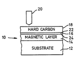
- the figure shows a structure representative of a magnetic recording medium including a metallic magnetic recording layer located on a substrate, and a composite protective layer comprised of a silicon interfacial layer and an overlying hard carbon protective layer.
- This type of layered structure can be incorporated into disks, tapes, cards, etc.
- the figure illustrates a recording structure of the type used in magnetic recording disks, tapes, cards, etc.
- the structure 10 is comprised of a substrate 12, a metallic magnetic recording layer 14, an interfacial layer 16 of silicon, and a hard carbon protective layer 18.
- the hard carbon layer 18 and the interfacial layer 16 provide a strongly-adherent, wear-resistant coating without unduly increasing the separation between the recording head 20 and the metallic magnetic recording layer 14.
- the specific compositions used for the substrate 12 and the metallic magnetic recording layer 14 can be varied, and include the types of materials generally known for these uses.
- the substrate 12 is typically glass, polymers, epoxies, ceramics, aluminium, or silicon.
- the metallic magnetic layer 14 is comprised of a thin film of a magnetic material or alloy, such as GdCo, CoPtCr, and CrV-CoPtCr, and the like.
- the nature of the substrate 12 and the metallic magnetic recording layer 14 is not critical to the invention, and other materials can be used as long as the magnetic recording layer 14 is comprised of a metallic film.
- hard carbon layers 18 are used a protective coatings over the metallic magnetic layer 14, and are made strongly adherent to the recording layer 14 by the use of an intermediate layer 16.
- This intermediate layer is silicon, which will form strong bonds with the underlying metallic magnetic layer 14 and with the overlying hard carbon layer 18.
- Silicon layer 16 serves as a nucleation layer, and its thickness is only such that a good bond will be formed to the underlying metallic layer 14 while leaving a continuous film of silicon for bonding to the overlying hard carbon layer 18.
- a few monolayers that is, a layer a few atoms thick
- the interface 24 between silicon , layer 16 and the metallic magnetic layer 14 may be comprised of metal silicides, such as PtSi and CrSi, where the phase of the metal silicide that is formed depends upon the deposition temperature (substrate temperature). For example, Pt silicide can form at 280 ° C, while Cr silicide can form at 500°C.
- the silicon interfacial layer 16 can be deposited by any known technique, such as evaporation, sputtering, or plasma deposition. Of these, plasma deposition is preferred since, with that technique, the same processing equipment and steps can be used to form the overlying hard carbon layer 18. In this manner, both the silicon layer 16 and the carbon layer 18 can be formed by plasma deposition without the requirement to break the vacuum in the system. The only steps to be undertaken are to change the source gases from, for example, silane, to acetylene (C 2 H 2 ).
- the plasma is comprised of hydrogen and the decomposition of mixtures of acetylene and hydrogen occurs by using an RF plasma.
- the substrate temperature for plasma deposition of carbon layer 18 should be below 325 ° C.
- the plasma deposition temperature for the silicon layer 16 is not critical, and can range from room temperature to 400 ° C, for example, 350 ° C.
- an amorphous silicon film, a-Si was deposited by plasma deposition from a gas mixture of 1% silane (SiH 4 ) in argon, at a flow rate of 25 sccm (standard cubic centimetres per minute), a total pressure of 125 1 1m (125 microns), and 5 W RF power.
- the substrates were kept at a bias of -150 VDC during the deposition of a-Si.
- the thickness of the deposited silicon layer 16 is not critical, as this layer is used as a nucleation, or interface, layer. Typically, silicon is deposited to a thickness of 1 - 5 nm .(10 to 50 Angstroms), although a possible range is from a monolayer to about 50 nm (500 Angstroms).
- the recording density of the metallic magnetic layer 14 has to be decreased to ensure that write and read operations can be adequately performed. This is opposite to the desired direction of the technology and therefore is unacceptable.
- the principle of the present invention - the provision of a strongly adherent and very protective layer - will still be present even though the thickness of the silicon layer is more than the required minimum.
- the lower 2 nm (20 Angstroms) or so of the silicon layer will strongly bond to the underlying metallic magnetic layer, while the uppermost 2 nm (20 Angstroms) or so of the silicon layer will form Si-C bonds with the overlying carbon layer 18.
- the hard carbon layer 18 is preferably deposited by plasma decomposition of a gas mixture, since this can be accomplished in the same vacuum system as the plasma deposition of silicon layer 16.
- a hard carbon layer can be deposited by other methods, such as sputtering.
- the thickness of the hard carbon layer 18 is usually about 25 nm (250 Angstroms), although its thickness can range from 2.5 nm (25 Angstroms) to 111m. If the hard carbon film 18 has a thickness in excess of about 1 ⁇ m, adverse stresses usually develop. Further, in order to provide high recording density, it is desirable to keep the carbon layer 18 as thin as possible while still retaining the necessary wear-resistant qualities, namely, atomic smoothness, ease of fabrication, and reproducibility. Carbon film 18 is an amorphous film which must be continuous in order to provide the necessary protective properties.
- amorphous silicon films have been deposited from a gas mixture of 1% silane in argon, at a flow rate of 25 sccm. A total pressure of 125 ⁇ .m (125 microns) was used, and 5 W of rf power were applied.
- substrates comprised of metallic magnetic layers
- the metallic magnetic layers were magnetic alloys of CoPtCr and CrV-CoPtCr. Approximately 0.5-2.5 nm (5-25 Angstroms) of silicon were deposited in this manner.
- the source gas was changed from silane in argon to acetylene (C 2 H 2 ).
- a 13.56 MHz rf plasma was used, where the plasma was produced by capacitive discharge between two parallel plates 7.62 cm (3 inches) in diameter, having 2.54 cm (1 inch) spacing between the plates.
- the silicon substrates Prior to carbon deposition, the silicon substrates were etched for 30 seconds in a 10% HF solution for removal of any surface oxide layer. The substrates were then exposed for 45 minutes to a hydrogen plasma in order to provide both reactive and sputtered cleaning of the growth surface and also a further reduction of the native oxide layer on the silicon substrates.
- the rf power was set at 5 watts (corresponding to a surface power density of 110 mW.cm- 2 ).
- the total pressure was held constant at 30 ⁇ .m (30 microns), with a total gas flow set at 6 sccm.
- the substrate electrode was kept at a negative DC bias of 150 VDC during deposition. Initial deposition runs were performed at a lower substrate bias of -70 VDC, ' but it was found that the adhesion of the carbon films to the substrates was better at the higher bias value. At substrate biases higher than this, arcing will occur in the reactor which will produce plasmas that are not stable.
- the carbon films will become graphitic and will soften significantly. For this reason, the substrate temperature are kept below 325°C, in order that a hard carbon layer will be deposited, which is required in order to provide the necessary protection of the underlying metallic layer.
- TEM Transmission electron microscopy
- Precleaning of the silicon substrates similar to plasma deposition of the hard carbon layer will provide better adherence between the silicon layer 16 and the carbon layer 18.
- the hydrogen plasma preclean does not, by itself, completely remove the native oxide from the silicon substrate.
- a superior protective coating is provided on the metallic magnetic recording layer, where the improved protective coating is comprised of a hard carbon layer deposited on a silicon layer located between the hard carbon layer and the underlying metallic magnetic layer.
- Plasma deposition is a preferred technique for producing this highly protective, strongly-adherent layer.
Landscapes
- Chemical & Material Sciences (AREA)
- Inorganic Chemistry (AREA)
- Magnetic Record Carriers (AREA)
- Manufacturing Of Magnetic Record Carriers (AREA)
Applications Claiming Priority (2)
| Application Number | Priority Date | Filing Date | Title |
|---|---|---|---|
| US06/793,517 US4647494A (en) | 1985-10-31 | 1985-10-31 | Silicon/carbon protection of metallic magnetic structures |
| US793517 | 1985-10-31 |
Publications (2)
| Publication Number | Publication Date |
|---|---|
| EP0221309A1 EP0221309A1 (en) | 1987-05-13 |
| EP0221309B1 true EP0221309B1 (en) | 1990-01-17 |
Family
ID=25160095
Family Applications (1)
| Application Number | Title | Priority Date | Filing Date |
|---|---|---|---|
| EP86112933A Expired - Lifetime EP0221309B1 (en) | 1985-10-31 | 1986-09-19 | Metallic magnetic recording medium |
Country Status (4)
| Country | Link |
|---|---|
| US (1) | US4647494A (enExample) |
| EP (1) | EP0221309B1 (enExample) |
| JP (1) | JPS62109222A (enExample) |
| DE (1) | DE3668391D1 (enExample) |
Families Citing this family (103)
| Publication number | Priority date | Publication date | Assignee | Title |
|---|---|---|---|---|
| US4774130A (en) * | 1985-01-17 | 1988-09-27 | Hitachi Metals, Ltd. | Magnetic recording medium |
| US4877677A (en) * | 1985-02-19 | 1989-10-31 | Matsushita Electric Industrial Co., Ltd. | Wear-protected device |
| JPS61242323A (ja) * | 1985-04-19 | 1986-10-28 | Fuji Electric Co Ltd | 磁気記録媒体 |
| US5300951A (en) * | 1985-11-28 | 1994-04-05 | Kabushiki Kaisha Toshiba | Member coated with ceramic material and method of manufacturing the same |
| US4755426A (en) * | 1986-01-18 | 1988-07-05 | Hitachi Maxell, Ltd. | Magnetic recording medium and production of the same |
| US4994321A (en) * | 1986-01-24 | 1991-02-19 | Fuji Photo Film Co., Ltd. | Perpendicular magnetic recording medium and the method for preparing the same |
| US4804590A (en) * | 1986-02-06 | 1989-02-14 | Nihon Shinku Gijutsu Kabushiki Kaisha | Abrasion resistant magnetic recording member |
| US4833031A (en) * | 1986-03-20 | 1989-05-23 | Matsushita Electric Industrial Co., Ltd. | Magnetic recording medium |
| JP2532209B2 (ja) * | 1986-04-04 | 1996-09-11 | ティーディーケイ株式会社 | 磁気記録媒体 |
| US4840844A (en) * | 1986-06-02 | 1989-06-20 | Hitachi, Ltd. | Magnetic recording medium |
| JPH07114016B2 (ja) * | 1986-06-12 | 1995-12-06 | 株式会社東芝 | 磁気記録媒体及びその製造方法 |
| DE3630419A1 (de) * | 1986-09-06 | 1988-03-10 | Kernforschungsanlage Juelich | Verfahren zur beschichtung von hoher waermebelastung ausgesetzten bauelementen mit einer amorphen wasserstoffhaltigen kohlenstoffschicht |
| JP2791015B2 (ja) * | 1986-12-24 | 1998-08-27 | 株式会社日立製作所 | 磁気記録媒体 |
| DE3644823A1 (de) * | 1986-12-31 | 1988-07-14 | Basf Ag | Magnetische aufzeichnungstraeger |
| US4861662A (en) * | 1987-02-03 | 1989-08-29 | Akashic Memories Corporation | Protective layer for magnetic disk |
| WO1988006334A1 (en) * | 1987-02-13 | 1988-08-25 | Akashic Memories Corporation | Surface coating for magnetic head |
| JPH0827940B2 (ja) * | 1987-04-24 | 1996-03-21 | 日本電気株式会社 | 磁気記憶体およびその製造方法 |
| JPS6476423A (en) * | 1987-09-17 | 1989-03-22 | Nec Corp | Magnetic disk |
| JPH01125720A (ja) * | 1987-11-10 | 1989-05-18 | Nec Corp | 磁気記憶体及びその製造方法 |
| JP2610469B2 (ja) * | 1988-02-26 | 1997-05-14 | 株式会社 半導体エネルギー研究所 | 炭素または炭素を主成分とする被膜を形成する方法 |
| US5190824A (en) | 1988-03-07 | 1993-03-02 | Semiconductor Energy Laboratory Co., Ltd. | Electrostatic-erasing abrasion-proof coating |
| US6224952B1 (en) * | 1988-03-07 | 2001-05-01 | Semiconductor Energy Laboratory Co., Ltd. | Electrostatic-erasing abrasion-proof coating and method for forming the same |
| US5275850A (en) * | 1988-04-20 | 1994-01-04 | Hitachi, Ltd. | Process for producing a magnetic disk having a metal containing hard carbon coating by plasma chemical vapor deposition under a negative self bias |
| US5030494A (en) * | 1989-01-26 | 1991-07-09 | International Business Machines Corporation | Carbon overcoat for a thin film magnetic recording disk containing discrete clusters of tungsten (W) or tungsten carbide (WC) which project from the surface of the overcoat |
| US5104694A (en) * | 1989-04-21 | 1992-04-14 | Nippon Telephone & Telegraph Corporation | Selective chemical vapor deposition of a metallic film on the silicon surface |
| US5266409A (en) * | 1989-04-28 | 1993-11-30 | Digital Equipment Corporation | Hydrogenated carbon compositions |
| US5031029A (en) * | 1990-04-04 | 1991-07-09 | International Business Machines Corporation | Copper device and use thereof with semiconductor devices |
| US5316844A (en) * | 1990-04-16 | 1994-05-31 | Hoya Electronics Corporation | Magnetic recording medium comprising an aluminum alloy substrate, now magnetic underlayers, magnetic layer, protective layer, particulate containing protective layer and lubricant layer |
| JP2910149B2 (ja) * | 1990-04-26 | 1999-06-23 | 松下電器産業株式会社 | 磁気記録媒体 |
| US5135808A (en) * | 1990-09-27 | 1992-08-04 | Diamonex, Incorporated | Abrasion wear resistant coated substrate product |
| US5637353A (en) * | 1990-09-27 | 1997-06-10 | Monsanto Company | Abrasion wear resistant coated substrate product |
| US5527596A (en) * | 1990-09-27 | 1996-06-18 | Diamonex, Incorporated | Abrasion wear resistant coated substrate product |
| US5164220A (en) * | 1990-10-29 | 1992-11-17 | Diamond Technologies Company | Method for treating diamonds to produce bondable diamonds for depositing same on a substrate |
| US5271802A (en) * | 1990-12-27 | 1993-12-21 | International Business Machines Corporation | Method for making a thin film magnetic head having a protective coating |
| JPH06101462B2 (ja) * | 1991-04-30 | 1994-12-12 | インターナショナル・ビジネス・マシーンズ・コーポレイション | 過フッ化炭化水素ポリマ膜を基板に接着する方法および 基板 |
| JPH05135344A (ja) * | 1991-05-17 | 1993-06-01 | Tdk Corp | 磁気記録媒体 |
| US5707717A (en) * | 1991-10-29 | 1998-01-13 | Tdk Corporation | Articles having diamond-like protective film |
| US5541003A (en) * | 1991-10-31 | 1996-07-30 | Tdk Corporation | Articles having diamond-like protective thin film |
| US5294518A (en) * | 1992-05-01 | 1994-03-15 | International Business Machines Corporation | Amorphous write-read optical storage memory |
| JP3099928B2 (ja) * | 1992-07-07 | 2000-10-16 | ティーディーケイ株式会社 | 磁気ディスク装置 |
| US5374412A (en) * | 1992-07-31 | 1994-12-20 | Cvd, Inc. | Highly polishable, highly thermally conductive silicon carbide |
| US5470447A (en) * | 1992-08-19 | 1995-11-28 | Stormedia, Inc. | Method for applying a protective coating on a magnetic recording head |
| US5609948A (en) * | 1992-08-21 | 1997-03-11 | Minnesota Mining And Manufacturing Company | Laminate containing diamond-like carbon and thin-film magnetic head assembly formed thereon |
| US5827613A (en) * | 1992-09-04 | 1998-10-27 | Tdk Corporation | Articles having diamond-like protective film and method of manufacturing the same |
| US5281851A (en) * | 1992-10-02 | 1994-01-25 | Hewlett-Packard Company | Integrated circuit packaging with reinforced leads |
| US5637373A (en) | 1992-11-19 | 1997-06-10 | Semiconductor Energy Laboratory Co., Ltd. | Magnetic recording medium |
| US6805941B1 (en) | 1992-11-19 | 2004-10-19 | Semiconductor Energy Laboratory Co., Ltd. | Magnetic recording medium |
| BE1006711A3 (nl) * | 1992-12-02 | 1994-11-22 | Vito | Werkwijze voor het aanbrengen van een diamantachtige koolstoflaag op staal, ijzer of legeringen daarvan. |
| US5344793A (en) * | 1993-03-05 | 1994-09-06 | Siemens Aktiengesellschaft | Formation of silicided junctions in deep sub-micron MOSFETs by defect enhanced CoSi2 formation |
| US5645900A (en) * | 1993-04-22 | 1997-07-08 | The United States Of America As Represented By The Administrator Of The National Aeronautics And Space Administration | Diamond composite films for protective coatings on metals and method of formation |
| US5626963A (en) * | 1993-07-07 | 1997-05-06 | Sanyo Electric Co., Ltd. | Hard-carbon-film-coated substrate and apparatus for forming the same |
| US5567512A (en) * | 1993-10-08 | 1996-10-22 | Hmt Technology Corporation | Thin carbon overcoat and method of its making |
| US5691010A (en) * | 1993-10-19 | 1997-11-25 | Sanyo Electric Co., Ltd. | Arc discharge plasma CVD method for forming diamond-like carbon films |
| US5482602A (en) * | 1993-11-04 | 1996-01-09 | United Technologies Corporation | Broad-beam ion deposition coating methods for depositing diamond-like-carbon coatings on dynamic surfaces |
| US5541566A (en) * | 1994-02-28 | 1996-07-30 | Olin Corporation | Diamond-like carbon coating for magnetic cores |
| US5508368A (en) * | 1994-03-03 | 1996-04-16 | Diamonex, Incorporated | Ion beam process for deposition of highly abrasion-resistant coatings |
| US5888593A (en) * | 1994-03-03 | 1999-03-30 | Monsanto Company | Ion beam process for deposition of highly wear-resistant optical coatings |
| US5846649A (en) * | 1994-03-03 | 1998-12-08 | Monsanto Company | Highly durable and abrasion-resistant dielectric coatings for lenses |
| US6087025A (en) * | 1994-03-29 | 2000-07-11 | Southwest Research Institute | Application of diamond-like carbon coatings to cutting surfaces of metal cutting tools |
| US5725573A (en) * | 1994-03-29 | 1998-03-10 | Southwest Research Institute | Medical implants made of metal alloys bearing cohesive diamond like carbon coatings |
| US5593719A (en) * | 1994-03-29 | 1997-01-14 | Southwest Research Institute | Treatments to reduce frictional wear between components made of ultra-high molecular weight polyethylene and metal alloys |
| US5605714A (en) * | 1994-03-29 | 1997-02-25 | Southwest Research Institute | Treatments to reduce thrombogeneticity in heart valves made from titanium and its alloys |
| US5731045A (en) * | 1996-01-26 | 1998-03-24 | Southwest Research Institute | Application of diamond-like carbon coatings to cobalt-cemented tungsten carbide components |
| US5984905A (en) | 1994-07-11 | 1999-11-16 | Southwest Research Institute | Non-irritating antimicrobial coating for medical implants and a process for preparing same |
| US5462784A (en) * | 1994-11-02 | 1995-10-31 | International Business Machines Corporation | Fluorinated diamond-like carbon protective coating for magnetic recording media devices |
| GB2295159B (en) * | 1994-11-21 | 1997-04-02 | Kao Corp | Magnetic recording medium |
| EP0718256B1 (en) * | 1994-12-23 | 1999-06-30 | Maruwa Ceramic Co., Ltd. | Ceramic sliding member and process of fabricating the same |
| EP0723944A1 (en) * | 1995-01-26 | 1996-07-31 | Optical Coating Laboratory, Inc. | Wear resistant windows |
| JPH09134515A (ja) * | 1995-09-05 | 1997-05-20 | Kao Corp | 磁気記録媒体 |
| KR0152251B1 (ko) * | 1995-11-02 | 1998-10-15 | 장진 | 층 .층 .층 제작 방법에 의한 유사다이아몬드 박막 제조 방법 |
| US5968679A (en) * | 1995-11-28 | 1999-10-19 | Hoya Corporation | Magnetic recording medium and method of manufacturing the same |
| US5731070A (en) * | 1995-12-20 | 1998-03-24 | Showa Denko Kabushiki Kaisha | Magnetic recording medium comprising a substrate, magnetic layer, and under layers including a silicon layer and a layer diffused with silicon |
| US5780119A (en) * | 1996-03-20 | 1998-07-14 | Southwest Research Institute | Treatments to reduce friction and wear on metal alloy components |
| US5858477A (en) * | 1996-12-10 | 1999-01-12 | Akashic Memories Corporation | Method for producing recording media having protective overcoats of highly tetrahedral amorphous carbon |
| US5922415A (en) * | 1996-06-20 | 1999-07-13 | Southwest Research Institute | Lubrication of magnetic disk storage media |
| US5948532A (en) * | 1996-12-10 | 1999-09-07 | International Business Machines Corporation | Cermet adhesion layer with carbonaceous wear layer for head/disk interfaces |
| US6066399A (en) | 1997-03-19 | 2000-05-23 | Sanyo Electric Co., Ltd. | Hard carbon thin film and method of forming the same |
| US6030904A (en) * | 1997-08-21 | 2000-02-29 | International Business Machines Corporation | Stabilization of low-k carbon-based dielectrics |
| US6040225A (en) * | 1997-08-29 | 2000-03-21 | The Whitaker Corporation | Method of fabricating polysilicon based resistors in Si-Ge heterojunction devices |
| US6130471A (en) * | 1997-08-29 | 2000-10-10 | The Whitaker Corporation | Ballasting of high power silicon-germanium heterojunction biploar transistors |
| US6726993B2 (en) * | 1997-12-02 | 2004-04-27 | Teer Coatings Limited | Carbon coatings, method and apparatus for applying them, and articles bearing such coatings |
| US6322880B1 (en) * | 1998-09-28 | 2001-11-27 | Seagate Technology Llc | Magneto-resistance recording media comprising a foundation layer and a C-overcoat |
| US6358636B1 (en) | 1998-11-05 | 2002-03-19 | Hmt Technology Corporation | Thin overlayer for magnetic recording disk |
| US6572958B1 (en) * | 1999-07-22 | 2003-06-03 | Seagate Technology Llc | Magnetic recording media comprising a silicon carbide corrosion barrier layer and a c-overcoat |
| WO2004008450A1 (en) * | 2002-06-05 | 2004-01-22 | Seagate Technology Llc | Protective overcoatings |
| US6764774B2 (en) | 2002-06-19 | 2004-07-20 | International Business Machines Corporation | Structures with improved adhesion to Si and C containing dielectrics and method for preparing the same |
| US7097745B2 (en) * | 2003-06-27 | 2006-08-29 | Seagate Technology, Llc | Method of forming a tunneling magnetoresistive head |
| US7067437B2 (en) * | 2003-09-12 | 2006-06-27 | International Business Machines Corporation | Structures with improved interfacial strength of SiCOH dielectrics and method for preparing the same |
| JP4427392B2 (ja) * | 2004-06-22 | 2010-03-03 | 株式会社東芝 | 磁気記録媒体、その製造方法及び磁気記録再生装置 |
| US8815060B2 (en) * | 2004-08-30 | 2014-08-26 | HGST Netherlands B.V. | Method for minimizing magnetically dead interfacial layer during COC process |
| JP3965404B2 (ja) * | 2004-10-18 | 2007-08-29 | ヒタチグローバルストレージテクノロジーズネザーランドビーブイ | 磁気記録媒体及びその製造方法 |
| US7329101B2 (en) * | 2004-12-29 | 2008-02-12 | General Electric Company | Ceramic composite with integrated compliance/wear layer |
| JP4649262B2 (ja) * | 2005-04-19 | 2011-03-09 | 株式会社東芝 | 磁気記録媒体の製造方法 |
| JP2007026506A (ja) * | 2005-07-14 | 2007-02-01 | Hitachi Global Storage Technologies Netherlands Bv | 磁気ヘッドスライダの製造方法及び磁気ヘッドスライダ |
| JP4585476B2 (ja) * | 2006-03-16 | 2010-11-24 | 株式会社東芝 | パターンド媒体および磁気記録装置 |
| JP4675812B2 (ja) * | 2006-03-30 | 2011-04-27 | 株式会社東芝 | 磁気記録媒体、磁気記録装置および磁気記録媒体の製造方法 |
| US7495865B2 (en) * | 2006-04-10 | 2009-02-24 | Seagate Technology Llc | Adhesion layer for protective overcoat |
| JP2008282512A (ja) * | 2007-05-14 | 2008-11-20 | Toshiba Corp | 磁気記録媒体及び磁気記録再生装置 |
| JP4382843B2 (ja) | 2007-09-26 | 2009-12-16 | 株式会社東芝 | 磁気記録媒体およびその製造方法 |
| EP2459913B1 (en) | 2009-07-29 | 2018-09-05 | Waters Technologies Corporation | Rotary shear injector valve with coated stator surface |
| US8687323B2 (en) | 2011-10-12 | 2014-04-01 | HGST Netherlands B.V. | Magnetic media disk anticorrosion overcoat with titanium and silicon based layers |
| JP5392375B2 (ja) * | 2012-05-07 | 2014-01-22 | 富士電機株式会社 | 記録媒体 |
| US9045348B2 (en) | 2012-08-29 | 2015-06-02 | HGST Netherlands B.V. | Titanium-silicon protective film composition and apparatus |
Family Cites Families (11)
| Publication number | Priority date | Publication date | Assignee | Title |
|---|---|---|---|---|
| US4411963A (en) * | 1976-10-29 | 1983-10-25 | Aine Harry E | Thin film recording and method of making |
| DE3027162A1 (de) * | 1979-07-23 | 1981-02-19 | Datapoint Corp | Speicherplatte mit einer duennen magnetischen legierungsschicht und verfahren zu ihrer herstellung |
| JPS5634143A (en) * | 1979-08-25 | 1981-04-06 | Hitachi Maxell Ltd | Magnetic recording medium |
| US4503125A (en) * | 1979-10-01 | 1985-03-05 | Xebec, Inc. | Protective overcoating for magnetic recording discs and method for forming the same |
| EP0026496B1 (en) * | 1979-10-01 | 1984-08-15 | Xebec | Magnetic recording disc and method for forming a protective overcoating thereon |
| US4376963A (en) * | 1980-12-19 | 1983-03-15 | International Business Machines Corporation | Composite magnetic recording disk |
| DE3210866C2 (de) * | 1981-03-24 | 1985-01-17 | Nippon Electric Co., Ltd., Tokio/Tokyo | Magnetischer Aufzeichnungsträger und Verfahren zu seiner Herstellung |
| US4542071A (en) * | 1983-07-14 | 1985-09-17 | International Business Machines Corporation | Lubricated magnetic recording disk |
| US4554217A (en) * | 1984-09-20 | 1985-11-19 | Verbatim Corporation | Process for creating wear and corrosion resistant film for magnetic recording media |
| US4774130A (en) * | 1985-01-17 | 1988-09-27 | Hitachi Metals, Ltd. | Magnetic recording medium |
| JPS61242323A (ja) * | 1985-04-19 | 1986-10-28 | Fuji Electric Co Ltd | 磁気記録媒体 |
-
1985
- 1985-10-31 US US06/793,517 patent/US4647494A/en not_active Expired - Lifetime
-
1986
- 1986-09-19 JP JP61219912A patent/JPS62109222A/ja active Granted
- 1986-09-19 EP EP86112933A patent/EP0221309B1/en not_active Expired - Lifetime
- 1986-09-19 DE DE8686112933T patent/DE3668391D1/de not_active Expired - Lifetime
Also Published As
| Publication number | Publication date |
|---|---|
| JPH0416853B2 (enExample) | 1992-03-25 |
| EP0221309A1 (en) | 1987-05-13 |
| JPS62109222A (ja) | 1987-05-20 |
| US4647494A (en) | 1987-03-03 |
| DE3668391D1 (de) | 1990-02-22 |
Similar Documents
| Publication | Publication Date | Title |
|---|---|---|
| EP0221309B1 (en) | Metallic magnetic recording medium | |
| JP3357313B2 (ja) | 薄膜磁気ヘッド、薄膜磁気ヘッド用基板、および薄膜磁気ヘッド用基板の製造方法 | |
| EP0239028B1 (en) | Magnetic recording medium | |
| US6086796A (en) | Diamond-like carbon over-coats for optical recording media devices and method thereof | |
| EP0293662B1 (en) | A process for making a thin film metal alloy magnetic recording disk with a hydrogenated carbon overcoat | |
| EP0275455B1 (en) | A thin film medium for horizontal magnetic recording having an improved cobalt-based alloy magnetic layer | |
| HK138994A (en) | A magnetic recording medium | |
| US6277484B1 (en) | Magnetic recording media and method of producing the same | |
| US5705287A (en) | Magnetic recording disk with metal nitride texturing layer | |
| JP5103005B2 (ja) | 垂直磁気記録媒体及びその製造方法 | |
| Cotell et al. | Effect of ion energy on the mechanical properties of ion beam assisted deposition (IBAD) wear resistant coatings | |
| KR19990077288A (ko) | 이결정 클러스터 자기 기록 매체 | |
| WO1998010115A1 (en) | Silicon-doped diamond-like carbon coatings for magnetic transducers and for magnetic recording media | |
| US20090208778A1 (en) | Patterned magnetic recording medium and method for manufacturing same | |
| US5078846A (en) | Process for forming hafnia and zirconia based protective films on longitudinal magnetic recording media | |
| EP0547820B1 (en) | A magnetic recording disk having an improved protective overcoat | |
| US5759617A (en) | Production process for a hard disk magnetic recording medium | |
| JP2623785B2 (ja) | 磁気ディスク | |
| Hoshi et al. | Suppression of cone formation on carbon target during sputtering | |
| EP0422547B1 (en) | Magnetic recording medium | |
| JP2001176059A (ja) | 磁気記録媒体 | |
| JP2621133B2 (ja) | 磁気記録媒体及びその製造方法 | |
| Xie | Synthesis and Characterization of Amorphous Carbon Films for Magnetic Storage Technology | |
| JPH03245319A (ja) | 磁気ディスク、その製造方法およびそれを用いた磁気ディスク装置 | |
| JP2901706B2 (ja) | 磁気記録媒体および磁気ディスク装置 |
Legal Events
| Date | Code | Title | Description |
|---|---|---|---|
| PUAI | Public reference made under article 153(3) epc to a published international application that has entered the european phase |
Free format text: ORIGINAL CODE: 0009012 |
|
| AK | Designated contracting states |
Kind code of ref document: A1 Designated state(s): DE FR GB IT |
|
| 17P | Request for examination filed |
Effective date: 19870821 |
|
| 17Q | First examination report despatched |
Effective date: 19880216 |
|
| GRAA | (expected) grant |
Free format text: ORIGINAL CODE: 0009210 |
|
| AK | Designated contracting states |
Kind code of ref document: B1 Designated state(s): DE FR GB IT |
|
| REF | Corresponds to: |
Ref document number: 3668391 Country of ref document: DE Date of ref document: 19900222 |
|
| ET | Fr: translation filed | ||
| ITF | It: translation for a ep patent filed | ||
| PLBE | No opposition filed within time limit |
Free format text: ORIGINAL CODE: 0009261 |
|
| STAA | Information on the status of an ep patent application or granted ep patent |
Free format text: STATUS: NO OPPOSITION FILED WITHIN TIME LIMIT |
|
| 26N | No opposition filed | ||
| ITTA | It: last paid annual fee | ||
| PGFP | Annual fee paid to national office [announced via postgrant information from national office to epo] |
Ref country code: GB Payment date: 19930826 Year of fee payment: 8 |
|
| PGFP | Annual fee paid to national office [announced via postgrant information from national office to epo] |
Ref country code: FR Payment date: 19930830 Year of fee payment: 8 |
|
| PGFP | Annual fee paid to national office [announced via postgrant information from national office to epo] |
Ref country code: DE Payment date: 19930923 Year of fee payment: 8 |
|
| PG25 | Lapsed in a contracting state [announced via postgrant information from national office to epo] |
Ref country code: GB Effective date: 19940919 |
|
| GBPC | Gb: european patent ceased through non-payment of renewal fee |
Effective date: 19940919 |
|
| PG25 | Lapsed in a contracting state [announced via postgrant information from national office to epo] |
Ref country code: FR Effective date: 19950531 |
|
| PG25 | Lapsed in a contracting state [announced via postgrant information from national office to epo] |
Ref country code: DE Effective date: 19950601 |
|
| REG | Reference to a national code |
Ref country code: FR Ref legal event code: ST |
|
| PG25 | Lapsed in a contracting state [announced via postgrant information from national office to epo] |
Ref country code: IT Free format text: LAPSE BECAUSE OF NON-PAYMENT OF DUE FEES;WARNING: LAPSES OF ITALIAN PATENTS WITH EFFECTIVE DATE BEFORE 2007 MAY HAVE OCCURRED AT ANY TIME BEFORE 2007. THE CORRECT EFFECTIVE DATE MAY BE DIFFERENT FROM THE ONE RECORDED. Effective date: 20050919 |