EP0213309A2 - Circuit de contrôle automatique de gain - Google Patents
Circuit de contrôle automatique de gain Download PDFInfo
- Publication number
- EP0213309A2 EP0213309A2 EP86108803A EP86108803A EP0213309A2 EP 0213309 A2 EP0213309 A2 EP 0213309A2 EP 86108803 A EP86108803 A EP 86108803A EP 86108803 A EP86108803 A EP 86108803A EP 0213309 A2 EP0213309 A2 EP 0213309A2
- Authority
- EP
- European Patent Office
- Prior art keywords
- level
- signals
- signal
- demodulator
- output
- Prior art date
- Legal status (The legal status is an assumption and is not a legal conclusion. Google has not performed a legal analysis and makes no representation as to the accuracy of the status listed.)
- Granted
Links
Images


Classifications
-
- H—ELECTRICITY
- H04—ELECTRIC COMMUNICATION TECHNIQUE
- H04L—TRANSMISSION OF DIGITAL INFORMATION, e.g. TELEGRAPHIC COMMUNICATION
- H04L27/00—Modulated-carrier systems
- H04L27/01—Equalisers
-
- H—ELECTRICITY
- H04—ELECTRIC COMMUNICATION TECHNIQUE
- H04L—TRANSMISSION OF DIGITAL INFORMATION, e.g. TELEGRAPHIC COMMUNICATION
- H04L25/00—Baseband systems
- H04L25/02—Details ; arrangements for supplying electrical power along data transmission lines
- H04L25/06—Dc level restoring means; Bias distortion correction ; Decision circuits providing symbol by symbol detection
- H04L25/061—Dc level restoring means; Bias distortion correction ; Decision circuits providing symbol by symbol detection providing hard decisions only; arrangements for tracking or suppressing unwanted low frequency components, e.g. removal of dc offset
- H04L25/063—Setting decision thresholds using feedback techniques only
- H04L25/064—Subtraction of the threshold from the signal, which is then compared to a supplementary fixed threshold
-
- H—ELECTRICITY
- H04—ELECTRIC COMMUNICATION TECHNIQUE
- H04L—TRANSMISSION OF DIGITAL INFORMATION, e.g. TELEGRAPHIC COMMUNICATION
- H04L25/00—Baseband systems
- H04L25/02—Details ; arrangements for supplying electrical power along data transmission lines
- H04L25/06—Dc level restoring means; Bias distortion correction ; Decision circuits providing symbol by symbol detection
- H04L25/061—Dc level restoring means; Bias distortion correction ; Decision circuits providing symbol by symbol detection providing hard decisions only; arrangements for tracking or suppressing unwanted low frequency components, e.g. removal of dc offset
- H04L25/066—Multilevel decisions, not including self-organising maps
-
- H—ELECTRICITY
- H04—ELECTRIC COMMUNICATION TECHNIQUE
- H04L—TRANSMISSION OF DIGITAL INFORMATION, e.g. TELEGRAPHIC COMMUNICATION
- H04L27/00—Modulated-carrier systems
- H04L27/02—Amplitude-modulated carrier systems, e.g. using on-off keying; Single sideband or vestigial sideband modulation
- H04L27/08—Amplitude regulation arrangements
-
- H—ELECTRICITY
- H04—ELECTRIC COMMUNICATION TECHNIQUE
- H04L—TRANSMISSION OF DIGITAL INFORMATION, e.g. TELEGRAPHIC COMMUNICATION
- H04L27/00—Modulated-carrier systems
- H04L27/32—Carrier systems characterised by combinations of two or more of the types covered by groups H04L27/02, H04L27/10, H04L27/18 or H04L27/26
- H04L27/34—Amplitude- and phase-modulated carrier systems, e.g. quadrature-amplitude modulated carrier systems
- H04L27/38—Demodulator circuits; Receiver circuits
- H04L27/3809—Amplitude regulation arrangements
Definitions
- the present invention relates to a digital demodulation system for use in a multi-level communication system and, more particularly, to an automatic gain control (AGC) circuit for controlling an input level of a multi-level discriminator to an optimum one and a transversal equalizer capable of exhibiting a sufficient equalizing ability.
- AGC automatic gain control
- AGC multi-level quadrature amplitude modulation
- the problem with the disclosed construction is that during the course of a pull-in a false or abnormal pull-in occurs from time to time although it may successfully control the input level of the discriminator to an optimum one. Assuming an 8-levels demodulated signal, for example, false pull-in occurs at levels which are deviated from a normal level by 7/5, 7/3, 7/9 and 7/11, preventing accurate main data signals from being recovered.
- a transversal equalizer is an effective countermeasure against fading heretofore known in the art and is beginning to be regularly equipped with in high-efficiency communication systems.
- a transversal equalizer should preferably have such an equalizing characteristic that a limit equalizing ability under a condition wherein transmission distortions (intersymbol interference) are increased from relatively small ones and a limit equalizing ability under a condition wherein transmission distortions that are large enough to render the equalizer practically inoperable are sequentially reduced until the equalizer is restored to operable are equal to each other.
- the limit equalizing ability in the second-mentioned condition is significantly small. This suggests that potential capability of a transversal equalizer is not fully exhibited.
- an automatic gain control circuit for controlling an input level of a multi-level discriminator to an optimum level to discriminate a multi-level baseband signal in terms of multiple levels.
- the circuit comprises a variable attenuator responsive to one of an intermediate frequency band or a baseband and interconnected to the multi-level discriminator for varying an input level of the discriminator, an identifying circuit for identifying in response to an output of the multi-level discriminator a first to a third regions which are set up in such a manner as to include outermost points and an inntermost point with respect to a demodulated signal, and a logic circuit for subjecting one of an output of the identifying circuit and an output of the identifying circuit which includes the multi-level discriminator to generate a control signal for controlling the variable attenuator.
- a digital demodulation system which includes a demodulator and a transversal equalizer to demodulate a multi-level digital modulated wave for thereby producing a demodulator output which consists of main data signals and error signals.
- the system comprises a decision circuit for deciding whether respective signal points of the multi-level digital modulated wave are positioned in regions A and A' which are predetermined in conformity to a state of signal point arrangement, and a logic circuit for, in a carrier asynchronous state of the demodulator, logically manipulating an output of the decision circuit and an output of the demodulator to generate control signals for controlling respective taps of a real number portion of the transversal equalizer.
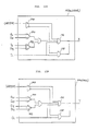
- the prior art AGC circuit generally 10, comprises a baseband variable attenuator (ATT) 12, a 4-bits analog-to-digital (AD) converter 14, an exclusive OR (Ex-OR) gate 16, and a low pass filter (LPF) 18.
- ATT baseband variable attenuator
- AD analog-to-digital
- Ex-OR exclusive OR
- LPF low pass filter
- An 8-bits baseband signal which is an input signal, is applied to the AD converter 14 via the ATT 12.
- the AD converter 14 regenerates main data signals Dl to D3, and an error signal D4.
- the signals D1 and D4 are routed to the Ex-OR gate 16 which then produces a signal C1.
- the signal C1 is fed as a control signal to the ATT 12 via the LPF 18 so as to control the input level of the AD converter 14 to an optimum one.
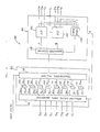
- a chart representative of the operation of the AGC circuit 10 is shown.
- the 8-levels baseband signal is designated by dl to d8 and the data outputted by the Ex-OR gate 16 by Cl.
- the input data dl to d8 are remote from the center, or zero volt, i. e. , when the demodulation level is increased, all the outputs Cl become logical ZEROs; when the demodulation level is decreased, the outputs Cl become ONEs.
- a false pull-in phenomenon will be described next. Assume that a modulated signal d'l to d'8 having a value which is 7/9 of a regular level is initially applied to the AD converter 14. In this condition, ZEROs and ONEs appear with the same probability on the output Cl of the Ex-OR gate 16, so the error signals nominally appear stable and the circuit 10 does not behave to restore the demodulated signal to the regular level. In this manner, once entered into d'I to d'8 as shown in Fig. 2, the demodulated signak cannot get out thereof, resulting in a false pull-in.
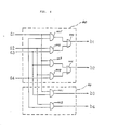
- the AGC circuit in accordance with one embodiment of the present invention is shown.
- the AGC circuit generally 20, includes an ATT 12, an AD converter 14 and a LPF 18 which share the same functions as those of the prior art AGC circuit 10.
- a subtractor 22 is interconnected between the ATT 12 and the AD converter 14, and a logic circuit 24 between the AD converter 14 and the ATT 12.
- a second logic circuit 26 is interconnected between the logic circuit 24 and the subtractor 22.
- the logic circuit 24 comprises an OR/NOR gates 28, 30, 32 and 34, AND gates 36 and 38, a selector 40, a flip-flop 42, and a LPF 18.
- the other logic circuit 26, on the other hand, comprises a selector 44, a flip-flop 46, and a LPF 48.
- a demodulated signal is routed through the ATT 12 and subtractor 22 to the AD converter 14 to be thereby converted to data sequences Dl to D4.
- the AD converter 14 produces signals Dl to D4 as shown on the righthand side in Fig. 2.
- the first logic circuit 24 is adapted to produce an error signal which is the characteristic feature of this particular embodiment As shown in Fig. 2, three different signal regions 1 to 3 are defined. When the demodulated signal has entered the signal regions 1 and 3, the logic circuit 24 controls the ATT 12 to reduce the demodulated signal.
- the logic circuit 24 delivers to the ATT 12 a control signal for magnifying the demodulated signal.
- This allows the demodulated signal to be stabilized in the regular state as shown in Fig. 2, in which dl contacts the region 1, d4 and d5 contacts the region 2, and d8 contacts the region 3.
- the demodulated signal d'l to d'8 has initially been applied to the AD converter 14, d'4 and d'5 enter the region 2 but not the regions 1 and 3.
- the demodulted signal is sequentially increased by the ATT 12 until d'l and d'8 respectively enter the regions 1 and 3 and, thereafter, they are stabilized at the points dl to d8.
- the circuit 20 with such a construction is free from false pull-in.
- a signal bl becomes a ONE in response to the regions 1 and 3 so as to reset the flip-flop 42 and, thereby, make an output of the flip-flop 42 a ZERO.
- a signal b2 becomes a ONE in response to the region 2 to set the flip-flop 42 to turn an output thereof into a ONE.
- a ONE be a positive voltage and a ZERO a negative voltage.
- the ATT 12 has such a characteristic that the amount of attenuation is decreased in response to a positive voltage and increased in response to a negative voltage, the above-stated operation is accomplished by applying an output of the flip-flop 42 to the ATT 12 via the LPF 18 which is adapted for jitter suppression.
- the second logic circuit 26 and the subtractor 22 in combination constitute a circuit for compensating for DC drifts as are contained in a demodulated signal on the input of the AD converter 14.
- a reference may be made to Japanese Unexamined Patent Publication No. 59-174058. It is to be noted that this DC voltage control circuit is not essential although preferable for more accurate operation of the AGC circuit 20.
- the reions 1 to 3 are shown in relation to an 8- levels demodulated signal; the region 1 contacting dl from outside, the region 2 contacting d4 and d5 from inside, and the reion 3 contacting d8 from outside.
- the number of levels is increased such as to sixteen levels, simply defining the regions 1 to 3 at the outermost points and innermost point excessively limits the number of signal points which are available for control.
- the increase in the number of levels may be coped with by defining several zones inclusive of the outermost and innermost points so as to increase the number of signals available for control while preserving the advantage of the present invention.
- the selector 40 is made up of AND gates 401 to 404 and OR gates 405 and 406.
- the selector 44 is made up of AND gates 441 and 442.
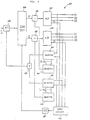
- FIG. 5 another embodiment of the present invention which is applied to a 64 QAM demodulator is shown.
- the AGC circuit shown in Fig. 5 and generally designated by the reference numeral 50 comprises an intermediate frequency (IF) band variable attenuator 52, a quadrature detector 54, subtractors 56 and 58, 4-bits AD converters 60 and 62, an adder 64, a logic circuit 66, a voltage controlled oscillator (VCO) 68, and selectors 40 and 44.
- a 64 QAM modulated wave is routed via the variable attenuator 52 to the quadrature detector 54 to be detected and thereby converted to 8-levels demodulated signals as represented by P and Q.
- variable attenuator 52 may be replaced with two such attenuators which are assigned one to the baseband of P and the other to that of Q. Further, one baseband variable attenuator and one IF band variable attenuator may be assigned to one of P and Q, as disclosed in Japanese Unexamined Patent Publication No. 59-169256.
- a reference carrier wave which is necessary for quadrature detection is regenerated by the logic circuit 66 and VCO 68. For details of such regeneration, a reference may be made to Japanese Unexamined Patent Publication 57-131151.
- the AGe circuit, generally 70 is substantially the same in construction and operation as the AGC circuit 50 of Fig. 5 except for a carrier asynchronism detection circuit 72 and logic circuits 74.
- the AGC circuit 70 is constructed to switch control signals from one to the other depending upon the steady/transitional state of the 64 QAM demodulator. Specifically, whether the demodulator is in a steady state or in a transitional state is determined by checking whether the carrier asynchronism detection circuit, or detector, 72 is in a synchronous state or in an asynchronous state.
- control signals in accordance with this embodiment are used in order to avoid false pull-in and, if it is in a steady state, prior art control signals.
- the advantage attainable with such a construction is that because in a steady state which is free from the possibility of false pull-in all the signals are used as control signals, use can be made of prior art control signals which have an excellent jitter characteristic.
- the number of signal points usable as control signals of the present invention decreases with the increase in the number of levels, preventing the jitter characteristic from being deteriorated.
- the carrier asynchronism detector 72 may be implemented with a detector of the type utilizing the fact that the loop impedance of a carrier synchronizing circuit is high under an asynchronous state and low under a synchronous state.
- the logic circuit 74 comprises an Ex-OR gate 76, AND gates 78 and 80, and OR gates 82 and 84.
- the output of the Ex-OR gate 76 is a prior art control signal while the output of the flip-flop 42 is a control signal in accordance with the present invention. The two outputs are switched from one to the other by a switching signal S.
- an AGC signal b5 is outputted when the output states of P and Q are in the signal regions 1 to 3 of Fig. 2.
- an arrangement may be made such that the control signal b5 is outputted only when the output states of P and Q enter the regions 1 to 3 at the same time.
- This alternative scheme is advantageous in that even in a transitional state of the demodulator the signals (dl, d4, d5 and d8) can be identified and regenerated in the same conditions as during a steady state, enhancing the pull-in characteristic during a transitional state.
- Figs. 3 and 5 have been shown and described in relation to an 8-levels baseband signal, such is only illustrative and they are naturally applicable to baseband signals having two or more levels.
- the equalizer 92 is made up of a weighting control signal generator 96, a transversal filter 98, adders 102, 104, 106 and 108, and subtractors 110, 112, 114 and 116.
- the demodulator 94 is made up of a quadrature detector 118, 3-bits AD converters 120 and 122, and a carrier regenerator 124.
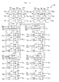
- An exemplary construction of the weighting control signal generator 96 is shown in Fig. 9. As shown in Fig.
- the generator 96 comprises 1-bit delay lines 126, 128, 130, 132, 134, 136, 138, 140, 142, 144, 146, 148, 150, 152, 154, 156, 158 and 160, region discriminators 162a, 162b, 164a and 164b, Ex-OR gates 166, 168, 170, 172, 174, 176, 178, 180, 182, 184, 186, 188, 190, 192, 194 and 196, and D-type flip-flops 198, 200, 202, 204, 206, 208, 210, 212, 214, 216, 218, 220, 222, 224, 226 and 228.
- FIG. 10 is a chart demonstrating the operation of this particular embodiment.
- Fig. 8 shows a demodulation system of the type using a 5-taps IF band transversal equalizer which is applicable to 16 QAM demodulated signals. Such a system will be described hereinafter.
- An input signal, or 16 QAM modulated wave, is applied to the transversal filter 98 which is made up of a delay circuit and a weighting circuit.
- the transversal filter 98 functions to compensate for intersymbol interference which is contained in the input signal.
- the basic operation of the transversal equalizer is disclosed in, for example, a paper entitled "Demodulator with 4/5 GHz 16 QAM 200 Mb/s Transversal Equalizer" which was presented at the 1984 National Meeting of Institute of Electronic Engineers, Communications Section, No. 628.
- the output of the transversal equalizer 92 is applied to the demodulator 94 and detected by the quadrature detector 118, thereby being turned into demodulated baseband signals P and Q.
- the baseband signals P and Q are converted to digital signals by the 3-bits AD converters 120 and 122, respectively.
- the AD converter 120 regenerates main signals D 1P and D 21 and an error signal Ep while the AD converter 122 regenerates main signals D 19 and D 29 and an error signal E 9 .
- the regenerated signals and the input signals are related as shown in Fig. 10.
- a, to a 16 are representative of the input signals, D 19 , D ; q and Eq the outputs of the AD converter 122, and D i p, D 2P and E.
- a reset signal R outputted by the carrier regenerator 124 is a signal adapted to show whether the regenerator 124 is in a synchronous state or in an asynchronous state and is applied to the weighting control signal generator 96.
- the weighting control signal generator 96 is one of characteristic features of the present invention and will be described in detail hereinafter.
- the construction shown in Fig. 9 includes region discriminators 162a, 162b, 164a and 164b and D-type flip-flops 198, 200, 202, 204, 206, 208, 210, 212, 214, 216, 218, 220, 222, 224, 226 and 228 which serve as storages, in addition to various elements as customarily built in.
- region discriminators 162a, 162b, 164a and 164b and D-type flip-flops 198, 200, 202, 204, 206, 208, 210, 212, 214, 216, 218, 220, 222, 224, 226 and 228 which serve as storages, in addition to various elements as customarily built in.
- a drawback particular to a prior art construction will be discussed.
- Fig. 10 assume that the signals as represented by a, to a t6 have intersymbol interference as represented by circles m 4 to ms, and that the demodulator
- the signals at to a 16 go round the circles m 1 to m 3 .
- the signals a 1 , as and a,3, for example, are shifted to a' 1 , a' s and a' 13 , respectively.
- the demodulator 94 is in a synchronous state, the signals a 1 , as and a l3 respectively remain in the positions a' 1 , a' 5 and a,3 and, in this condition, correct error signals are produced to promote convergence.
- the region discriminators 162a, 162b, 164a and 164b and the storages 198, 200, 202, 204, 206, 208, 210, 212, 214, 216, 218, 220, 222, 224, 226 and 228 as shown in Fig. 9 serve to eliminate the above-discussed malfunction.
- the region discriminators 162a and 162b are adapted to identify the outermost regions A and the innermost region A' on the diagonal as shown in Fig. 10.
- the region discriminators 162a and 162b respectively generate clock pulses when the signals a 1 to a 4 are subjected to interference of the same phase and the same polarity and when the signals a,3 to a 16 are subjected to interference of the same phase and the opposite polarity.
- Outputs of the Ex-OR gates 166, 168, 170, 172, 174, 176, 178 and 180 produced then are read by their associated flip-flops 198, 200, 202, 204, 206, 208, 210 and 212.
- the region discriminators 162a and 162b produce no output, the flip-flops mentioned above hold information previously stored therein.
- those flip-flops are capable of producing error signals from only those signals which entered the regions A and A'. Stated another way, because the flip-flop outputs do not contain incorrect error signals derived from the signals as to a t2 having middle levels as previously mentioned, correct error signals are constantly produced despite intersymbol interference of the degree as represented by circles m, to m 7 in Fig. 10.
- the region discriminators 164a and 164b are adapted to discriminate the regions A and regions B and B' which neighbor each of the regions A.
- the discriminators 164a and 164b generate clock pulses when signal points entered their associated regions.
- the signals Ip ⁇ 1, Ip ⁇ 2, Iq ⁇ 1 and Iq ⁇ 2 shown in Fig. 9 are derived from the signals a, to a,. So far as a control circuit associated with imaginary number portions is concerned, it unlike a control circuit associated with real number portions does not become unable to converge even if error signals derived from a prior art circuit construction are used. Nevertheless, as shown in Fig. 9, the use of region discriminators 164a and 164b is effective to reduce the probability of incorrectness of error signals and, thereby, speed up the convergence.
- the region discriminators 162a, 162b, 164a and 164b are furnished with a capability of restoring the function of a prior art control circuit when the demodulator 94 is in a normal state, i. e. , when the carrier regenerator 124 is in a synchronous state. Specifically, when the reset signal R has disappeared, clock pulses are continuously delivered as signals X and Y so as to make the flip-flops 198 to 228 through with the result that the same control signals as in a prior art circuit are produced.
- the advantage of the above-described construction is as follows.
- the region discriminators in this particular embodiment are capable of recovering the demodulation system even if the demodulator 94 is in an asynchronous state with input signals subjected to significant intersymbol interference.
- the number of signal points used as control signals is small; for example, in the case of 16 QAM system as shown in Fig. 10, only 1/4 of the signal points is used.
- the proportion of the signal points used sequentially decreases as the number of levels of input signals is increased. Because a decrease in the proportion of signal points used is reflected by an increase in jitter which is contained in control signals, it is preferable that while the demodulator is normal, use is made of the prior art construction which prepares control signals using all the signals.
- the region discriminators operate nominally with the same construction as the prior art ones so long as the demodulator is in a normal state, as previously stated.
- the region discriminator 162a (162b) comprises Ex-OR gates 130 and 132, an OR/NOR gate 134, and AND gates 136 and 138.
- the region discriminator 164a (164b) comprises Ex-OR gates 140 and 142, -an OR/NOR gate 144, and AND gates 146 and 148. Because the construction of each region discriminator is relatively simple, detailed description thereof will be omitted.
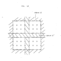
- Fig. 12 there is shown one example of discrimination regions which are associated with a real number portion control circuit for 64 QAM modulated waves. As shown, there are defined a signal region A which contacts the maximum level signals of demodulated signals P and Q from outside and a region A' which contacts the minimum level signals from inside. In this case, the regions are defined for each of P and Q. In, this manner, the regions A and A' are adequately set up in matching relation to the number of levels and the arrangement of signal points.
- Fig. 8 While in Fig. 8 the transversal equalizer has been shown in relation to the IF band, use may be made of a baseband transversal equalizer, in which case the outputs of the weighting control signal generator will be directly applied to P and Q baseband transversal filters. Where this embodiment is applied to a high multi-level modulation wave having sixteen or more levels; what is required is simply increasing the number of bits of the AD converters 120 and 122 of Fig. 8 and modifying the regions to be discriminated by the discriminators 162a, 162b, 164a and 164b of Fig. 9. Further, the 5-taps transversal equalizer shown and described is only illustrative and may be replaced with another.
- the digital demodulation system is capable of being restored to normal even if a demodulator is in an asynchronous state and input signals involve significant intersymbol interference.
- This allows a transversal equalizer included in the system to fully exhibit an equalizing function thereof.
Priority Applications (1)
| Application Number | Priority Date | Filing Date | Title |
|---|---|---|---|
| EP92103182A EP0486474B1 (fr) | 1985-06-29 | 1986-06-27 | Procédé d'adaptation d'un égaliseur transversal, sans synchronisation de la porteuse |
Applications Claiming Priority (4)
| Application Number | Priority Date | Filing Date | Title |
|---|---|---|---|
| JP141529/85 | 1985-06-29 | ||
| JP60141529A JPH0797746B2 (ja) | 1985-06-29 | 1985-06-29 | 自動利得制御回路 |
| JP149931/85 | 1985-07-10 | ||
| JP60149931A JPH0697755B2 (ja) | 1985-07-10 | 1985-07-10 | デイジタル復調システム |
Related Child Applications (1)
| Application Number | Title | Priority Date | Filing Date |
|---|---|---|---|
| EP92103182.9 Division-Into | 1992-02-25 |
Publications (3)
| Publication Number | Publication Date |
|---|---|
| EP0213309A2 true EP0213309A2 (fr) | 1987-03-11 |
| EP0213309A3 EP0213309A3 (en) | 1989-04-05 |
| EP0213309B1 EP0213309B1 (fr) | 1994-01-05 |
Family
ID=26473745
Family Applications (2)
| Application Number | Title | Priority Date | Filing Date |
|---|---|---|---|
| EP86108803A Expired - Lifetime EP0213309B1 (fr) | 1985-06-29 | 1986-06-27 | Circuit de contrôle automatique de gain |
| EP92103182A Expired - Lifetime EP0486474B1 (fr) | 1985-06-29 | 1986-06-27 | Procédé d'adaptation d'un égaliseur transversal, sans synchronisation de la porteuse |
Family Applications After (1)
| Application Number | Title | Priority Date | Filing Date |
|---|---|---|---|
| EP92103182A Expired - Lifetime EP0486474B1 (fr) | 1985-06-29 | 1986-06-27 | Procédé d'adaptation d'un égaliseur transversal, sans synchronisation de la porteuse |
Country Status (5)
| Country | Link |
|---|---|
| US (1) | US4703282A (fr) |
| EP (2) | EP0213309B1 (fr) |
| AU (1) | AU579554B2 (fr) |
| CA (2) | CA1282127C (fr) |
| DE (2) | DE3650568T2 (fr) |
Cited By (20)
| Publication number | Priority date | Publication date | Assignee | Title |
|---|---|---|---|---|
| EP0252500A2 (fr) * | 1986-07-09 | 1988-01-13 | Nec Corporation | Démodulateur de modulation à déplacement de phase à 8 états |
| EP0262644A2 (fr) * | 1986-09-30 | 1988-04-06 | Nec Corporation | Démodulateur QAM à fonction de resynchronisation rapide |
| EP0281308A2 (fr) * | 1987-03-02 | 1988-09-07 | AT&T Corp. | Circuit de contrôle commandé par la décision et procédé d'ajustement d'appareils commandés par la décision |
| EP0308891A2 (fr) * | 1987-09-21 | 1989-03-29 | Nec Corporation | Démodulateur de QAM en escalier utilisant tous les points du signal pour générer des signaux de commande |
| EP0465851A2 (fr) * | 1990-06-14 | 1992-01-15 | Oy Nokia Ab | Récepteur de signaux MAQ qui compense à la fois des distorsions linéaires et non-linéaires |
| EP0501448A2 (fr) * | 1991-02-27 | 1992-09-02 | Nec Corporation | Circuit de commande de gain pour démodulateur MAQ |
| FR2688367A1 (fr) * | 1993-03-01 | 1993-09-10 | Alcatel Nv | Commande de gain automatique dans un recepteur radioelectrique comportant un circuit d'egaliseur temporel. |
| GB2288107A (en) * | 1994-03-18 | 1995-10-04 | Fujitsu Ltd | Quadrature amplitude modulation receiver |
| GB2323505A (en) * | 1994-03-18 | 1998-09-23 | Fujitsu Ltd | Quadrature amplitude modulation receiver |
| EP1862779A2 (fr) | 2006-05-30 | 2007-12-05 | Fujitsu Ltd. | Système et procédé pour régler de manière non linéaire une compensation de décalage appliquée à un signal |
| EP1862766A3 (fr) * | 2006-05-30 | 2008-04-09 | Fujitsu Ltd. | Système et procédé pour régler asymétriquement une compensation appliquée à un signal |
| US7760798B2 (en) | 2006-05-30 | 2010-07-20 | Fujitsu Limited | System and method for adjusting compensation applied to a signal |
| US7764757B2 (en) | 2006-05-30 | 2010-07-27 | Fujitsu Limited | System and method for the adjustment of offset compensation applied to a signal |
| US7787534B2 (en) | 2006-05-30 | 2010-08-31 | Fujitsu Limited | System and method for adjusting offset compensation applied to a signal |
| US7801208B2 (en) | 2006-05-30 | 2010-09-21 | Fujitsu Limited | System and method for adjusting compensation applied to a signal using filter patterns |
| US7804921B2 (en) | 2006-05-30 | 2010-09-28 | Fujitsu Limited | System and method for decoupling multiple control loops |
| US7804894B2 (en) | 2006-05-30 | 2010-09-28 | Fujitsu Limited | System and method for the adjustment of compensation applied to a signal using filter patterns |
| US7817757B2 (en) | 2006-05-30 | 2010-10-19 | Fujitsu Limited | System and method for independently adjusting multiple offset compensations applied to a signal |
| US7817712B2 (en) | 2006-05-30 | 2010-10-19 | Fujitsu Limited | System and method for independently adjusting multiple compensations applied to a signal |
| US7839958B2 (en) | 2006-05-30 | 2010-11-23 | Fujitsu Limited | System and method for the adjustment of compensation applied to a signal |
Families Citing this family (10)
| Publication number | Priority date | Publication date | Assignee | Title |
|---|---|---|---|---|
| JPS62298255A (ja) * | 1986-06-18 | 1987-12-25 | Fujitsu Ltd | 識別装置 |
| US4995106A (en) * | 1989-08-24 | 1991-02-19 | Ampex Corporation | Fast decision feedback decoder for digital data |
| US5097486A (en) * | 1990-07-31 | 1992-03-17 | Ampex Corporation | Pipelined decision feedback decoder |
| AU673390B2 (en) * | 1993-01-20 | 1996-11-07 | Nec Corporation | An AGC circuit for burst signal |
| US5828692A (en) * | 1995-12-06 | 1998-10-27 | Rockwell International Corporation | Baseband demodulator for polar or rectangular modulated signal in a cordless spread spectrum telephone |
| KR100241890B1 (ko) | 1997-01-10 | 2000-03-02 | 윤종용 | 디지털 통신 시스템에서 간섭 제거 회로 |
| US6546063B1 (en) | 1998-02-10 | 2003-04-08 | Agere Systems Inc. | Asynchronous clock for adaptive equalization |
| US6038266A (en) * | 1998-09-30 | 2000-03-14 | Lucent Technologies, Inc. | Mixed mode adaptive analog receive architecture for data communications |
| US6680985B1 (en) * | 2000-08-15 | 2004-01-20 | Hughes Electronics Corporation | Adaptive quadrature amplitude modulation decoding system |
| JP3594297B2 (ja) * | 2000-11-08 | 2004-11-24 | 株式会社日立国際電気 | データ再生方式およびデータ再生器 |
Citations (1)
| Publication number | Priority date | Publication date | Assignee | Title |
|---|---|---|---|---|
| EP0120474A2 (fr) * | 1983-03-23 | 1984-10-03 | Nec Corporation | Circuits de commande de tension continue |
Family Cites Families (10)
| Publication number | Priority date | Publication date | Assignee | Title |
|---|---|---|---|---|
| US4283682A (en) * | 1979-04-06 | 1981-08-11 | Ricoh Company, Ltd. | Erasure zone decision feedback phase lock loop for carrier recovery in data modems |
| JPS5615775A (en) | 1979-07-18 | 1981-02-16 | Hideaki Sasaki | Ball safe device for pinball machine |
| JPS57131151A (en) | 1981-02-06 | 1982-08-13 | Nec Corp | Carrier wave reproducing circuit |
| JPS5962228A (ja) | 1982-10-01 | 1984-04-09 | Nec Corp | 自動等化器 |
| JPH063947B2 (ja) * | 1983-03-16 | 1994-01-12 | 日本電気株式会社 | 自動利得制御回路 |
| JPS59174058A (ja) | 1983-03-23 | 1984-10-02 | Nec Corp | 直流電圧制御回路 |
| US4602374A (en) * | 1984-02-27 | 1986-07-22 | Nippon Telegraph & Telephone Public Corporation | Multi-level decision circuit |
| JPS6156555A (ja) * | 1984-08-27 | 1986-03-22 | Nec Corp | 復調装置 |
| JPS61112414A (ja) * | 1984-11-06 | 1986-05-30 | Nec Corp | 自動レベル制御回路 |
| JPS61137446A (ja) * | 1984-12-10 | 1986-06-25 | Nec Corp | 復調装置 |
-
1986
- 1986-06-26 CA CA000512494A patent/CA1282127C/fr not_active Expired - Lifetime
- 1986-06-26 US US06/878,746 patent/US4703282A/en not_active Expired - Lifetime
- 1986-06-27 EP EP86108803A patent/EP0213309B1/fr not_active Expired - Lifetime
- 1986-06-27 DE DE3650568T patent/DE3650568T2/de not_active Expired - Lifetime
- 1986-06-27 DE DE86108803T patent/DE3689499T2/de not_active Expired - Lifetime
- 1986-06-27 AU AU59337/86A patent/AU579554B2/en not_active Expired
- 1986-06-27 EP EP92103182A patent/EP0486474B1/fr not_active Expired - Lifetime
-
1990
- 1990-10-09 CA CA000615890A patent/CA1292525C/fr not_active Expired - Lifetime
Patent Citations (1)
| Publication number | Priority date | Publication date | Assignee | Title |
|---|---|---|---|---|
| EP0120474A2 (fr) * | 1983-03-23 | 1984-10-03 | Nec Corporation | Circuits de commande de tension continue |
Cited By (33)
| Publication number | Priority date | Publication date | Assignee | Title |
|---|---|---|---|---|
| EP0252500A3 (en) * | 1986-07-09 | 1989-11-23 | Nec Corporation | 8-phase phase-shift keying demodulator |
| EP0252500A2 (fr) * | 1986-07-09 | 1988-01-13 | Nec Corporation | Démodulateur de modulation à déplacement de phase à 8 états |
| EP0262644A3 (en) * | 1986-09-30 | 1988-11-30 | Nec Corporation | Qam demodulator with rapid resynchronization function |
| EP0262644A2 (fr) * | 1986-09-30 | 1988-04-06 | Nec Corporation | Démodulateur QAM à fonction de resynchronisation rapide |
| JPS63228826A (ja) * | 1987-03-02 | 1988-09-22 | アメリカン テレフォン アンド テレグラフ カムパニー | 決定指令制御装置とその調節方法 |
| EP0281308A2 (fr) * | 1987-03-02 | 1988-09-07 | AT&T Corp. | Circuit de contrôle commandé par la décision et procédé d'ajustement d'appareils commandés par la décision |
| EP0281308A3 (en) * | 1987-03-02 | 1990-03-28 | American Telephone And Telegraph Company | Decision-directed control circuit |
| EP0308891A2 (fr) * | 1987-09-21 | 1989-03-29 | Nec Corporation | Démodulateur de QAM en escalier utilisant tous les points du signal pour générer des signaux de commande |
| EP0308891A3 (en) * | 1987-09-21 | 1990-08-29 | Nec Corporation | Stepped square-qam demodulator utilizing all signal points to generate control signals |
| EP0465851A2 (fr) * | 1990-06-14 | 1992-01-15 | Oy Nokia Ab | Récepteur de signaux MAQ qui compense à la fois des distorsions linéaires et non-linéaires |
| EP0465851A3 (en) * | 1990-06-14 | 1992-08-19 | Oy Nokia Ab | Qam receiver compensating both linear and non-linear distortion |
| EP0501448A2 (fr) * | 1991-02-27 | 1992-09-02 | Nec Corporation | Circuit de commande de gain pour démodulateur MAQ |
| EP0501448A3 (en) * | 1991-02-27 | 1993-04-14 | Nec Corporation | Gain control circuitry for qam demodulator |
| FR2688367A1 (fr) * | 1993-03-01 | 1993-09-10 | Alcatel Nv | Commande de gain automatique dans un recepteur radioelectrique comportant un circuit d'egaliseur temporel. |
| GB2323505A (en) * | 1994-03-18 | 1998-09-23 | Fujitsu Ltd | Quadrature amplitude modulation receiver |
| US5596605A (en) * | 1994-03-18 | 1997-01-21 | Fujitsu Limited | Radio receiver for use in the reception of digital multiplexing signals |
| GB2288107A (en) * | 1994-03-18 | 1995-10-04 | Fujitsu Ltd | Quadrature amplitude modulation receiver |
| GB2288107B (en) * | 1994-03-18 | 1998-11-04 | Fujitsu Ltd | Radio receiver for use in the reception of digital multiplexing signals |
| GB2323505B (en) * | 1994-03-18 | 1998-11-04 | Fujitsu Ltd | Radio receiver for use in the reception of digital multiplexing signals |
| US7764757B2 (en) | 2006-05-30 | 2010-07-27 | Fujitsu Limited | System and method for the adjustment of offset compensation applied to a signal |
| US7804921B2 (en) | 2006-05-30 | 2010-09-28 | Fujitsu Limited | System and method for decoupling multiple control loops |
| EP1862779A3 (fr) * | 2006-05-30 | 2008-04-09 | Fujitsu Ltd. | Système et procédé pour régler de manière non linéaire une compensation de décalage appliquée à un signal |
| US7760798B2 (en) | 2006-05-30 | 2010-07-20 | Fujitsu Limited | System and method for adjusting compensation applied to a signal |
| EP1862779A2 (fr) | 2006-05-30 | 2007-12-05 | Fujitsu Ltd. | Système et procédé pour régler de manière non linéaire une compensation de décalage appliquée à un signal |
| US7787534B2 (en) | 2006-05-30 | 2010-08-31 | Fujitsu Limited | System and method for adjusting offset compensation applied to a signal |
| US7801208B2 (en) | 2006-05-30 | 2010-09-21 | Fujitsu Limited | System and method for adjusting compensation applied to a signal using filter patterns |
| EP1862766A3 (fr) * | 2006-05-30 | 2008-04-09 | Fujitsu Ltd. | Système et procédé pour régler asymétriquement une compensation appliquée à un signal |
| US7804894B2 (en) | 2006-05-30 | 2010-09-28 | Fujitsu Limited | System and method for the adjustment of compensation applied to a signal using filter patterns |
| US7817757B2 (en) | 2006-05-30 | 2010-10-19 | Fujitsu Limited | System and method for independently adjusting multiple offset compensations applied to a signal |
| US7817712B2 (en) | 2006-05-30 | 2010-10-19 | Fujitsu Limited | System and method for independently adjusting multiple compensations applied to a signal |
| US7839955B2 (en) | 2006-05-30 | 2010-11-23 | Fujitsu Limited | System and method for the non-linear adjustment of compensation applied to a signal |
| US7839958B2 (en) | 2006-05-30 | 2010-11-23 | Fujitsu Limited | System and method for the adjustment of compensation applied to a signal |
| US7848470B2 (en) | 2006-05-30 | 2010-12-07 | Fujitsu Limited | System and method for asymmetrically adjusting compensation applied to a signal |
Also Published As
| Publication number | Publication date |
|---|---|
| AU579554B2 (en) | 1988-11-24 |
| EP0486474A2 (fr) | 1992-05-20 |
| DE3689499T2 (de) | 1994-04-28 |
| US4703282A (en) | 1987-10-27 |
| EP0213309A3 (en) | 1989-04-05 |
| EP0486474B1 (fr) | 1996-09-11 |
| EP0213309B1 (fr) | 1994-01-05 |
| EP0486474A3 (en) | 1992-08-12 |
| DE3650568T2 (de) | 1997-04-30 |
| AU5933786A (en) | 1987-01-08 |
| DE3650568D1 (de) | 1996-10-17 |
| CA1282127C (fr) | 1991-03-26 |
| CA1292525C (fr) | 1991-11-26 |
| DE3689499D1 (de) | 1994-02-17 |
Similar Documents
| Publication | Publication Date | Title |
|---|---|---|
| US4703282A (en) | Digital demodulation system | |
| EP0120416B1 (fr) | Démodulateur comportant un circuit de commande automatique de gain | |
| US4458356A (en) | Carrier recovery circuit | |
| CA1224542A (fr) | Demodulation pour systeme de modulation d'amplitude multiniveau | |
| JPH02131031A (ja) | 復調装置 | |
| EP0118119B1 (fr) | Circuit de synchronisation d'horloge | |
| EP0120474B1 (fr) | Circuits de commande de tension continue | |
| JPS6387828A (ja) | デイジタル復調システム | |
| US4466109A (en) | Carrier recovery arrangement for sixteen-state amplitude and phase modulation and receiving system for digital data, comprising such an arrangement | |
| EP0212582B1 (fr) | Système de démodulation capable d'établir une synchronisation dans un état transitoire | |
| US4803438A (en) | 8-phase phase-shift keying demodulator | |
| US4631488A (en) | QAM demodulator with distortion compensation | |
| CA1206215A (fr) | Dispositif de demodulation pour ondes modulees psk-psk composites | |
| JP2534650B2 (ja) | 復調装置 | |
| JP2560339B2 (ja) | ディジタル復調装置 | |
| JP2564840B2 (ja) | ディジタル復調装置 | |
| JPH0515336B2 (fr) | ||
| JP2526540B2 (ja) | 搬送波同期回路 | |
| JP2871172B2 (ja) | 復調装置 | |
| JPH0712178B2 (ja) | デイジタル変復調システム | |
| JPS6239923A (ja) | 復調システム | |
| JPH0797746B2 (ja) | 自動利得制御回路 | |
| JP2540958B2 (ja) | ディジタル変復調システム | |
| JPS6239922A (ja) | デイジタル復調システム | |
| JPH0697755B2 (ja) | デイジタル復調システム |
Legal Events
| Date | Code | Title | Description |
|---|---|---|---|
| PUAI | Public reference made under article 153(3) epc to a published international application that has entered the european phase |
Free format text: ORIGINAL CODE: 0009012 |
|
| 17P | Request for examination filed |
Effective date: 19860627 |
|
| AK | Designated contracting states |
Kind code of ref document: A2 Designated state(s): DE FR GB IT NL SE |
|
| PUAL | Search report despatched |
Free format text: ORIGINAL CODE: 0009013 |
|
| AK | Designated contracting states |
Kind code of ref document: A3 Designated state(s): DE FR GB IT NL SE |
|
| 17Q | First examination report despatched |
Effective date: 19910424 |
|
| RTI1 | Title (correction) | ||
| GRAA | (expected) grant |
Free format text: ORIGINAL CODE: 0009210 |
|
| AK | Designated contracting states |
Kind code of ref document: B1 Designated state(s): DE FR GB IT NL SE |
|
| PG25 | Lapsed in a contracting state [announced via postgrant information from national office to epo] |
Ref country code: IT Free format text: LAPSE BECAUSE OF FAILURE TO SUBMIT A TRANSLATION OF THE DESCRIPTION OR TO PAY THE FEE WITHIN THE PRE;WARNING: LAPSES OF ITALIAN PATENTS WITH EFFECTIVE DATE BEFORE 2007 MAY HAVE OCCURRED AT ANY TIME BEFORE 2007. THE CORRECT EFFECTIVE DATE MAY BE DIFFERENT FROM THE ONE RECORDED.SCRIBED TIME-LIMIT Effective date: 19940105 Ref country code: NL Effective date: 19940105 Ref country code: SE Effective date: 19940105 Ref country code: FR Effective date: 19940105 |
|
| XX | Miscellaneous (additional remarks) |
Free format text: TEILANMELDUNG 92103182.9 EINGEREICHT AM 27/06/86. |
|
| REF | Corresponds to: |
Ref document number: 3689499 Country of ref document: DE Date of ref document: 19940217 |
|
| EN | Fr: translation not filed | ||
| NLV1 | Nl: lapsed or annulled due to failure to fulfill the requirements of art. 29p and 29m of the patents act | ||
| PLBE | No opposition filed within time limit |
Free format text: ORIGINAL CODE: 0009261 |
|
| STAA | Information on the status of an ep patent application or granted ep patent |
Free format text: STATUS: NO OPPOSITION FILED WITHIN TIME LIMIT |
|
| 26N | No opposition filed | ||
| REG | Reference to a national code |
Ref country code: GB Ref legal event code: IF02 |
|
| PGFP | Annual fee paid to national office [announced via postgrant information from national office to epo] |
Ref country code: GB Payment date: 20050622 Year of fee payment: 20 |
|
| PGFP | Annual fee paid to national office [announced via postgrant information from national office to epo] |
Ref country code: DE Payment date: 20050623 Year of fee payment: 20 |
|
| REG | Reference to a national code |
Ref country code: GB Ref legal event code: PE20 |
|
| PG25 | Lapsed in a contracting state [announced via postgrant information from national office to epo] |
Ref country code: GB Free format text: LAPSE BECAUSE OF EXPIRATION OF PROTECTION Effective date: 20060626 |