EP0202746B1 - Elément métallique ayant une surface traitée, procédé de préparation et utilisation comme élément photoconducteur - Google Patents
Elément métallique ayant une surface traitée, procédé de préparation et utilisation comme élément photoconducteur Download PDFInfo
- Publication number
- EP0202746B1 EP0202746B1 EP86302519A EP86302519A EP0202746B1 EP 0202746 B1 EP0202746 B1 EP 0202746B1 EP 86302519 A EP86302519 A EP 86302519A EP 86302519 A EP86302519 A EP 86302519A EP 0202746 B1 EP0202746 B1 EP 0202746B1
- Authority
- EP
- European Patent Office
- Prior art keywords
- metal support
- support according
- less
- aluminum alloy
- photoconductive
- Prior art date
- Legal status (The legal status is an assumption and is not a legal conclusion. Google has not performed a legal analysis and makes no representation as to the accuracy of the status listed.)
- Expired - Lifetime
Links
Images


Classifications
-
- B—PERFORMING OPERATIONS; TRANSPORTING
- B24—GRINDING; POLISHING
- B24C—ABRASIVE OR RELATED BLASTING WITH PARTICULATE MATERIAL
- B24C1/00—Methods for use of abrasive blasting for producing particular effects; Use of auxiliary equipment in connection with such methods
- B24C1/06—Methods for use of abrasive blasting for producing particular effects; Use of auxiliary equipment in connection with such methods for producing matt surfaces, e.g. on plastic materials, on glass
-
- B—PERFORMING OPERATIONS; TRANSPORTING
- B24—GRINDING; POLISHING
- B24C—ABRASIVE OR RELATED BLASTING WITH PARTICULATE MATERIAL
- B24C11/00—Selection of abrasive materials or additives for abrasive blasts
-
- G—PHYSICS
- G03—PHOTOGRAPHY; CINEMATOGRAPHY; ANALOGOUS TECHNIQUES USING WAVES OTHER THAN OPTICAL WAVES; ELECTROGRAPHY; HOLOGRAPHY
- G03G—ELECTROGRAPHY; ELECTROPHOTOGRAPHY; MAGNETOGRAPHY
- G03G5/00—Recording-members for original recording by exposure, e.g. to light, to heat or to electrons; Manufacture thereof; Selection of materials therefor
- G03G5/10—Bases for charge-receiving or other layers
-
- Y—GENERAL TAGGING OF NEW TECHNOLOGICAL DEVELOPMENTS; GENERAL TAGGING OF CROSS-SECTIONAL TECHNOLOGIES SPANNING OVER SEVERAL SECTIONS OF THE IPC; TECHNICAL SUBJECTS COVERED BY FORMER USPC CROSS-REFERENCE ART COLLECTIONS [XRACs] AND DIGESTS
- Y10—TECHNICAL SUBJECTS COVERED BY FORMER USPC
- Y10S—TECHNICAL SUBJECTS COVERED BY FORMER USPC CROSS-REFERENCE ART COLLECTIONS [XRACs] AND DIGESTS
- Y10S428/00—Stock material or miscellaneous articles
- Y10S428/922—Static electricity metal bleed-off metallic stock
- Y10S428/923—Physical dimension
- Y10S428/924—Composite
- Y10S428/925—Relative dimension specified
-
- Y—GENERAL TAGGING OF NEW TECHNOLOGICAL DEVELOPMENTS; GENERAL TAGGING OF CROSS-SECTIONAL TECHNOLOGIES SPANNING OVER SEVERAL SECTIONS OF THE IPC; TECHNICAL SUBJECTS COVERED BY FORMER USPC CROSS-REFERENCE ART COLLECTIONS [XRACs] AND DIGESTS
- Y10—TECHNICAL SUBJECTS COVERED BY FORMER USPC
- Y10T—TECHNICAL SUBJECTS COVERED BY FORMER US CLASSIFICATION
- Y10T428/00—Stock material or miscellaneous articles
- Y10T428/12—All metal or with adjacent metals
- Y10T428/12389—All metal or with adjacent metals having variation in thickness
-
- Y—GENERAL TAGGING OF NEW TECHNOLOGICAL DEVELOPMENTS; GENERAL TAGGING OF CROSS-SECTIONAL TECHNOLOGIES SPANNING OVER SEVERAL SECTIONS OF THE IPC; TECHNICAL SUBJECTS COVERED BY FORMER USPC CROSS-REFERENCE ART COLLECTIONS [XRACs] AND DIGESTS
- Y10—TECHNICAL SUBJECTS COVERED BY FORMER USPC
- Y10T—TECHNICAL SUBJECTS COVERED BY FORMER US CLASSIFICATION
- Y10T428/00—Stock material or miscellaneous articles
- Y10T428/12—All metal or with adjacent metals
- Y10T428/12993—Surface feature [e.g., rough, mirror]
Definitions
- This invention relates to a surface treated metal support for a photoconductive layer for use in electrophotography.
- Known supports for photoconductive layers may be shaped as a plate, a cylinder or an endless belt etc and fabricated with a metal surface.
- the surface is often finished with a predetermined shape to prevent the generation of interference fringes and said surface may be machined by diamond cutting, or milling etc.
- cutting may be impaired by the presence of surface defects, possibly caused by the presence of intervening matter used in the production of the alloy forming the support.
- intervening matter used in the production of the alloy forming the support.
- hard intervening matter may exist in the aluminum structure, such as compounds of Si-Al-Fe, Fe-Al or TiB2, etc, along with oxides of aluminum, magnesium, titanium, silicon and iron.
- blisters may be produced due to the presence of hydrogen and defects may also occur due to grain boundaries.
- Cutting operations may also introduce other problems. Inconsistences in the surface may be introduced due to the presence of cutting powder and cutting oil, therefore further steps must be taken to remove these waste materials.
- amorphous silicon having its free bonds modified with monovalent elements such as hydrogen or halogens hereinafter referred to as a-Si(H,X) is a preferred material for the production of a photoconductive layer, due to its excellent photoconductivity, frictional resistance and heat resistance.
- a-Si(H,X) is fabricated from multiple layers.
- the uniformity on the photoconductive support is very important and, if there exist nonuniformity, the overall device may be rendered practically useless. It is known that the form of the a-Si(H,X) film is influenced greatly by the surface shape of the support. Above all, in an electrophotographic photosensitive drum, having a large area for which substantially uniform photoconductive characteristics are required, the surface condition of the support is very important and it should not include pillar-shaped structures or spherical projections.
- the electrophotographic photosensitive members receive sliding friction repeatedly with a blade or fur brush etc for the removal of residual toner.
- Durability of the photosensitive member to this operation may be improved by increasing the hardness of the support and increasing the abrasion resistance of the surface of the photoconductive layer.
- a very hard aluminum material is disclosed in Japanese Laid Open Patent Application No. 111046/1981.
- the use of an alloy having a high concentration of silicon tends to cause the silicon to precipitate from the alloy.
- a surface treated metal support for a photoconductive layer for use in electrophotography characterised in that a surface of said support has a plurality of spherical impressions distributed over the surface in such a way that their perimeters are in contact, wherein the radius of curvature R and the width D of the spherical impressions have values such that D divided by R is greater than or equal to 0.035 (0.35 ⁇ D/R ) and D is smaller than or equal to ⁇ 500 micrometer.
- the metal support is marked with impressions having substantially the same radius of curvature and width.
- Said support may be fabricated from an aluminum alloy and said alloy may, for example, comprise aluminum with crystal grains having a maximum size of 300 micrometer.
- An application of the surface treated metal support is in an electophotographic device, comprising a photoconductive layer on the metal support, with means for applying photo-radiation to the photoconductive layer, wherein the means for applying radiation is a laser giving rise to radiation having a spot diameter, such that the width D of the spherical impressions is less than that of the spot diameter.
- the width D of the marks may be 200 micrometer or less and is preferably 100 micrometer or less.
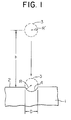
- the surface treated metal support 1 of the present invention comprises a plurality of spherical impressions 4 formed on the surface 2.
- rigid body true spheres 3 are permitted to free-fall from a position at a certain height from the surface 2, so as to collide against the surface 2 to form spherical mark impressions 4.
- a plurality of spherical mark impressions 4 with substantially the same radius of curvature R and the same width D can be formed on the surface 2.
- Fig. 2 and Fig. 3 show examples of the mark impressions formed in such cases.
- unevenness is formed by permitting a plurality of spherical bodies 3', 3,... with substantially the same diameter to fall from substantially the same height onto the surface 2' at different positions on the metal member 1', thereby forming a plurality of impressions 4', 4'... with substantially the same radius of curvature and width sparsely so that they may not be overlapped with each other.
- the height of unevenness is made smaller than the example shown in Fig. 1 by forming a plurality of impressions 4'', 4''... with substantially the same radius of curvature and width densely so that they may be overlapped with each other by permitting a plurality of spherical bodies with substantially the same diameter 3'', 3''... onto the positions on the surface 2'' of the metal member 1''.
- unevenness with irregular height is formed on the surface by permitting spherical bodies 3''', 3'''... with several kinds of diameters different from each other to fall from substantially the same height or different heights to form a plurality of impressions 4''', 4'''... with different radius of curvature and widths different from each other so that they may be overlapped with each other.
- a plurality of spherical mark impressions with desired radius of curvature and width can be formed at a desired density on the surface of a metal member by controlling suitably the conditions such as hardnesses of the rigid body true sphere and the surface of the metal member, the radius of the rigid body true sphere, the falling height, the amount of spheres fallen, etc. Accordingly, it is possible to control freely the surface coarseness, namely the height or the pitch of unevenness such as finishing of the metal member surface to a mirror surface or a non-mirror surface by selection of the above conditions, and it is also possible to form unevenness of a desired shape depending on the purpose of use.
- the bad surface condition of a port hole tube or a mandrel extrusion drawn Al tube can be corrected by use of the method of the present invention to be finished to a desired surface condition. This is due to plastic deformation of the irregular unevenness of the surface by collision of rigid body true spheres.
- the base material for the surface treated metal member of the present invention may be any kind of metals depending on the purpose of use, but it is practically aluminum and aluminum alloys, stainless steels, steel irons, copper and copper alloys, and magnesium alloys.
- the shape of the metal member may be selected as desired.
- the substrate (support) for electrophotographic photosensitive member shapes such as plates, cylinders, columns, endless belts, etc., may be practically used.
- the spherical bodies to be used in the present invention there by be used, for example, various rigid body spheres made of metals such as stainless steel, aluminum, steel irons, nickel, brass, etc., ceramics, plastics, etc.
- rigid body spheres made of stainless steel or steel irons are preferred for the reasons of durability and low cost.
- the hardness of the spherical bodies may be either higher or lower than the hardness of the metal member, but it is preferably higher than the hardness of the metal member when the spherical bodies are used repeatedly.
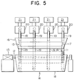
- Drawing working is applied optionally with treatment such as heat treatment or tempering, and the cylinder is worked by practicing the method of the present invention by using, for example, a device with the constitution as shown in Fig. 5 (front view) and Fig. 6 (longitudinal sectional view) to prepare a support.
- 11 is, for example, an aluminum cylinder for preparation of a support.
- the surface of the cylinder 11 may be previously finished to a suitable flatness.
- the cylinder 11 is supported axially on a rotatory shaft 12, driven by a suitable driving means 13 such as a motor and is made rotatable substantially around the shaft core.
- the rotation speed is determined and controlled in view of the density of the spherical mark impressions formed and the amount of the rigid body true spheres supplied, etc.
- a device for permitting the rigid body true spheres (balls) 15 to free-fall and it is constituted of a ball feeder 16 for storing and permitting the rigid body true spheres 15 to fall, a vibrator 17 for rocking the rigid body true spheres 15 so that they can fall readily from the feeder 16, a recovery tank 18 for recovering the rigid body true spheres 15 after collision against the cylinder 11, a ball delivering device 19 for transporting the rigid body true spheres recovered in the recovery tank 18 through a pipe to the feeder 16, a washing device 20 for liquid washing the rigid body true spheres 15 in the course of the delivering device 19, a reservoir 21 for supplying a washing liquid (solvent, etc.) through a nozzle, etc., to the washing device 20, and a recovery tank 22 for recovering the liquid used for washing.
- a ball feeder 16 for storing and permitting the rigid body true spheres 15 to fall
- a vibrator 17 for rocking the rigid body true spheres 15 so that they can fall readily from the feeder
- a recovery tank 18
- the amount of the rigid body true spheres free-falling from the feeder 16 may be controlled suitably by the degree of opening of the dropping port 23, the extent of rocking by means of the vibrator 17, etc.
- Such a photoconductive member is constructed by providing a photosensitive layer containing, for example, an organic photoconductive material or an inorganic photoconductive material on a support.
- the shape of the support may be determined as desired, but, for example, when it is to be used for electrophotography it should be shaped in an endless belt or a cylinder as described above in the case of continuous high speed copying.
- the thickness of the support may be determined suitably so that a photoconductive member as desired may be formed, but when flexibility as the photoconductive member is demanded, it is made as thin as possible within the range so far as the function of a support can be fully exhibited. However, even in such a case, for preparation and handling of the support and further with respect to its mechanical strength, etc., it is generally made 10 ⁇ m or more.
- the support surface is applied with the surface treatment according to the present invention, and made a mirror surface or a nonmirror surface for the purpose of prevention of interference fringe, or alternatively applied with unevenness with a desired shape.
- the support surface is made a non-mirror surface or coarsened by imparting unevenness to the surface
- unevenness is also formed on the photosensitive layer surface corresponding to the unevenness of the support surface, whereby phase difference will occur between the reflected lights from the support surface and from the photosensitive layer surface to form an interference fringe due to shearing interference or form an image defect due to formation of black speckles or streaks during reversal development.
- phase difference will occur between the reflected lights from the support surface and from the photosensitive layer surface to form an interference fringe due to shearing interference or form an image defect due to formation of black speckles or streaks during reversal development.
- Such a phenomenon will appear markedly particularly when exposure is effected by a laser beam which is coherent light.
- such an interference fringe can be prevented by controlling the radius of curvature R and width D of the spherical mark impressions formed on the surface of the support. That is, when using the surface treated metal member of the present invention as the support, by making D R 0.035 or higher, 0.5 or more of Newton rings due to shearing interference exist in each of the mark impressions, while by making D R 0.055 or higher, 1 or more of such Newton rings exist, whereby interference fringes of the photoconductive member as the whole can be permitted to exist as dispersed in each mark impressions and thus interference can be prevented.
- the width D of the mark impressions should desirably 500 ⁇ m or less, more preferably 200 ⁇ m or less, further preferably 100 ⁇ m or less. It is also desired to be not greater than the spot diameter of photoradiation, particularly not greater than the resolution particularly when employing laser beam.
- the photosensitive layer when a photosensitive layer comprising an organic photoconductive member is to be provided on a support, the photosensitive layer can be separated in function into a charge generation layer and a charge transport layer. Also, between these photosensitive layers and the support, for prevention of carrier injection from the photosensitive layer to the support or for improvement of adhesion between the photosensitive layer and the support, an intermediate layer comprising, for example, an organic resin can be provided.
- the charge generation layer can be formed by dispersing at least one charge generation substance selected from the known compounds such as azo pigments, quinone pigments, quinocyanine pigments, perylene pigments, indigo pigments, bisbenzimidazole pigments, quinacridone pigments, azulene compounds disclosed in Japanese Laid-open Patent Application No.
- a binder resin such as polyester, polystyrene, polyvinyl butyral, polyvinyl pyrrolidone, methyl cellulose, polyacrylic acid esters, cellulose esters, etc., with the use of an organic solvent, followed by coating.
- the composition may be, for example, 20 to 300 parts by weight of a binder resin per 100 parts by weight of the charge generation substance.
- the charge generation layer should have a layer thickness desirably within the range of from 0.01 to 1.0 ⁇ m.
- the charge transport layer can be formed by dispersing a positive-hole transporting ing substance selected from the compounds having in the main chain or the side chain a polycyclic aromatic compound such as anthracene, pyrene, phenanthrene, a coronene, etc., or a nitrogen-containing cyclic compound such as indole, oxazole, isooxazole, thiazole, imidazole, pyrazole, oxadiazole, pyrazoline, thiadiazole, triazole or the like, or hydrazone compounds, etc., in a binder resin such as polycarbonate, polymethacrylic acid esters, polyallylate, polystyrene, polyester, polysulfone, styrene-acrylonitrile copolymer, styrene-methyl methacrylate copolymer, etc., with the use of an organic solvent, followed by coating.
- the thickness of the charge transport layer is made 5 to 20
- the above charge generation layer and the charge transport layer can be laminated in any desired order, for example, in the order of the charge generation layer, and the charge transport layer from the support side or in the order contrary thereto.
- the photosensitive layer as mentioned above is not limited to those as described above but it is also possible to use a photosensitive layer employing a charge transfer complex comprising polyvinyl carbazole and trinitrofluorenone disclosed in IBM Journal of the Research and Development, January, 1971, pp. 75-89 or pyrilium type compound disclosed in U.S. Patents 4,395,183 and 4,327,169; a photosensitive layer containing an inorganic photoconductive material well known in the art such as zinc oxide or a cadmium sulfide dispersed in a resin; a vapour deposited film such as of selenium or selenium-tellurium; or a film comprising an amorphus material containing silicon atoms (a-Si(H,X)).
- a charge transfer complex comprising polyvinyl carbazole and trinitrofluorenone disclosed in IBM Journal of the Research and Development, January, 1971, pp. 75-89 or pyrilium type compound disclosed in U.S. Patents 4,395,183 and 4,
- the photoconductive member employing a film comprising a-Si(H,X) as the photosensitive layer has a construction having, for example, a charge injection preventing layer, a photosensitive layer (photoconductive layer) and a surface protective layer laminated successively on the support according to the present invention as described above.
- the charge injection preventing layer may be constructed of, for example, a-Si(H,X) and also contains atoms of the element belonging to the group III or the group V which is generally used as an impurity in semiconductors as the material for controlling conductivity.
- the layer thickness of the charge injection preventing layer should desirably be 0.01 to 10 ⁇ m, more preferably 0.05 to 8 ⁇ m, most preferably 0.07 to 5 ⁇ m.
- a barrier layer comprising an electrically insulating material such as Al2O3, SiO2, Si3N4, polycarbonate, etc., may be provided, or both of the charge injection preventing layer and the barrier layer may be used in combination.
- the photosensitive layer may be constituted of, for example, a-Si(H,X) and contains a substance for controlling conductivity different in kind from that used in the charge injection preventing layer, if desired.
- the layer thickness of the photosensitive layer may be preferably 1 to 100 ⁇ m, more preferably 1 to 80 ⁇ m, most preferably 2 to 50 ⁇ m.
- the surface protective layer may be constituted of, for example, SiC X , SiN X , etc., and its layer thickness is preferably 0.01 to 10 ⁇ m, more preferably 0.02 to 5 ⁇ m, most preferably 0.04 to 5 ⁇ m.
- the photoconductive layer, etc. constituted of a-Si(H,X)
- various vacuum deposition methods utilizing discharging phenomenon known in the art such as the glow discharge method, the sputtering method or the ion plating method.
- the material for the support should preferably be selected from among the aluminum alloys as shown below and subjected to the surface unevenness working as described above.
- the surface treated metal member as the support employs an aluminum alloy comprising crystal grains of aluminum as the matrix sectioned by boundary grains with their sizes (grain size as represented by the maximum length) being 300 ⁇ m at the maximum as its material, and has unevenness with a plurality spherical mark impressions on its surface.
- the average value (for example, represented by the value calculated by dividing the length of the segment of line of the crystal grain existing within the segment of lines sectioned with a certain length) of the size of crystal grain should preferably 100 ⁇ m or less, more preferably 50 ⁇ m or less, and it is preferably as small as possible.
- the size of the crystal grains contained in the aluminum alloy has been defined in the present invention, but with respect to other alloy components including the matrix aluminum, there is no particular limitation and any desired kind and composition of the components can be selected.
- the aluminum alloys of the present invention include those standardized or resistered as JIS, AA STANDARD, BS STANDARD, DIN STANDARD, or International Alloy Registration for expanding materials, cast moldings, diecast, etc., such as alloys with compositions of pure aluminum type, Al-Cu type, Al-Mn type, Al-Si type, Al-Mg type, Al-Mg-Si type, Al-Zn-Mg type, etc.; Al-Cu-Mg type (duralumin, ultra-duralumin, etc.), Al-Cu-Si type (Lautal) Al-Cu-Ni-Mg type (Y alloy, RR alloy, etc.), sintered aluminum alloy (SAP), etc.
- the composition of the aluminum alloy may be selected suitably with considerations about the characteristics corresponding to the purpose of use such as mechanical strength, corrosion resistance, workability, heat resistance, dimensional precision, etc.
- the size of various intervening matters as mentioned above should desirably be made 10 ⁇ m or less, more preferably 5 ⁇ m or less.
- the specific method for inhibiting the size of the intervening matters in the aluminum alloy to 10 ⁇ m or less for example, there may be employed the method in which a ceramic filter with small opening sizes is used during melting of the aluminum alloy and the filter effect is fully exibited under careful management, utilizing specifically the lot after the filter has been clogged to some extent. Further, there may be also employed a counter measure against entrainment of the melt furnace material or increase in facing thickness of the slug.
- the cutting characteristics of the aluminum alloy can be improved by permitting magnesium and copper to coexist in the aluminum alloy.
- the content of magnesium or copper may be preferably each within the range from 0.5 to 10 weight %, particularly from 1 to 7 weight %. If the magnesium content is too high, intercrystalline corrosion is liable to occur, and therefore it is not desirable to add magnesium in excess of 10 weight %.
- iron contained in the aluminum alloy will form intermetallic compounds with coexisting aluminum or silicon of the Fe-Al type or the Fe-Al-Si type, which will appear as the hard spots in the aluminum matrix.
- the hard spots will be increased abruptly when iron content is increased higher than the critical level of 2000 ppm, and may have bad influences during, for example, mirror-finishing cutting working.
- preferable content of iron in the aluminum alloy of the present invention is 2000 ppm or less, more preferably 1000 ppm or less.
- hydrogen contained in the aluminum alloy may give rise to structure abnormality such as blister, impair workability during precise working or cause deterioration of the characteristics of the electronic parts obtained by precise working thereof.
- Such inconveniences can be cancelled by inhibiting the hydrogen content in the aluminum alloy to 1.0 cc or lower, more preferably 0.7 cc or lower, per 100 g of aluminum.
- an aluminum bullion with high purity as a starting material for example, one which has been subjected to repeated electrolytic refining.
- the method in which careful management is performed in the respective steps of melting and casting may be employed.
- the specific method for inhibiting the hydrogen content contained in the aluminum alloy to 1.0 cc or less per 100 g of aluminum there may be employed the method in which chlorine gas is blown into the melt as the degassing step during melting of Al alloy thereby to remove H2 existing in the alloy structure as HCl, or the method in which the melt Al alloy is maintained in a vaccum furnace for a certain period of time thereby to remove H2 gas existing in the alloy structure through diffusion into vacuum.
- the aluminum alloy according to the present invention is subjected to plastic working such as rolling, extrusion, etc., then applied with precise working accompanied with the chemical or physical method such as the mechanical method of cutting or grinding or chemical etching, etc., optionalily combined with heat treatment, tempering, etc., as desired, to be formed into a shape suitable for the purpose of use.
- plastic working such as rolling, extrusion, etc.
- precise working accompanied with the chemical or physical method such as the mechanical method of cutting or grinding or chemical etching, etc., optionalily combined with heat treatment, tempering, etc., as desired, to be formed into a shape suitable for the purpose of use.
- a drawn tube obtained by subjecting a port hole extruded tube or a mandrel extruded tube obtained by conventional extrusion working further to cold draw working.
- Fig. 7 shows a device for preparation of a photoconductive member according to the glow discharge decomposition method.
- the deposition chamber 1 consists of a base plate 2, a chamber wall 3 and a top plate 4 and within this deposition chamber 1 a cathode electrode 5 is provided.
- the support 6 according to the present invention made of, for example, an aluminum alloy on which a-Si(H,X) deposited film is formed is placed at the central portion of the cathode electrode 5 and also functions as the anode electrode.
- the inflow valve 7 for the starting gas and the leak valve 8 are closed and the discharging valve 9 is opened to evacuate the deposition chamber 1.
- the starting gas inflow valve 7 is opened and the opening of the discharging valve 9 is controlled while watching the reading on the vaccum gauge 10 so that the pressure of the starting gas mixture by use of, for example, SiH4 gas, Si2H6 gas, SiF4 gas adjusted to a desired mixing ratio in the mass flow controller 11, within the deposition chamber 1 may become a desired value.
- the high frequency power source 13 is set at a desired power and glow discharge is excited within the deposition chamber 1.
- the drum-shaped support 6 is rotated at a constant speed by a motor 14 in order to uniformize layer formation.
- a-Si deposited film can be formed on the drum-shaped support 6.
- the relationship between the diameter R' of the true sphere, the falling height h and the radius of curvature R and the width D of the mark impressions was examined. As a result, it was confirmed that the radius of curvature R and the width D of the mark impressions could be determined by the conditions of the diameter R' of the true sphere, the falling height h and the like. It was also confirmed that the pitch of the mark impressions (density of mark impressions, also pitch of unevenness) could be controlled to a desired pitch by controlling the rotation speed, rotation number of the cylinder or the amount of the rigid body true sphere fallen.
- the surface of the cylinder made of aluminum alloy was treated in the same manner as Test example 1, and the treated product is utilized as the supporting member for the photoconductive member for electrophotography.
- the respective photoconductive members thus obtained were placed in laser beam printer LBP-X produced by Canon Inc. to perform image formation, and overall evaluations with respect to interference fringe, black dots, image defects, etc., were conducted. The results are shown in Table 1B.
- a photoconductive member was prepared by use of a cylinder made of aluminum alloy subjected to surface treatment with a diamond bite of the prior art, and overall evaluations were similarly conducted.
- Example 1 - 6 The same photoconductive members as Example 1 - 6 were prepared except for making the layer constitutions as described below.
- two photoconductive members were prepared by changing D R of the surface of the cylinder made of aluminum alloy to 0.05 (Example 7) and 0.07 (Example 8), respectively.
- an intermediate layer with a layer thickness of 1 ⁇ m was formed by use of a coating solution having a copolymer nylon resin dissolved in a solvent.
- a coating solution containing ⁇ -type copper phthalocyanine and a butyral resin as the binder resin was applied on the intermediate layer to form a charge generation layer with a layer thickness of 0.15 ⁇ m followed by coating of a coating solution containing a hydrazone compound and a styrene-methyl methacrylate copolymer resin as the binder resin on the charge generation layer to form a charge transport layer with a layer thickness of 16 ⁇ m.
- a photoconductive member was prepared.
- the photoconductive members thus obtained were evaluated according to the same overall evaluation as Examples 1 - 6. As the results, both Example 7 and Example 8 were practical. Particularly, the photoconductive member of Example 8 was found to be excellent.
- the relationship between the diameter R' of the true sphere, the falling height h and the radius of curvature R and the width D of the mark impressions was examined. As a result, it was confirmed than the radius of curvature R and the width D of the mark impressions could be determined by the conditions of the diameter R' of the true sphere, the falling height h and the like. It was also confirmed that the pitch of the mark impressions (density of mark impressions, also pitch of unevenness) could be controlled to a desired pitch by controlling the rotation speed, rotation number of the cylinder or the amount of the rigid body true sphere fallen.
- the surface of the cylinder made of aluminum alloy was treated in the same manner as Test example 2, and the treated product was utilized as the supporting member for the photoconductive member for electrophotography.
- Example 15 The same cylinder made of aluminum alloy and photoconductive member as Example 15 were prepared except for using, in place of the Al-Mg type aluminum alloy, a pure aluminum type and an Al-Mg-Si type aluminum alloy (Fe contents are all 1000 ppm or less, H2 content was all 1.0 cc/100 g Al or less).
- the image defects when performing image formation for the cylinders thus obtained were evaluated similarly as Example 9, and the results are shown in Table 4B.
- Table 4 Example No Size of crystal grain (average ⁇ m) Image defect (number/A3)
- Example 18 pure Al type) Max. 300 (100) 0 Comparative Example 4 (pure Al type) Max. 900 (300) 30
- Example 19 Al-Mg-Si type) Max. 300 (100) 0 Comparative Example 5 (Al-Mg-Si type) Max. 900 (300) 35
- the relationship between the diameter R' of the true sphere, the falling height h and the radius of curvature R and the width D of the mark impressions was examined. As a result, it was confirmed that the radius of curvature R and the width D of the mark impressions could be determined by the conditions of the diameter R' of the true sphere, the falling height h and the like. It was also confirmed that the pitch of the mark impressions (density of mark impression, also pitch of unevenness) could be controlled to a desired pitch by controlling the rotation speed, rotation number of the cylinder or the amount of the rigid body true sphere fallen.
- the same cylinder made of aluminum alloy and photoconductive member as Example 20 were prepared except for using, in place of the Al-Mg type aluminum alloy, an Al-Mn type, Al-Cu type and a pure aluminum type aluminum alloy (Fe contents are all 1000 ppm or less).
- Example 20 The same cylinder made of the Al-Mg type aluminum alloy and photoconductive member as Example 20 were prepared except for changing the Fe content to the values shown in Table 8.
- the relationship between the diameter R' of the true sphere, the falling height h and the radius of curvature R and the width D of the mark impressions was examined. As a result, it was confirmed that the radius of curvature R and the width D of the mark impressions could be determined by the conditions of the diameter R' of the true sphere, the falling height h and the like. It was also confirmed that the pitch of the mark impressions (density of mark impressions, also pitch of unevenness) could be controlled to a desired pitch by controlling the rotation speed, rotation number of the cylinder or the amount of the rigid body true sphere fallen.
- the surface treatment can be done without accompaniment of cutting working which will readily give rise to the surface defects impairing the desired use characteristics, and therefore a photoconductive member excellent in uniformity of film formation, and uniformity of electrical, optical or photoconductive characteristics can be obtained. Particularly, images of high quality with little image defect can be obtained when it is used for electrophotographic photosensitive member.
Landscapes
- Engineering & Computer Science (AREA)
- Mechanical Engineering (AREA)
- Physics & Mathematics (AREA)
- General Physics & Mathematics (AREA)
- Photoreceptors In Electrophotography (AREA)
Claims (22)
- Support métallique (1) à surface traitée pour couche photoconductrice destiné à être utilisé en électrophotographie, caractérisé en ce qu'une surface (2) dudit support présente une pluralité d'empreintes sphériques (4) distribuées sur ladite surface de manière que leurs périmètres se touchent, le rayon de courbure R et une largeur D des empreintes sphériques ayant des valeurs telles que le quotient de D par R soit supérieur ou égal à 0,035 (0,035 ≦ D/R) et D est égal ou inférieur à 500 micromètres.
- Support métallique suivant la revendication 1, dans lequel les empreintes ont principalement le même rayon de courbure et la même largeur.
- Support métallique suivant la revendication 1 ou la revendication 2, qui est constitué d'un alliage d'aluminium.
- Support métallique suivant la revendication 3, dans lequel l'alliage d'aluminium comprend de l'aluminium comme matrice et le diamètre maximal de grain des cristaux d'aluminium est égal ou inférieur à 300 micromètres.
- Support métallique suivant la revendication 3, dans lequel l'alliage d'aluminium comprend une matrice d'aluminium avec une matière intermédiaire comprenant du silicium, ledit silicium étant présent en une quantité inférieure à 0,5 % en poids et le diamètre élémentaire de la matière intermédiaire étant égal ou inférieur à 10 micromètres.
- Support métallique suivant la revendication 3, dans lequel l'alliage d'aluminium a une teneur en silicium de 0,5 à 7 % en poids, ledit support ayant une dureté Vickers de 50 HV à 100 HV.
- Support métallique suivant la revendication 4, dans lequel le diamètre moyen des grains de cristaux d'aluminium est égal ou inférieur à 100 micromètres.
- Support métallique suivant la revendication 3, dans lequel l'alliage d'aluminium contient 0,5 à 10 % en poids de magnésium.
- Support métallique suivant la revendication 3, dans lequel l'alliage d'aluminium contient 2000 ou moins de 2000 parties par million de fer.
- Support métallique suivant la revendication 3, dans lequel l'alliage d'aluminium contient 1 ou moins de 1 centimètre cube d'hydrogène pour 100 grammes d'aluminium.
- Support métallique suivant la revendication 3, dans lequel l'alliage d'aluminium contient 0,5 à 10 % en poids de cuivre.
- Support métallique suivant l'une quelconque des revendications 1 à 11, portant une couche photoconductrice.
- Support métallique suivant la revendication 11, dans lequel la couche photoconductrice comprend du silicium amorphe.
- Support métallique suivant la revendication 12, dans lequel la couche photoconductrice comprend une couche génératrice de charges et une couche de transfert de charges.
- Support métallique suivant l'une quelconque des revendications 12 à 14, comprenant en outre une couche intermédiaire entre la couche photoconductrice et le support.
- Support métallique suivant l'une quelconque des revendications 12 à 15, dans lequel la couche photoconductrice comprend du silicium amorphe contenant des atomes d'hydrogène et/ou des atomes d'halogènes.
- Support métallique suivant la revendication 16, comprenant en outre une couche protectrice de surface sur la couche photoconductrice.
- Support métallique suivant la revendication 17, dans lequel la couche protectrice de surface est constituée de SiCx ou de SiNx.
- Support métallique suivant l'une quelconque des revendications 16 à 18, dans lequel la couche photoconductrice comprend une couche empêchant l'injection de charges.
- Dispositif électrophotographique, comprenant une couche photoconductrice sur un support métallique à surface traitée selon la revendication 1 et un laser pour l'application de photo-radiations à l'élément photoconducteur, la largeur D des empreintes sphériques à la surface du support métallique étant inférieure au diamètre de spot des radiations émises par ledit laser.
- Dispositif suivant la revendication 20, dans lequel la largeur D des empreintes sphériques est égale ou inférieure à 200 micromètres.
- Dispositif suivant la revendication 20, dans lequel la largeur D des empreintes sphériques est égale ou inférieure à 100 micromètres.
Applications Claiming Priority (8)
| Application Number | Priority Date | Filing Date | Title |
|---|---|---|---|
| JP73171/85 | 1985-04-06 | ||
| JP7317185A JPS61231561A (ja) | 1985-04-06 | 1985-04-06 | 光導電部材用の支持体及び該支持体を有する光導電部材 |
| JP98602/85 | 1985-05-08 | ||
| JP9860385A JPS61255351A (ja) | 1985-05-08 | 1985-05-08 | 光導電部材用の支持体及び該支持体を有する光導電部材 |
| JP98603/85 | 1985-05-08 | ||
| JP98601/85 | 1985-05-08 | ||
| JP9860185A JPS61255349A (ja) | 1985-05-08 | 1985-05-08 | 光導電部材用の支持体及び該支持体を有する光導電部材 |
| JP9860285A JPS61255350A (ja) | 1985-05-08 | 1985-05-08 | 光導電部材用の支持体及び該支持体を有する光導電部材 |
Publications (3)
| Publication Number | Publication Date |
|---|---|
| EP0202746A2 EP0202746A2 (fr) | 1986-11-26 |
| EP0202746A3 EP0202746A3 (en) | 1987-09-02 |
| EP0202746B1 true EP0202746B1 (fr) | 1992-10-07 |
Family
ID=27465551
Family Applications (1)
| Application Number | Title | Priority Date | Filing Date |
|---|---|---|---|
| EP86302519A Expired - Lifetime EP0202746B1 (fr) | 1985-04-06 | 1986-04-04 | Elément métallique ayant une surface traitée, procédé de préparation et utilisation comme élément photoconducteur |
Country Status (5)
| Country | Link |
|---|---|
| US (2) | US4735883A (fr) |
| EP (1) | EP0202746B1 (fr) |
| AU (2) | AU599907B2 (fr) |
| CA (1) | CA1338568C (fr) |
| DE (1) | DE3686905T2 (fr) |
Families Citing this family (23)
| Publication number | Priority date | Publication date | Assignee | Title |
|---|---|---|---|---|
| JPS6236676A (ja) * | 1985-08-10 | 1987-02-17 | Canon Inc | 光導電部材用の支持体及び該支持体を有する光導電部材 |
| LU86531A1 (fr) * | 1986-07-28 | 1988-02-02 | Centre Rech Metallurgique | Produit metallique presentant une brillance apres peinture amelioree et procedes pour sa fabrication |
| US4978583A (en) * | 1986-12-25 | 1990-12-18 | Kawasaki Steel Corporation | Patterned metal plate and production thereof |
| JPH0282262A (ja) * | 1988-09-20 | 1990-03-22 | Fuji Electric Co Ltd | 電子写真用感光体の製造方法 |
| DE3905679A1 (de) * | 1989-02-24 | 1990-08-30 | Heidelberger Druckmasch Ag | Metallfolie als aufzug fuer bogenfuehrende zylinder und/oder trommeln an rotationsdruckmaschinen |
| JP2699598B2 (ja) * | 1989-12-25 | 1998-01-19 | トヨタ自動車株式会社 | 車両用無段変速機の油圧制御装置 |
| US5392098A (en) * | 1991-05-30 | 1995-02-21 | Canon Kabushiki Kaisha | Electrophotographic apparatus with amorphous silicon-carbon photosensitive member driven relative to light source |
| JPH06295083A (ja) * | 1993-01-04 | 1994-10-21 | Xerox Corp | 金属被覆した感光体基体 |
| US5596912A (en) * | 1993-08-12 | 1997-01-28 | Formica Technology, Inc. | Press plate having textured surface formed by simultaneous shot peening |
| EP0679955B9 (fr) * | 1994-04-27 | 2005-01-12 | Canon Kabushiki Kaisha | Elément photosensible électrophotographique et son procédé de production |
| JPH0943885A (ja) * | 1995-08-03 | 1997-02-14 | Dainippon Ink & Chem Inc | 電子写真用感光体 |
| JP3368109B2 (ja) * | 1995-08-23 | 2003-01-20 | キヤノン株式会社 | 電子写真用光受容部材 |
| JP3862334B2 (ja) | 1995-12-26 | 2006-12-27 | キヤノン株式会社 | 電子写真用光受容部材 |
| JP3754751B2 (ja) * | 1996-05-23 | 2006-03-15 | キヤノン株式会社 | 光受容部材 |
| JPH1090929A (ja) | 1996-09-11 | 1998-04-10 | Canon Inc | 電子写真用光受容部材 |
| JP3624113B2 (ja) | 1998-03-13 | 2005-03-02 | キヤノン株式会社 | プラズマ処理方法 |
| JP3658257B2 (ja) | 1998-12-24 | 2005-06-08 | キヤノン株式会社 | 洗浄方法及び洗浄装置及び電子写真感光体及び電子写真感光体の製造方法 |
| JP3976955B2 (ja) | 1999-09-06 | 2007-09-19 | キヤノン株式会社 | 電子写真方法 |
| JP3566621B2 (ja) | 2000-03-30 | 2004-09-15 | キヤノン株式会社 | 電子写真感光体及びそれを用いた装置 |
| US7094476B2 (en) * | 2002-06-27 | 2006-08-22 | Asahi Tec Corporation | Surface-treated product, surface-treatment method, and surface-treatment apparatus |
| EP1790747B1 (fr) * | 2005-11-22 | 2008-10-29 | Yamaha Hatsudoki Kabushiki Kaisha | Réservoir coulé et recuit de carburant en alliage d'aluminium et procédé pour sa production |
| CN107000163B (zh) * | 2014-12-08 | 2019-09-27 | 新东工业株式会社 | 研磨装置以及研磨方法 |
| CN112743459B (zh) * | 2021-01-12 | 2022-04-08 | 福州捷圣达机械有限公司 | 一种连续性抛丸清理装置及抛丸机 |
Family Cites Families (18)
| Publication number | Priority date | Publication date | Assignee | Title |
|---|---|---|---|---|
| US487121A (en) * | 1892-11-29 | Mulleb | ||
| US1784866A (en) * | 1927-03-24 | 1930-12-16 | American Manganese Steel Co | Method of strain-hardening steel |
| US2440963A (en) * | 1945-03-06 | 1948-05-04 | Richard W Luce | Method of making molds |
| US2599542A (en) * | 1948-03-23 | 1952-06-10 | Chester F Carlson | Electrophotographic plate |
| US3310860A (en) * | 1962-08-20 | 1967-03-28 | Du Pont | Process of producing nodular chill rolls |
| US3705511A (en) * | 1969-10-17 | 1972-12-12 | Avco Corp | Low penetration ball forming process |
| GB1320748A (en) * | 1970-12-08 | 1973-06-20 | Avco Corp | Low penetration ball forming process |
| FR2119880A1 (fr) * | 1970-12-31 | 1972-08-11 | Avco Corp | |
| US4250726A (en) * | 1978-08-28 | 1981-02-17 | Safian Matvei M | Sheet rolling method |
| FR2438507A1 (fr) * | 1978-10-13 | 1980-05-09 | Safian Matvei | Procede de fabrication de lamines plats |
| US4258084A (en) * | 1978-10-17 | 1981-03-24 | Potters Industries, Inc. | Method of reducing fuel consumption by peening |
| US4329862A (en) * | 1980-01-21 | 1982-05-18 | The Boeing Company | Shot peen forming of compound contours |
| JPS5763548A (en) * | 1980-10-03 | 1982-04-17 | Hitachi Ltd | Electrophotographic receptor and its manufacture |
| US4432220A (en) * | 1981-09-10 | 1984-02-21 | United Technologies Corporation | Shot peening apparatus |
| JPS58189643A (ja) * | 1982-03-31 | 1983-11-05 | Minolta Camera Co Ltd | 感光体 |
| JPS58172652A (ja) * | 1982-04-02 | 1983-10-11 | Ricoh Co Ltd | セレン系電子写真感光体の製造方法 |
| JPS5948770A (ja) * | 1982-09-13 | 1984-03-21 | Toshiba Corp | 電子写真用感光体 |
| DE3405244C1 (de) * | 1984-02-15 | 1985-04-11 | Aichelin GmbH, 7015 Korntal-Münchingen | Industrieofen,insbesondere Mehrkammer-Vakuumofen zur Waermebehandlung von Chargen metallischer Werkstuecke |
-
1986
- 1986-04-03 US US06/847,449 patent/US4735883A/en not_active Expired - Lifetime
- 1986-04-04 CA CA000505896A patent/CA1338568C/fr not_active Expired - Lifetime
- 1986-04-04 EP EP86302519A patent/EP0202746B1/fr not_active Expired - Lifetime
- 1986-04-04 DE DE8686302519T patent/DE3686905T2/de not_active Expired - Lifetime
- 1986-04-07 AU AU55703/86A patent/AU599907B2/en not_active Expired
-
1987
- 1987-07-17 US US07/074,890 patent/US4797327A/en not_active Expired - Lifetime
-
1990
- 1990-11-02 AU AU65799/90A patent/AU626735B2/en not_active Expired
Also Published As
| Publication number | Publication date |
|---|---|
| US4735883A (en) | 1988-04-05 |
| AU599907B2 (en) | 1990-08-02 |
| DE3686905T2 (de) | 1993-05-06 |
| EP0202746A3 (en) | 1987-09-02 |
| AU626735B2 (en) | 1992-08-06 |
| AU6579990A (en) | 1991-01-10 |
| CA1338568C (fr) | 1996-09-03 |
| US4797327A (en) | 1989-01-10 |
| DE3686905D1 (de) | 1992-11-12 |
| EP0202746A2 (fr) | 1986-11-26 |
| AU5570386A (en) | 1986-10-09 |
Similar Documents
| Publication | Publication Date | Title |
|---|---|---|
| EP0202746B1 (fr) | Elément métallique ayant une surface traitée, procédé de préparation et utilisation comme élément photoconducteur | |
| JPH0378618B2 (fr) | ||
| DE3688411T2 (de) | Metallgegenstand mit behandelter Oberfläche, Verfahren zu dessen Herstellung, photoleitfähiges Element wobei der Gegenstand benutzt wird und feste Kugel zur Behandlung der Oberfläche eines Metallgegenstandes. | |
| JPS59193463A (ja) | 電子写真用光導電部材 | |
| EP1193559B1 (fr) | Elément photosensible électrophotographique et cartouche de traitement et appareil électrophotosensible | |
| EP0984335B1 (fr) | Elément photosensible utilisé en électrophotographie et son procédé de fabrication | |
| JPH0428773B2 (fr) | ||
| JPH0376746B2 (fr) | ||
| JPH0376745B2 (fr) | ||
| JPH0376747B2 (fr) | ||
| JPH02131248A (ja) | 光導電部材用表面処理金属体及び該金属体を有する光導電部材 | |
| JPH02131247A (ja) | 光導電部材用表面処理金属体及び該金属体を有する光導電部材 | |
| JPH0353377B2 (fr) | ||
| JPS63202757A (ja) | 積層構造を有する光導電部材用支持体 | |
| JPS61139634A (ja) | 電子写真用光導電部材 | |
| JPS61159546A (ja) | 精密加工用アルミニウム合金、これを用いた管材及び光導電部材 | |
| JPH0585899B2 (fr) | ||
| JPS6271964A (ja) | 光受容部材 | |
| JPS6287969A (ja) | 光受容部材 | |
| JPH01167761A (ja) | 表面加工された電子写真感光体用基体部材及びその製造方法 | |
| JPS6279472A (ja) | 光受容部材 | |
| JPS6271962A (ja) | 光受容部材 | |
| JPS6296946A (ja) | 光受容部材 | |
| JPH03245156A (ja) | 電子写真感光体及びその支持体 |
Legal Events
| Date | Code | Title | Description |
|---|---|---|---|
| PUAI | Public reference made under article 153(3) epc to a published international application that has entered the european phase |
Free format text: ORIGINAL CODE: 0009012 |
|
| AK | Designated contracting states |
Kind code of ref document: A2 Designated state(s): DE FR GB IT NL |
|
| PUAL | Search report despatched |
Free format text: ORIGINAL CODE: 0009013 |
|
| AK | Designated contracting states |
Kind code of ref document: A3 Designated state(s): DE FR GB IT NL |
|
| 17P | Request for examination filed |
Effective date: 19880120 |
|
| 17Q | First examination report despatched |
Effective date: 19890904 |
|
| GRAA | (expected) grant |
Free format text: ORIGINAL CODE: 0009210 |
|
| AK | Designated contracting states |
Kind code of ref document: B1 Designated state(s): DE FR GB IT NL |
|
| ITF | It: translation for a ep patent filed | ||
| REF | Corresponds to: |
Ref document number: 3686905 Country of ref document: DE Date of ref document: 19921112 |
|
| ET | Fr: translation filed | ||
| PLBE | No opposition filed within time limit |
Free format text: ORIGINAL CODE: 0009261 |
|
| STAA | Information on the status of an ep patent application or granted ep patent |
Free format text: STATUS: NO OPPOSITION FILED WITHIN TIME LIMIT |
|
| 26N | No opposition filed | ||
| REG | Reference to a national code |
Ref country code: GB Ref legal event code: IF02 |
|
| PGFP | Annual fee paid to national office [announced via postgrant information from national office to epo] |
Ref country code: GB Payment date: 20050321 Year of fee payment: 20 |
|
| PGFP | Annual fee paid to national office [announced via postgrant information from national office to epo] |
Ref country code: NL Payment date: 20050415 Year of fee payment: 20 |
|
| PGFP | Annual fee paid to national office [announced via postgrant information from national office to epo] |
Ref country code: FR Payment date: 20050421 Year of fee payment: 20 |
|
| PGFP | Annual fee paid to national office [announced via postgrant information from national office to epo] |
Ref country code: IT Payment date: 20050427 Year of fee payment: 20 |
|
| PGFP | Annual fee paid to national office [announced via postgrant information from national office to epo] |
Ref country code: DE Payment date: 20050620 Year of fee payment: 20 |
|
| PG25 | Lapsed in a contracting state [announced via postgrant information from national office to epo] |
Ref country code: GB Free format text: LAPSE BECAUSE OF EXPIRATION OF PROTECTION Effective date: 20060403 |
|
| PG25 | Lapsed in a contracting state [announced via postgrant information from national office to epo] |
Ref country code: NL Free format text: LAPSE BECAUSE OF EXPIRATION OF PROTECTION Effective date: 20060404 |
|
| REG | Reference to a national code |
Ref country code: GB Ref legal event code: PE20 |
|
| NLV7 | Nl: ceased due to reaching the maximum lifetime of a patent |
Effective date: 20060404 |