EP0200874A1 - Procédé pour la fabrication d'un réseau ayant une constante de réseau déterminée sur une surface enfoncée d'une structure mésa - Google Patents
Procédé pour la fabrication d'un réseau ayant une constante de réseau déterminée sur une surface enfoncée d'une structure mésa Download PDFInfo
- Publication number
- EP0200874A1 EP0200874A1 EP86102897A EP86102897A EP0200874A1 EP 0200874 A1 EP0200874 A1 EP 0200874A1 EP 86102897 A EP86102897 A EP 86102897A EP 86102897 A EP86102897 A EP 86102897A EP 0200874 A1 EP0200874 A1 EP 0200874A1
- Authority
- EP
- European Patent Office
- Prior art keywords
- lattice
- grating
- finely structured
- mesa structure
- substrate
- Prior art date
- Legal status (The legal status is an assumption and is not a legal conclusion. Google has not performed a legal analysis and makes no representation as to the accuracy of the status listed.)
- Ceased
Links
Images
Classifications
-
- H—ELECTRICITY
- H01—ELECTRIC ELEMENTS
- H01L—SEMICONDUCTOR DEVICES NOT COVERED BY CLASS H10
- H01L33/00—Semiconductor devices with at least one potential-jump barrier or surface barrier specially adapted for light emission; Processes or apparatus specially adapted for the manufacture or treatment thereof or of parts thereof; Details thereof
- H01L33/02—Semiconductor devices with at least one potential-jump barrier or surface barrier specially adapted for light emission; Processes or apparatus specially adapted for the manufacture or treatment thereof or of parts thereof; Details thereof characterised by the semiconductor bodies
- H01L33/16—Semiconductor devices with at least one potential-jump barrier or surface barrier specially adapted for light emission; Processes or apparatus specially adapted for the manufacture or treatment thereof or of parts thereof; Details thereof characterised by the semiconductor bodies with a particular crystal structure or orientation, e.g. polycrystalline, amorphous or porous
-
- H—ELECTRICITY
- H01—ELECTRIC ELEMENTS
- H01L—SEMICONDUCTOR DEVICES NOT COVERED BY CLASS H10
- H01L21/00—Processes or apparatus adapted for the manufacture or treatment of semiconductor or solid state devices or of parts thereof
- H01L21/02—Manufacture or treatment of semiconductor devices or of parts thereof
- H01L21/04—Manufacture or treatment of semiconductor devices or of parts thereof the devices having at least one potential-jump barrier or surface barrier, e.g. PN junction, depletion layer or carrier concentration layer
- H01L21/18—Manufacture or treatment of semiconductor devices or of parts thereof the devices having at least one potential-jump barrier or surface barrier, e.g. PN junction, depletion layer or carrier concentration layer the devices having semiconductor bodies comprising elements of Group IV of the Periodic System or AIIIBV compounds with or without impurities, e.g. doping materials
- H01L21/30—Treatment of semiconductor bodies using processes or apparatus not provided for in groups H01L21/20 - H01L21/26
- H01L21/302—Treatment of semiconductor bodies using processes or apparatus not provided for in groups H01L21/20 - H01L21/26 to change their surface-physical characteristics or shape, e.g. etching, polishing, cutting
- H01L21/306—Chemical or electrical treatment, e.g. electrolytic etching
- H01L21/30604—Chemical etching
- H01L21/30612—Etching of AIIIBV compounds
- H01L21/30617—Anisotropic liquid etching
-
- H—ELECTRICITY
- H01—ELECTRIC ELEMENTS
- H01L—SEMICONDUCTOR DEVICES NOT COVERED BY CLASS H10
- H01L33/00—Semiconductor devices with at least one potential-jump barrier or surface barrier specially adapted for light emission; Processes or apparatus specially adapted for the manufacture or treatment thereof or of parts thereof; Details thereof
- H01L33/005—Processes
-
- H—ELECTRICITY
- H01—ELECTRIC ELEMENTS
- H01L—SEMICONDUCTOR DEVICES NOT COVERED BY CLASS H10
- H01L33/00—Semiconductor devices with at least one potential-jump barrier or surface barrier specially adapted for light emission; Processes or apparatus specially adapted for the manufacture or treatment thereof or of parts thereof; Details thereof
- H01L33/02—Semiconductor devices with at least one potential-jump barrier or surface barrier specially adapted for light emission; Processes or apparatus specially adapted for the manufacture or treatment thereof or of parts thereof; Details thereof characterised by the semiconductor bodies
- H01L33/20—Semiconductor devices with at least one potential-jump barrier or surface barrier specially adapted for light emission; Processes or apparatus specially adapted for the manufacture or treatment thereof or of parts thereof; Details thereof characterised by the semiconductor bodies with a particular shape, e.g. curved or truncated substrate
Definitions
- the present invention relates to a method for producing a surface lattice with a specific lattice constant on a lower surface area of a stepped structure according to the preamble of patent claim 1.
- the object of the present invention is to provide a particularly simple and very inexpensive method of the type mentioned at the outset.
- the step structure is etched into a finely structured surface of the substrate having a surface lattice with the specific lattice constant by means of an anisotropic etching agent which is the slowest etching in at least one direction oblique to the finely structured surface , wherein in a mask-free area defining the underlying surface area of the stepped structure, the relief of the surface lattice of the masked, finely structured surface exposed to the anisotropic etchant is transferred more or less true to shape but while maintaining the certain lattice constants, where, after the etching process has ended, the desired surface lattice is transferred forms.
- the method according to the invention is self-adjusting.
- the surface of the substrate only has to satisfy the condition that its lattice constant matches the lattice constant of the desired surface lattice on the lower surface area. Otherwise, the profile of the grooves of the surface lattice of the finely structured surface of the substrate can largely have any shape.
- This grating can be designed, for example, to be slightly wavy or else have a rectangular groove profile.
- the surface lattice of the finely structured surface of the substrate is produced by wet chemical etching with at least essentially the same anisotropic etchant as is used in the etching of the step structure.
- the surface lattice of the finely structured surface of the substrate already has the same groove profile as the desired surface lattice.
- the surface lattice of the finely structured surface of the substrate is transmitted essentially unchanged in depth, as a result of which very good reproducibility of the lattice can be obtained on the lower surface area.
- the areas of the structured surface covered by the mask remain as raised areas which are separated from the lower-lying areas by a step transition.
- step structure is to be understood in general so that the structure has steps.
- the surface lattice of the finely structured surface remains, with which the surface lattice lowered in depth remains the same Has phase position.
- This remaining surface grid on the raised areas of the stepped structure can be used for gain coupling in the case of the MCRW laser, where this raised area is strip-shaped, since a modulation of the injection current takes place via the spatially changing contact resistance.
- the relatively simple step structure indicated by the figures relates to the production of an MCRW laser, which essentially only requires a strip-like raised area.
- the method can also be used for more complicated step structures.
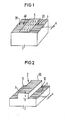
- the procedure is such that in the surface of a wafer 3 with the epitaxial layer system required for later use, which are not shown in the figures, a surface grid 4 with a chemical anisotropic etchant is used V-shaped grooves is etched by exposing the (111) faces of the crystal material of the substrate below the surface 40.
- This surface grid 4 extends over the entire surface 40 and has the lattice constant a.
- Photoresist is used as the mask, which is exposed by means of an interference pattern.
- photoresist is again applied to the surface grid 4, so that it lies tightly everywhere on the relief of this grid.
- a photoresist strip 5 is generated by mask exposure, the longitudinal direction of which extends transversely, for example perpendicularly, to the grooves of the surface grid 4 and under which the raised area 30 is formed.
- the remaining areas 20 of the surface grid 4, which adjoin the long sides of the photoresist strip 5, are completely exposed so that the etchant can act on these areas 20 unhindered during the production of the step structure 2.
- the surface 40 with the photoresist strip 5 thereon is etched with the same etchant as in the production of the surface grid 4.
- this grid is transferred in the areas 20 laterally next to the photoresist strip 5 unchanged in depth.
- the lower-lying surface regions 10 with the desired surface grids 1 are formed, which border on the intermediate strip-like raised region 30 on which the rest of the surface grid 4 according to FIG. 1 has remained.
- the grid that has stopped and the grid 1 on the lower regions 1 1 D have the same phase position and the same grid constant a.
- a substrate 3 made of a III-V semiconductor was etched with an etchant which consisted of a mixture of sulfuric acid, hydrogen peroxide and water, for example about 3 parts from a 25% strength sulfuric acid, 8 parts of 30% hydrogen peroxide and 35 parts of water. The percentages are percentages by volume.
- the surface of the substrate was etched with this etchant for approximately 1 minute to produce the surface grid 4, and for approximately 1-5 minutes to produce the step structure 2, the sinking depth b being 0.2-1.4 ⁇ m.
- the lattice constant a was about 0.3 ⁇ m in the submicron range. It is expedient to carry out the etching processes at low temperatures, for example at or near 0 ° C.
Applications Claiming Priority (2)
| Application Number | Priority Date | Filing Date | Title |
|---|---|---|---|
| DE3514301 | 1985-04-19 | ||
| DE3514301 | 1985-04-19 |
Publications (1)
| Publication Number | Publication Date |
|---|---|
| EP0200874A1 true EP0200874A1 (fr) | 1986-11-12 |
Family
ID=6268683
Family Applications (1)
| Application Number | Title | Priority Date | Filing Date |
|---|---|---|---|
| EP86102897A Ceased EP0200874A1 (fr) | 1985-04-19 | 1986-03-05 | Procédé pour la fabrication d'un réseau ayant une constante de réseau déterminée sur une surface enfoncée d'une structure mésa |
Country Status (2)
| Country | Link |
|---|---|
| EP (1) | EP0200874A1 (fr) |
| JP (1) | JPS61242026A (fr) |
Cited By (1)
| Publication number | Priority date | Publication date | Assignee | Title |
|---|---|---|---|---|
| EP0282878A2 (fr) * | 1987-03-16 | 1988-09-21 | Siemens Aktiengesellschaft | Dispositif de spectromètre optique intégré et son procédé de fabrication |
Families Citing this family (3)
| Publication number | Priority date | Publication date | Assignee | Title |
|---|---|---|---|---|
| DE102014108301A1 (de) * | 2014-06-12 | 2015-12-17 | Osram Opto Semiconductors Gmbh | Halbleiterchip und Verfahren zur Herstellung eines Halbleiterchips |
| WO2016031712A1 (fr) * | 2014-08-26 | 2016-03-03 | 日本碍子株式会社 | Élément de réseau |
| CN108802881B (zh) * | 2018-05-21 | 2022-03-08 | 苏州大学 | 一种高衍射效率光栅结构和制备方法 |
Citations (5)
| Publication number | Priority date | Publication date | Assignee | Title |
|---|---|---|---|---|
| US4217148A (en) * | 1979-06-18 | 1980-08-12 | Rca Corporation | Compensated amorphous silicon solar cell |
| EP0051980A1 (fr) * | 1980-11-10 | 1982-05-19 | Atlantic Richfield Company | Dispositif photovoltaique et électrode pour une cellule photoélectrochimique |
| US4396793A (en) * | 1982-04-12 | 1983-08-02 | Chevron Research Company | Compensated amorphous silicon solar cell |
| US4409424A (en) * | 1982-06-21 | 1983-10-11 | Genevieve Devaud | Compensated amorphous silicon solar cell |
| GB2135510A (en) * | 1982-12-23 | 1984-08-30 | Semiconductor Energy Lab | Photoelectric conversion devices |
-
1986
- 1986-03-05 EP EP86102897A patent/EP0200874A1/fr not_active Ceased
- 1986-04-16 JP JP8784286A patent/JPS61242026A/ja active Pending
Patent Citations (5)
| Publication number | Priority date | Publication date | Assignee | Title |
|---|---|---|---|---|
| US4217148A (en) * | 1979-06-18 | 1980-08-12 | Rca Corporation | Compensated amorphous silicon solar cell |
| EP0051980A1 (fr) * | 1980-11-10 | 1982-05-19 | Atlantic Richfield Company | Dispositif photovoltaique et électrode pour une cellule photoélectrochimique |
| US4396793A (en) * | 1982-04-12 | 1983-08-02 | Chevron Research Company | Compensated amorphous silicon solar cell |
| US4409424A (en) * | 1982-06-21 | 1983-10-11 | Genevieve Devaud | Compensated amorphous silicon solar cell |
| GB2135510A (en) * | 1982-12-23 | 1984-08-30 | Semiconductor Energy Lab | Photoelectric conversion devices |
Non-Patent Citations (1)
| Title |
|---|
| JOURNAL OF APPLIED PHYSICS, Band 54, Nr. 11, November 1983, Seiten 6705-6707, American Institute of Physics, New York, US; P. SICHANUGRIST et al.: "Amorphous silicon solar cells with graded boron-doped active layers" * |
Cited By (2)
| Publication number | Priority date | Publication date | Assignee | Title |
|---|---|---|---|---|
| EP0282878A2 (fr) * | 1987-03-16 | 1988-09-21 | Siemens Aktiengesellschaft | Dispositif de spectromètre optique intégré et son procédé de fabrication |
| EP0282878A3 (en) * | 1987-03-16 | 1989-09-20 | Siemens Aktiengesellschaft | Arrangement of optical-integrated spectrometer and method for the making the same |
Also Published As
| Publication number | Publication date |
|---|---|
| JPS61242026A (ja) | 1986-10-28 |
Similar Documents
| Publication | Publication Date | Title |
|---|---|---|
| DE2628407C2 (de) | Verfahren zum Herstellen von dielektrischen Isolationszonen | |
| DE2652294C2 (de) | Verfahren zum Herstellen eingelegter Oxidbereiche in Halbleitersubstraten | |
| DE2550056A1 (de) | Iii-v-photokathode und verfahren zu ihrer herstellung | |
| DE2615754C2 (fr) | ||
| DE19504117A1 (de) | Quantenverdrahtung und Verfahren zu deren Herstellung | |
| DE3034078A1 (de) | Verfahren zur herstellung einer halbleiteranordnung | |
| DE2265257C2 (de) | Verfahren zur Herstellung einer integrierten Halbleiterschaltung | |
| DE2608562A1 (de) | Halbleiteranordnung zum erzeugen inkohaerenter strahlung und verfahren zu deren herstellung | |
| DE3540422C2 (de) | Verfahren zum Herstellen integrierter Strukturen mit nicht-flüchtigen Speicherzellen, die selbst-ausgerichtete Siliciumschichten und dazugehörige Transistoren aufweisen | |
| DE3610333A1 (de) | Verfahren zur herstellung eines oberflaechengitters mit einer bestimmten gitterkonstanten auf einem tieferliegenden oberflaechenbereich einer mesastruktur | |
| DE4412027C2 (de) | Verfahren zum Herstellen einer sichtbares Licht erzeugenden Halbleiter-Laserdiode | |
| DE3537047A1 (de) | Schnabelreduzierendes planox-verfahren fuer die herstellung integrierter elektronischer komponenten | |
| DE2540352A1 (de) | Verfahren zur selektiven oxydation | |
| DE2920454A1 (de) | Halbleiterlaser und verfahren zu dessen herstellung | |
| DE4010889A1 (de) | Verfahren zum herstellen einer vergrabenen laserdiode mit heterostruktur | |
| DE1814747C2 (de) | Verfahren zum Herstellen von Feldefekttransistoren | |
| EP0200874A1 (fr) | Procédé pour la fabrication d'un réseau ayant une constante de réseau déterminée sur une surface enfoncée d'une structure mésa | |
| EP0218039B1 (fr) | Procédé pour transmettre des structures à photorésist les plus fines | |
| EP0257328A1 (fr) | Procédé pour fabriquer des jonctions du type PN | |
| EP0240776A1 (fr) | Procédé de fabrication d'un réseau de surface avec une constante de réseau déterminée dans un plan inférieur d'une structure mésa | |
| DE4445566A1 (de) | Verfahren zur Herstellung einer optischen integrierten Schaltung | |
| DE2755168A1 (de) | Verfahren zur herstellung von halbleiterbauelementen | |
| EP0198199A2 (fr) | Procédé d'attaque chimique pour la formation d'un réseau de surface à constante de réseau déterminée sur la surface d'un substrat en un matériau cristallin | |
| DE10219886A1 (de) | Selbstjustierendes Verfahren zur Herstellung eines Steghohlleitung-Halbleiterlasers | |
| EP0003733B1 (fr) | Procédé pour la génération de fenêtres échelonnées dans des couches de matière isolante ou de matière d'électrode pour la production de circuits intégrés à semiconducteur et transistor MIS à effet de champ avec courte longueur de canal fabriqué par ce procédé |
Legal Events
| Date | Code | Title | Description |
|---|---|---|---|
| PUAI | Public reference made under article 153(3) epc to a published international application that has entered the european phase |
Free format text: ORIGINAL CODE: 0009012 |
|
| AK | Designated contracting states |
Kind code of ref document: A1 Designated state(s): DE FR GB |
|
| PUAB | Information related to the publication of an a document modified or deleted |
Free format text: ORIGINAL CODE: 0009199EPPU |
|
| PUAF | Information related to the publication of a search report (a3 document) modified or deleted |
Free format text: ORIGINAL CODE: 0009199SEPU |
|
| R17D | Deferred search report published (corrected) |
Effective date: 19861217 |
|
| RA1 | Application published (corrected) |
Date of ref document: 19861217 Kind code of ref document: A1 |
|
| 17P | Request for examination filed |
Effective date: 19870522 |
|
| 17Q | First examination report despatched |
Effective date: 19890619 |
|
| STAA | Information on the status of an ep patent application or granted ep patent |
Free format text: STATUS: THE APPLICATION HAS BEEN REFUSED |
|
| 18R | Application refused |
Effective date: 19900707 |
|
| RIN1 | Information on inventor provided before grant (corrected) |
Inventor name: MAERZ, REINHARD, DR. Inventor name: HEISE, GERHARD, DIPL.-PHYS. |