EP0200874A1 - Process for making a surface grating having a specified operating constant on a recessed surface of a mesa structure - Google Patents
Process for making a surface grating having a specified operating constant on a recessed surface of a mesa structure Download PDFInfo
- Publication number
- EP0200874A1 EP0200874A1 EP86102897A EP86102897A EP0200874A1 EP 0200874 A1 EP0200874 A1 EP 0200874A1 EP 86102897 A EP86102897 A EP 86102897A EP 86102897 A EP86102897 A EP 86102897A EP 0200874 A1 EP0200874 A1 EP 0200874A1
- Authority
- EP
- European Patent Office
- Prior art keywords
- lattice
- grating
- finely structured
- mesa structure
- substrate
- Prior art date
- Legal status (The legal status is an assumption and is not a legal conclusion. Google has not performed a legal analysis and makes no representation as to the accuracy of the status listed.)
- Ceased
Links
Images
Classifications
-
- H—ELECTRICITY
- H01—ELECTRIC ELEMENTS
- H01L—SEMICONDUCTOR DEVICES NOT COVERED BY CLASS H10
- H01L33/00—Semiconductor devices with at least one potential-jump barrier or surface barrier specially adapted for light emission; Processes or apparatus specially adapted for the manufacture or treatment thereof or of parts thereof; Details thereof
- H01L33/02—Semiconductor devices with at least one potential-jump barrier or surface barrier specially adapted for light emission; Processes or apparatus specially adapted for the manufacture or treatment thereof or of parts thereof; Details thereof characterised by the semiconductor bodies
- H01L33/16—Semiconductor devices with at least one potential-jump barrier or surface barrier specially adapted for light emission; Processes or apparatus specially adapted for the manufacture or treatment thereof or of parts thereof; Details thereof characterised by the semiconductor bodies with a particular crystal structure or orientation, e.g. polycrystalline, amorphous or porous
-
- H—ELECTRICITY
- H01—ELECTRIC ELEMENTS
- H01L—SEMICONDUCTOR DEVICES NOT COVERED BY CLASS H10
- H01L21/00—Processes or apparatus adapted for the manufacture or treatment of semiconductor or solid state devices or of parts thereof
- H01L21/02—Manufacture or treatment of semiconductor devices or of parts thereof
- H01L21/04—Manufacture or treatment of semiconductor devices or of parts thereof the devices having at least one potential-jump barrier or surface barrier, e.g. PN junction, depletion layer or carrier concentration layer
- H01L21/18—Manufacture or treatment of semiconductor devices or of parts thereof the devices having at least one potential-jump barrier or surface barrier, e.g. PN junction, depletion layer or carrier concentration layer the devices having semiconductor bodies comprising elements of Group IV of the Periodic System or AIIIBV compounds with or without impurities, e.g. doping materials
- H01L21/30—Treatment of semiconductor bodies using processes or apparatus not provided for in groups H01L21/20 - H01L21/26
- H01L21/302—Treatment of semiconductor bodies using processes or apparatus not provided for in groups H01L21/20 - H01L21/26 to change their surface-physical characteristics or shape, e.g. etching, polishing, cutting
- H01L21/306—Chemical or electrical treatment, e.g. electrolytic etching
- H01L21/30604—Chemical etching
- H01L21/30612—Etching of AIIIBV compounds
- H01L21/30617—Anisotropic liquid etching
-
- H—ELECTRICITY
- H01—ELECTRIC ELEMENTS
- H01L—SEMICONDUCTOR DEVICES NOT COVERED BY CLASS H10
- H01L33/00—Semiconductor devices with at least one potential-jump barrier or surface barrier specially adapted for light emission; Processes or apparatus specially adapted for the manufacture or treatment thereof or of parts thereof; Details thereof
- H01L33/005—Processes
-
- H—ELECTRICITY
- H01—ELECTRIC ELEMENTS
- H01L—SEMICONDUCTOR DEVICES NOT COVERED BY CLASS H10
- H01L33/00—Semiconductor devices with at least one potential-jump barrier or surface barrier specially adapted for light emission; Processes or apparatus specially adapted for the manufacture or treatment thereof or of parts thereof; Details thereof
- H01L33/02—Semiconductor devices with at least one potential-jump barrier or surface barrier specially adapted for light emission; Processes or apparatus specially adapted for the manufacture or treatment thereof or of parts thereof; Details thereof characterised by the semiconductor bodies
- H01L33/20—Semiconductor devices with at least one potential-jump barrier or surface barrier specially adapted for light emission; Processes or apparatus specially adapted for the manufacture or treatment thereof or of parts thereof; Details thereof characterised by the semiconductor bodies with a particular shape, e.g. curved or truncated substrate
Definitions
- the present invention relates to a method for producing a surface lattice with a specific lattice constant on a lower surface area of a stepped structure according to the preamble of patent claim 1.
- the object of the present invention is to provide a particularly simple and very inexpensive method of the type mentioned at the outset.
- the step structure is etched into a finely structured surface of the substrate having a surface lattice with the specific lattice constant by means of an anisotropic etching agent which is the slowest etching in at least one direction oblique to the finely structured surface , wherein in a mask-free area defining the underlying surface area of the stepped structure, the relief of the surface lattice of the masked, finely structured surface exposed to the anisotropic etchant is transferred more or less true to shape but while maintaining the certain lattice constants, where, after the etching process has ended, the desired surface lattice is transferred forms.
- the method according to the invention is self-adjusting.
- the surface of the substrate only has to satisfy the condition that its lattice constant matches the lattice constant of the desired surface lattice on the lower surface area. Otherwise, the profile of the grooves of the surface lattice of the finely structured surface of the substrate can largely have any shape.
- This grating can be designed, for example, to be slightly wavy or else have a rectangular groove profile.
- the surface lattice of the finely structured surface of the substrate is produced by wet chemical etching with at least essentially the same anisotropic etchant as is used in the etching of the step structure.
- the surface lattice of the finely structured surface of the substrate already has the same groove profile as the desired surface lattice.
- the surface lattice of the finely structured surface of the substrate is transmitted essentially unchanged in depth, as a result of which very good reproducibility of the lattice can be obtained on the lower surface area.
- the areas of the structured surface covered by the mask remain as raised areas which are separated from the lower-lying areas by a step transition.
- step structure is to be understood in general so that the structure has steps.
- the surface lattice of the finely structured surface remains, with which the surface lattice lowered in depth remains the same Has phase position.
- This remaining surface grid on the raised areas of the stepped structure can be used for gain coupling in the case of the MCRW laser, where this raised area is strip-shaped, since a modulation of the injection current takes place via the spatially changing contact resistance.
- the relatively simple step structure indicated by the figures relates to the production of an MCRW laser, which essentially only requires a strip-like raised area.
- the method can also be used for more complicated step structures.
- the procedure is such that in the surface of a wafer 3 with the epitaxial layer system required for later use, which are not shown in the figures, a surface grid 4 with a chemical anisotropic etchant is used V-shaped grooves is etched by exposing the (111) faces of the crystal material of the substrate below the surface 40.
- This surface grid 4 extends over the entire surface 40 and has the lattice constant a.
- Photoresist is used as the mask, which is exposed by means of an interference pattern.
- photoresist is again applied to the surface grid 4, so that it lies tightly everywhere on the relief of this grid.
- a photoresist strip 5 is generated by mask exposure, the longitudinal direction of which extends transversely, for example perpendicularly, to the grooves of the surface grid 4 and under which the raised area 30 is formed.
- the remaining areas 20 of the surface grid 4, which adjoin the long sides of the photoresist strip 5, are completely exposed so that the etchant can act on these areas 20 unhindered during the production of the step structure 2.
- the surface 40 with the photoresist strip 5 thereon is etched with the same etchant as in the production of the surface grid 4.
- this grid is transferred in the areas 20 laterally next to the photoresist strip 5 unchanged in depth.
- the lower-lying surface regions 10 with the desired surface grids 1 are formed, which border on the intermediate strip-like raised region 30 on which the rest of the surface grid 4 according to FIG. 1 has remained.
- the grid that has stopped and the grid 1 on the lower regions 1 1 D have the same phase position and the same grid constant a.
- a substrate 3 made of a III-V semiconductor was etched with an etchant which consisted of a mixture of sulfuric acid, hydrogen peroxide and water, for example about 3 parts from a 25% strength sulfuric acid, 8 parts of 30% hydrogen peroxide and 35 parts of water. The percentages are percentages by volume.
- the surface of the substrate was etched with this etchant for approximately 1 minute to produce the surface grid 4, and for approximately 1-5 minutes to produce the step structure 2, the sinking depth b being 0.2-1.4 ⁇ m.
- the lattice constant a was about 0.3 ⁇ m in the submicron range. It is expedient to carry out the etching processes at low temperatures, for example at or near 0 ° C.
Abstract
Description
Die vorliegende Erfindung betrifft ein Verfahren zur Herstellung eines Oberflächengitters mit einer bestimmten Gitterkonstanten auf einem tieferliegenden Oberflächenbereich einer stufigen Struktur nach dem Oberbegriff des Patentanspruchs 1.The present invention relates to a method for producing a surface lattice with a specific lattice constant on a lower surface area of a stepped structure according to the preamble of patent claim 1.
Für die Realisierung eines DFB-MCRW-Lasers in Einschrittepitaxie ist es notwendig, Gitter in einem tieferliegenden Bereich unmittelbar neben einem erhabenen Bereich einer Mesastruktur herzustellen. Ein DFB-MCRW-Laser und seine Herstellung in Einschrittepitaxie ist in der älteren Patentanmeidung P 34 37 209.1 mit dem Titel "Verbesserung zu einem Monornoden-Diodenlaser" vorgeschlagen.For the implementation of a DFB-MCRW laser in one-step epitaxy, it is necessary to produce grids in a lower area immediately next to a raised area of a mesa structure. A DFB-MCRW laser and its manufacture in one-step epitaxy is proposed in the older patent application P 34 37 209.1 with the title "Improvement to a monode diode laser".
Denkbar wäre es, das Oberflächengitter auf dem tieferliegenden Bereich durch ein Verfahren mit Mehrlagenmaskierung herzustellen. Dabei muß aber das Problem umgangen werden, daß Fotolack auf Substrate bzw. Wafer mit Mesastrukturen nicht aufgeschleudert werden kann.It would be conceivable to produce the surface lattice on the lower-lying area using a method with multi-layer masking. However, the problem must be avoided that photoresist cannot be spun onto substrates or wafers with mesa structures.
Aufgabe der vorliegenden Erfindung ist es, ein besonders einfaches und sehr billiges Verfahren der eingangs genannten Art anzugeben.The object of the present invention is to provide a particularly simple and very inexpensive method of the type mentioned at the outset.
Diese Aufgabe wird gemäß dem kennzeichnenden Teil des Patentanspruchs 1 dadurch gelöst, daß die stufige Struktur in eine fein strukturierte, ein Oberflächengitter mit der bestimmten Gitterkonstanten aufweisende Oberfläche des Substrats mittels eines anisotropen, in zumindest einer zur feinstrukturierten Oberfläche schrägen Richtung am langsamsten ätzenden Ätzmittels geätzt wird, wobei in einem den tieferliegenden Oberflächenbereich der stufigen Struktur definierenden maskenfreien Bereich das Relief des dem anisotropen Ätzmittel ausgesetzten Oberflächengitters der maskierten feinstrukturierten Oberfläche mehr oder weniger formgetreu aber unter Beibehaltung der bestimmten Gitterkonstanten in die Tiefe übertragen wird, wo es nach Beendigung des Ätzvorganges das gewünschte Oberflächengitter bildet.This object is achieved according to the characterizing part of claim 1 in that the step structure is etched into a finely structured surface of the substrate having a surface lattice with the specific lattice constant by means of an anisotropic etching agent which is the slowest etching in at least one direction oblique to the finely structured surface , wherein in a mask-free area defining the underlying surface area of the stepped structure, the relief of the surface lattice of the masked, finely structured surface exposed to the anisotropic etchant is transferred more or less true to shape but while maintaining the certain lattice constants, where, after the etching process has ended, the desired surface lattice is transferred forms.
Das erfindungsgemäße Verfahren ist selbstjustierend. Das Oberflächengitter der feinstrukturierten. Oberfläche des Substrats muß nur der Bedingung genügen, daß seine Gitterkonstante mit der Gitterkonstanten des gewünschten Oberflächengitters auf dem tieferliegenden Oberflächenbereich übereinstimmt. Ansonsten kann das Profil der Rillen des Oberflächengitters der feinstrukturierten Oberfläche des Substrats weitgehend eine beliebige Form aufweisen. Dieses Gitter kann beispielsweise schwach wellig ausgebildet sein oder aber auch ein rechteckförmiges Rillenprofil aufweisen.The method according to the invention is self-adjusting. The surface grid of the finely structured. The surface of the substrate only has to satisfy the condition that its lattice constant matches the lattice constant of the desired surface lattice on the lower surface area. Otherwise, the profile of the grooves of the surface lattice of the finely structured surface of the substrate can largely have any shape. This grating can be designed, for example, to be slightly wavy or else have a rectangular groove profile.
Vorteilhaft ist es aber, wenn gemäß dem Patentanspruch 2 das Oberflächengitter der feinstrukturierten Oberfläche des Substrats durch naßchemisches Ätzen mit zumindest im wesentlichen dem gleichen anisotropen Ätzmittel hergestellt wird, wie es beim Ätzen der stufigen Struktur verwendet wird. In diesem Fall hat das Oberflächengitter der feinstrukturierten Oberfläche des Substrats bereits von vomeherein das gleiche Rillenprofil, wie das gewünschte Oberflächengitter. Das Oberflächengitter der feinstrukturierten Oberfläche des Substrats wird in diesem Fall im wesentlichen unverändert in die Tiefe übertragen, wodurch eine sehr gute Reproduzierbarkeit des Gitters auf dem tieferliegenden Oberflächenbereich erhalten werden kann.However, it is advantageous if, according to
Bei dem erfindungsgemäßen Verfahren bleiben die von der Maske abgedeckten Bereiche der strukturierten Oberfläche als erhabene Bereiche stehen, die durch einen Stufenübergang von den tieferliegenden Bereichen getrennt sind. Der Begriff "stufige Struktur" ist allgemein so aufzufassen, daß die Struktur Stufen aufweist. Unter der Maske, die auf dem Relief der feinstrukturierten Oberfläche dicht aufliegt, so daß in die von ihr abgedeckten feinstrukturierten Oberflächenbereiche von der Seite her kein Ätzmittel eindringen kann, bleibt das Oberflächengitter der feinstrukturierten Oberfläche stehen, mit der das in die Tiefe abgesenkte Oberflächengitter die gleiche Phasenlage aufweist. Dieses stehengebliebene Oberflächengitter auf den erhabenen Bereichen der gestuften Struktur kann im Fall des MCRW-Lasers, wo dieser erhabene Bereich streifenförmig ausgebildet ist, zur Gainkopplung verwendet werden, da über den sich räumlich ändemden Übergangswiderstand eine Modulation des Injektionsstromes stattfindet.In the method according to the invention, the areas of the structured surface covered by the mask remain as raised areas which are separated from the lower-lying areas by a step transition. The term "step structure" is to be understood in general so that the structure has steps. Under the mask, which rests tightly on the relief of the finely structured surface, so that no etchant can penetrate from the side into the finely structured surface areas covered by it, the surface lattice of the finely structured surface remains, with which the surface lattice lowered in depth remains the same Has phase position. This remaining surface grid on the raised areas of the stepped structure can be used for gain coupling in the case of the MCRW laser, where this raised area is strip-shaped, since a modulation of the injection current takes place via the spatially changing contact resistance.
Die Erfindung wird beispielhaft anhand der Figuren in der folgenden Beschreibung näher erläutert. Von den Figuren zeigen:
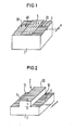
- Figur 1 in perspektivischer Darstellung ein Substrat mit einer feinstrukturierten Oberfläche in Form eines Oberflächengitters mit im Profil dreieckförmigen Rillen, das zur Herstellung einer Mesastruktur mit einer streifenförmigen Ätzmaske abgedeckt ist, und
Figur 2 das Gebilde nach Figur 1 in der gleichen Darstellung nach dem Ätzen der stufigen Struktur.
- FIG. 1 shows a perspective representation of a substrate with a finely structured surface in the form of a surface grid with triangular-shaped grooves, which is covered with a strip-shaped etching mask in order to produce a mesa structure, and
- Figure 2 shows the structure of Figure 1 in the same representation after the etching of the step structure.
Die durch die Figuren angedeutete relativ einfache stufige Struktur bezieht sich auf die Herstellung eines MCRW-Lasers, der im wesentlichen nur einen streifenförmigen erhabenen Bereich benötigt. Selbstverständlich kann das Verfahren auch für kompliziertere stufige Strukturen verwendet werden.The relatively simple step structure indicated by the figures relates to the production of an MCRW laser, which essentially only requires a strip-like raised area. Of course, the method can also be used for more complicated step structures.
Zur Herstellung der feinstrukturierten Oberfläche 40 nach Figur 1 wird beispielsweise so vorgegangen, daß in die Oberfläche eines Wafers 3 mit den für die spätere Verwendung erforderlichen epitaktischen Schichtsystem, die in den Figuren nicht dargestellt sind, naßchemisch mit einem anisotropen Ätzmittel ein Oberflächengitter 4 mit im Profil V-förmigen Rillen geätzt wird, und zwar durch Freilegen der (111 )-Flächen des Kristallmaterials des Substrats unter der Oberfläche 40. Dieses Oberflächengitter 4 erstreckt sich über die ganze Oberfläche 40 und weist die Gitterkonstante a auf. Als Maske wird Fotolack verwendet, der mittels eines Interferenzmusters belichtet wird.To produce the finely structured
Zur Herstellung der stufigen Struktur 2 nach Figur 2 mit dem streifenförmigen erhabenen Bereich 30 wird auf das Oberflächengitter 4 erneut Fotolack aufgetragen, so, daß er auf dem Relief dieses Gitters überall dicht aufliegt. Durch Maskenbelichtung wird ein Fotoresist-Streifen 5 erzeugt, dessen Längsrichtung quer, beispielsweise senkrecht, zu den Rillen des Oberflächengitters 4 verläuft, und unter dem der erhabene Bereich 30 entsteht. Die übrigen Bereiche 20 des Oberflächengitters 4, die an die Längsseiten des Fotoresist-Streifens 5 grenzen, werden ganz freigelegt, damit bei der Herstellung der stufigen Struktur 2 das Ätzmittel ungehindert auf diese Bereiche 20 einwirken kann. Dabei wird die Oberfläche 40 mit dem darauf befindlichen Fotoresist-Streifen 5 mit dem gleichen Ätzmittel wie bei der Herstellung des Oberflächengitters 4 geätzt. Dadurch wird dieses Gitter in den Bereichen 20 seitlich neben dem Fotoresist-Streifen 5 unverändert in die Tiefe übertragen. Es entstehen die tieferliegenden Oberflächenbereiche 10 mit den gewünschten Oberflächengittern 1, die an den dazwischenliegenden streifenförmigen erhabenen Bereich 30 grenzen, auf dem der Rest des Oberflächengitters 4 nach Figur 1 stehengeblieben ist. Das stehengebliebene Gitter und die Gitter 1 auf den tieferliegenden Bereichen 11D haben die gleiche Phasenlage und die gleiche GItterkonstante a.To produce the
Bei der praktischen Realisierung einer solchen stufigen Struktur 2 wurde beispielsweise ein Substrat 3 aus einem III-V-Halbleiter mit einem Ätzmittel geätzt, das aus einer Mischung aus Schwefelsäure, Wasserstoffperoxid und Wasser bestand, beispielsweise aus ungefähr 3 Teilen aus einer 25 %igen Schwefelsäure, 8 Teilen 30 %igem Wasserstoffperoxid und aus 35 Teilen Wasser. Die Prozentangaben verstehen sich als Volumenprozente.In the practical implementation of such a
Zur Herstellung des Oberflächengitters 4 wurde die Oberfläche des Substrats etwa 1 Minute lang mit diesem Ätzmittel geätzt, und zur Herstellung der stufigen Struktur 2 wurde etwa 1 -5 Minuten lang geätzt, wobei die Versenktiefe b von 0,2 -1,4 um beträgt. Die Gitterkonstante a lag im Submikronbereich etwa bei 0,3 um. Günstig ist es , die Ätzvorgänge bei niedrigen Temperaturen, beispielsweise bei oder in der Nähe von 0°C vorzunehmen.The surface of the substrate was etched with this etchant for approximately 1 minute to produce the
Claims (2)
Applications Claiming Priority (2)
| Application Number | Priority Date | Filing Date | Title |
|---|---|---|---|
| DE3514301 | 1985-04-19 | ||
| DE3514301 | 1985-04-19 |
Publications (1)
| Publication Number | Publication Date |
|---|---|
| EP0200874A1 true EP0200874A1 (en) | 1986-11-12 |
Family
ID=6268683
Family Applications (1)
| Application Number | Title | Priority Date | Filing Date |
|---|---|---|---|
| EP86102897A Ceased EP0200874A1 (en) | 1985-04-19 | 1986-03-05 | Process for making a surface grating having a specified operating constant on a recessed surface of a mesa structure |
Country Status (2)
| Country | Link |
|---|---|
| EP (1) | EP0200874A1 (en) |
| JP (1) | JPS61242026A (en) |
Cited By (1)
| Publication number | Priority date | Publication date | Assignee | Title |
|---|---|---|---|---|
| EP0282878A2 (en) * | 1987-03-16 | 1988-09-21 | Siemens Aktiengesellschaft | Arrangement of optical-integrated spectrometer and method for the making the same |
Families Citing this family (3)
| Publication number | Priority date | Publication date | Assignee | Title |
|---|---|---|---|---|
| DE102014108301A1 (en) * | 2014-06-12 | 2015-12-17 | Osram Opto Semiconductors Gmbh | Semiconductor chip and method for producing a semiconductor chip |
| JP6613238B2 (en) * | 2014-08-26 | 2019-11-27 | 日本碍子株式会社 | Grating element |
| CN108802881B (en) * | 2018-05-21 | 2022-03-08 | 苏州大学 | High diffraction efficiency grating structure and preparation method thereof |
Citations (5)
| Publication number | Priority date | Publication date | Assignee | Title |
|---|---|---|---|---|
| US4217148A (en) * | 1979-06-18 | 1980-08-12 | Rca Corporation | Compensated amorphous silicon solar cell |
| EP0051980A1 (en) * | 1980-11-10 | 1982-05-19 | Atlantic Richfield Company | Photovoltaic device and photoelectrochemical cell electrode |
| US4396793A (en) * | 1982-04-12 | 1983-08-02 | Chevron Research Company | Compensated amorphous silicon solar cell |
| US4409424A (en) * | 1982-06-21 | 1983-10-11 | Genevieve Devaud | Compensated amorphous silicon solar cell |
| GB2135510A (en) * | 1982-12-23 | 1984-08-30 | Semiconductor Energy Lab | Photoelectric conversion devices |
-
1986
- 1986-03-05 EP EP86102897A patent/EP0200874A1/en not_active Ceased
- 1986-04-16 JP JP8784286A patent/JPS61242026A/en active Pending
Patent Citations (5)
| Publication number | Priority date | Publication date | Assignee | Title |
|---|---|---|---|---|
| US4217148A (en) * | 1979-06-18 | 1980-08-12 | Rca Corporation | Compensated amorphous silicon solar cell |
| EP0051980A1 (en) * | 1980-11-10 | 1982-05-19 | Atlantic Richfield Company | Photovoltaic device and photoelectrochemical cell electrode |
| US4396793A (en) * | 1982-04-12 | 1983-08-02 | Chevron Research Company | Compensated amorphous silicon solar cell |
| US4409424A (en) * | 1982-06-21 | 1983-10-11 | Genevieve Devaud | Compensated amorphous silicon solar cell |
| GB2135510A (en) * | 1982-12-23 | 1984-08-30 | Semiconductor Energy Lab | Photoelectric conversion devices |
Non-Patent Citations (1)
| Title |
|---|
| JOURNAL OF APPLIED PHYSICS, Band 54, Nr. 11, November 1983, Seiten 6705-6707, American Institute of Physics, New York, US; P. SICHANUGRIST et al.: "Amorphous silicon solar cells with graded boron-doped active layers" * |
Cited By (2)
| Publication number | Priority date | Publication date | Assignee | Title |
|---|---|---|---|---|
| EP0282878A2 (en) * | 1987-03-16 | 1988-09-21 | Siemens Aktiengesellschaft | Arrangement of optical-integrated spectrometer and method for the making the same |
| EP0282878A3 (en) * | 1987-03-16 | 1989-09-20 | Siemens Aktiengesellschaft | Arrangement of optical-integrated spectrometer and method for the making the same |
Also Published As
| Publication number | Publication date |
|---|---|
| JPS61242026A (en) | 1986-10-28 |
Similar Documents
| Publication | Publication Date | Title |
|---|---|---|
| DE2628407C2 (en) | Process for producing dielectric isolation zones | |
| DE2652294C2 (en) | Process for producing embedded oxide regions in semiconductor substrates | |
| DE2550056A1 (en) | III-V PHOTOCATHOD AND METHOD OF MANUFACTURING IT | |
| DE2615754C2 (en) | ||
| DE19504117A1 (en) | Prodn. of quantum wire for semiconductor lasers | |
| DE3034078A1 (en) | METHOD FOR PRODUCING A SEMICONDUCTOR ARRANGEMENT | |
| DE2265257C2 (en) | Method for manufacturing an integrated semiconductor circuit | |
| DE2608562A1 (en) | Semiconductor arrangement for generating incoherent radiation | |
| DE3540422C2 (en) | Method for producing integrated structures with non-volatile memory cells which have self-aligned silicon layers and associated transistors | |
| DE3610333A1 (en) | Method for producing a surface grating (lattice, grid) having a specific grating constant on a lower-lying surface region of a mesastructure | |
| DE4412027C2 (en) | Method for producing a visible light-producing semiconductor laser diode | |
| DE3537047A1 (en) | BOTTLE-REDUCING PLANOX METHOD FOR THE PRODUCTION OF INTEGRATED ELECTRONIC COMPONENTS | |
| DE2540352A1 (en) | METHOD OF SELECTIVE OXYDATION | |
| DE2920454A1 (en) | SEMICONDUCTOR LASERS AND THE PROCESS FOR THE PRODUCTION THEREOF | |
| DE4010889A1 (en) | Manufacture of laser diode with heterostructure - using masking and etching processes to form layers | |
| DE1814747C2 (en) | Process for the production of field defect transistors | |
| EP0200874A1 (en) | Process for making a surface grating having a specified operating constant on a recessed surface of a mesa structure | |
| EP0218039B1 (en) | Method for transferring the finest photoresist structures | |
| EP0257328A1 (en) | Method of producing pn junctions | |
| EP0240776A1 (en) | Method for manufacturing a surface grating with a predetermined lattice constant in a lower surface region of a mesa structure | |
| DE4445566A1 (en) | Optical integrated circuit prodn. process | |
| DE2755168A1 (en) | METHOD FOR MANUFACTURING SEMICONDUCTOR COMPONENTS | |
| EP0198199A2 (en) | Wet etching process for making a surface grating having a specified operating constant on the surface of a substrate of a semiconductor material | |
| EP0003733B1 (en) | Process for the generation of windows having stepped edges within material layers of insulating material or of material for electrodes for the production of an integrated semiconductor circuit and mis field-effect transistor with short channel length produced by this process | |
| EP0938746B1 (en) | Process for wet chemical etching or surface cleaning of mixed crystal compounds containing arsenic |
Legal Events
| Date | Code | Title | Description |
|---|---|---|---|
| PUAI | Public reference made under article 153(3) epc to a published international application that has entered the european phase |
Free format text: ORIGINAL CODE: 0009012 |
|
| AK | Designated contracting states |
Kind code of ref document: A1 Designated state(s): DE FR GB |
|
| PUAB | Information related to the publication of an a document modified or deleted |
Free format text: ORIGINAL CODE: 0009199EPPU |
|
| PUAF | Information related to the publication of a search report (a3 document) modified or deleted |
Free format text: ORIGINAL CODE: 0009199SEPU |
|
| R17D | Deferred search report published (corrected) |
Effective date: 19861217 |
|
| RA1 | Application published (corrected) |
Date of ref document: 19861217 Kind code of ref document: A1 |
|
| 17P | Request for examination filed |
Effective date: 19870522 |
|
| 17Q | First examination report despatched |
Effective date: 19890619 |
|
| STAA | Information on the status of an ep patent application or granted ep patent |
Free format text: STATUS: THE APPLICATION HAS BEEN REFUSED |
|
| 18R | Application refused |
Effective date: 19900707 |
|
| RIN1 | Information on inventor provided before grant (corrected) |
Inventor name: MAERZ, REINHARD, DR. Inventor name: HEISE, GERHARD, DIPL.-PHYS. |