EP0200370B1 - Circuit de reproduction de signaux numériques - Google Patents
Circuit de reproduction de signaux numériques Download PDFInfo
- Publication number
- EP0200370B1 EP0200370B1 EP86302388A EP86302388A EP0200370B1 EP 0200370 B1 EP0200370 B1 EP 0200370B1 EP 86302388 A EP86302388 A EP 86302388A EP 86302388 A EP86302388 A EP 86302388A EP 0200370 B1 EP0200370 B1 EP 0200370B1
- Authority
- EP
- European Patent Office
- Prior art keywords
- circuit
- signal
- phase
- frequency divider
- binary signal
- Prior art date
- Legal status (The legal status is an assumption and is not a legal conclusion. Google has not performed a legal analysis and makes no representation as to the accuracy of the status listed.)
- Expired - Lifetime
Links
- 230000001360 synchronised effect Effects 0.000 claims description 47
- 238000007493 shaping process Methods 0.000 claims description 32
- 238000003708 edge detection Methods 0.000 claims description 10
- 230000007274 generation of a signal involved in cell-cell signaling Effects 0.000 claims description 10
- 238000001514 detection method Methods 0.000 claims description 8
- 238000005070 sampling Methods 0.000 claims description 4
- 230000004044 response Effects 0.000 claims description 2
- 238000010586 diagram Methods 0.000 description 24
- 230000003111 delayed effect Effects 0.000 description 7
- 239000011159 matrix material Substances 0.000 description 4
- 230000001934 delay Effects 0.000 description 3
- 230000003287 optical effect Effects 0.000 description 3
- 230000008859 change Effects 0.000 description 2
- 230000004048 modification Effects 0.000 description 2
- 238000012986 modification Methods 0.000 description 2
- 230000007547 defect Effects 0.000 description 1
- 238000004519 manufacturing process Methods 0.000 description 1
- 238000000034 method Methods 0.000 description 1
- 230000008569 process Effects 0.000 description 1
- 230000000630 rising effect Effects 0.000 description 1
Images


Classifications
-
- G—PHYSICS
- G11—INFORMATION STORAGE
- G11B—INFORMATION STORAGE BASED ON RELATIVE MOVEMENT BETWEEN RECORD CARRIER AND TRANSDUCER
- G11B20/00—Signal processing not specific to the method of recording or reproducing; Circuits therefor
- G11B20/10—Digital recording or reproducing
-
- G—PHYSICS
- G11—INFORMATION STORAGE
- G11B—INFORMATION STORAGE BASED ON RELATIVE MOVEMENT BETWEEN RECORD CARRIER AND TRANSDUCER
- G11B20/00—Signal processing not specific to the method of recording or reproducing; Circuits therefor
- G11B20/10—Digital recording or reproducing
- G11B20/14—Digital recording or reproducing using self-clocking codes
- G11B20/1403—Digital recording or reproducing using self-clocking codes characterised by the use of two levels
- G11B20/1423—Code representation depending on subsequent bits, e.g. delay modulation, double density code, Miller code
- G11B20/1426—Code representation depending on subsequent bits, e.g. delay modulation, double density code, Miller code conversion to or from block codes or representations thereof
-
- G—PHYSICS
- G11—INFORMATION STORAGE
- G11B—INFORMATION STORAGE BASED ON RELATIVE MOVEMENT BETWEEN RECORD CARRIER AND TRANSDUCER
- G11B5/00—Recording by magnetisation or demagnetisation of a record carrier; Reproducing by magnetic means; Record carriers therefor
- G11B5/74—Record carriers characterised by the form, e.g. sheet shaped to wrap around a drum
- G11B5/76—Drum carriers
-
- H—ELECTRICITY
- H04—ELECTRIC COMMUNICATION TECHNIQUE
- H04L—TRANSMISSION OF DIGITAL INFORMATION, e.g. TELEGRAPHIC COMMUNICATION
- H04L7/00—Arrangements for synchronising receiver with transmitter
- H04L7/02—Speed or phase control by the received code signals, the signals containing no special synchronisation information
- H04L7/033—Speed or phase control by the received code signals, the signals containing no special synchronisation information using the transitions of the received signal to control the phase of the synchronising-signal-generating means, e.g. using a phase-locked loop
-
- H—ELECTRICITY
- H04—ELECTRIC COMMUNICATION TECHNIQUE
- H04L—TRANSMISSION OF DIGITAL INFORMATION, e.g. TELEGRAPHIC COMMUNICATION
- H04L7/00—Arrangements for synchronising receiver with transmitter
- H04L7/04—Speed or phase control by synchronisation signals
Definitions
- This invention relates to a digital signal reproducing circuit that is applicable to digital audio disc playback systems, tape-record information playback systems, digital data processing systems, etc., and more particularly, it relates to a circuit for reproducing digital signals which are encoded according to the predetermined format for the minimum or maximum pulse inversion period and clock signals from the reproduced or received digital signals.
- a circuit is e.g. known from EP-A-96106.
- digital signal reproducing circuits have been used in a variety of digital systems.
- the digital signals are modulated, recorded or transmitted by a variety of digital modulation systems.
- Digital signals modulated by these digital modulation systems are predetermined without failure by their digital modulation systems for their minimum inversion period and maximum inversion period format.
- the circuit to reproduce the correct data as clock signal from these modulated digital signals has the data slice section, phase synchronization loop circuit section and digital signal reproducing section.
- This phase synchronization loop circuit section reproduces the clock signal (PLCK), and the digital signal reproducing section reads out the digital signal from the input digital signal, using this clock signal (PLCK).
- the digital signal reproducing circuit will be explained taking the case of its use in digital audio disc players.
- the digital signal is recorded. From this optical disc 11 the signal (RF) is read out using a pickup, this signal (RF) is converted into binaryform by the wave-shaping circuit 13, and the clock signal (PLCK) and EFM modulated digital signal (DOUT) are reproduced from this binary signal (DRF) by means of the PLL circuit section 14 and digital signal reproducing circuit 15. Both the clock signal (PLCK) and digital signal (DOUT) are synchronized, and fed to the demodulation circuit (not illustrated).
- the wave-shaping circuit 13 is to convert this RF signal into the binary signal (DRF).
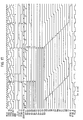
- Fig. 2 shows the phase relation among binary signals DRF-a, DRF-b and DRF-c obtained when the DC reference voltage varies as a, b and c.
- the DRF-a indicates the output waveform when the actual DC reference voltage becomes higher than the optimum DC reference voltage. This output waveform (DRF-a) leading edge is delayed, and the trailing edge is advanced.
- the present invention seeks to provide a digital signal reproducing circuit which can be stably used even with variations in the phase of input signal.
- the present invention seeks further to provide a circuit to reproduce the clock signal and digital signal, without exerting an influence of phase error generated by the vertical error of input signal or DC reference voltage of wave-shaping circuit.
- the present invention seeks further to provide a circuit to detect the phase error of digital signal, and correct it to the proper digital signal by the digital signal processing.
- a digital signal reproducing circuit comprising:
- a digital signal reproducing circuit comprising:
- a digital signal reproducing circuit comprising:
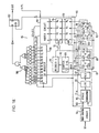
- Fig. 3 shows a digital signal reproducing circuit according to a first embodiment of the present invention.
- signals (RF) containing the EFM modulated digital signal are applied.
- This wave-shaping circuit 16 converts the inputted signals (RF) into binary form.
- These binary signals (DRF) are fed to the phase locked loop circuits (PLL) 17 and 18.
- PLL 17 produces the first bit synchronizing clock (H.PLCK) phase synchronized at the leading edge of binary signal (DRF).
- the PLL 17 produces the data signal A-Da to detect the leading edge of binary signals from the binary signal (DRF) and first bit synchronizing clocks (H.PLCK).
- the PLL 18 produces the second bit synchronizing clock (L.PLCK) phase synchronized at the trailing edge of binary signal (DRF).
- this PLL 18 produces the trailing edge detecting data signal B-Da from the binary signal (DRF) and second bit synchronizing clock (L.PLCK).
- the first and second bit synchronizing clocks are fed to the frequency dividers 19 and 20, respectively.
- the data signals A-Da and B-Da are fed to the pattern detectors 21 and 22, respectively.
- the frequency dividers 19 and 20 divide in four the bit synchronizing clock.
- the outputs of these frequency dividers 19 and 20 are fed to synchronizing circuits 23 and 24, respectively.
- the pattern detectors 21 and 22 detect the time when the binary signal (DRF) becomes the pattern of twice the minimum inversion period or that of twice the maximum inversion period.
- DRF binary signal
- the minimum inversion period of digital signal modulated is of 3T
- its maximum inversion period is of 11T.
- the T is one cycle of the bit synchronizing clock.
- the synchronizing circuits 23 and 24 delay the output signals of frequency dividers 19 and 20, respectively, the output signal of synchronizing circuit 23 is fed to the frequency divider 20, and the output signal of synchronizing (or latch) circuit 24 to the frequency divider 19.
- the frequency dividers 19 and 20 are synchronized.
- the output signal of frequency divider 19 and the output of synchronizing circuit 24 are fed to the timing signal generator 25.
- the output signal of this timing signal generator 25 and the data signals A-Da and H.PLCK outputted from the PLL 17 are fed to the data processor 26.
- This data processor 26 produces digital signals (DOUT) without phase error from these input signals.
- Fig. 4 (a) shows the detailed circuit diagram of PLL 17 in Fig. 3.
- This PLL 17 is composed of a phase comparator 27 to phase compare the binary signal (DRF) and the bit synchronizing clock PLCK, a low pass filter 28 and a VCO 29.
- This phase comparator 27 is composed of two D type flip-flops an AND gate, an OR gate, a P channel MOS FET and an N channel MOS FET, and outputs the leading edge of binary signal (F) and the phase error singal (P-c) of bit synchronizing clock (PLCK).
- This phase error signal (P-c) is fed to the VCO 29 through the low pass filter 28.
- This VCO 29 changes the oscillator frequency of VCO according to the output of low pass filter 28, and outputs the bit synchronizing clock (PLCK).
- This PLL 17 produces first phase error components of binary signal (DRF) and bit synchronizing clock (PLCK).
- the proper phase error is an error detected at the trailing point of time of bit synchronizing clock.
- the phase difference is produced (P-a) first at the leading point of time of binary signal (DRF) and bit synchronizing clock.
- This phase difference signal (P-a) contains off-set components, because the phase difference detection is carried out at the leading point of time of bit synchronizing clock (PLCK).
- the operation of such a PLL 17 can be understood well by the waveform diagram in Fig. 5.
- the PLL 18 in Fig. 3 is a circuit similar to that shown in Fig. 4 (a) with the AND gate and OR gate of the PLL substituted as shown in Fig. 4 (b).
- Fig. 6 shows the binary signal (DRF) and bit synchronizing clocks (H.PLCK and L.PLCK) in the case where the DC reference voltage of wave-shaping circuit varies as levels a, b and c.
- the leading timing phase of binary signal (DRF) is delayed by 1/4 T.
- the phase difference of the 2 bit synchronizing clocks (H.PLCK and L.PLCK) produced in the PLL 17 and 18 is 1/2 T. That is to say, a phase difference of twice the phase error of the binary signal (DRF) is generated. Since the proper digital signal generation is impossible as it is, in the first embodiment, the pattern detector, latch circuit and timing signal generator are utilized.
- Fig. 7 shows a detailed circuit for reproducing detail signals to the first embodiment.
- the PLL 17 is composed of a phase comparator 36 composed of flip-flops 30 and 31, an AND gate 32, and OR gate 33, a P channel MOS gate 34 and an N channel MOS gate 35, a low pass filter 37 and a VCO 38.
- the PLL 18 is composed of a phase comparator 45 composed of flip-flops 39 and 40, a NOR gate 41, a NAND gate 42, a P channel MOS gate 43 and an N channel MOS gate 44, a low pass filter 46 and a VCO 47.
- the frequency divider 19 is composed of flip-flops 48 and 49 and gate circuits 50 and 51.
- the frequency divider 20 is composed of flip-flops 52 and 53 and gate circuits 54 and 55.
- the pattern detector 21 is composed of a counter 56, a NOR gate 57 and an AND gate 58.
- the pattern detector 22 is composed of a counter 59, a NOR gate 60 and an AND gate 61.
- The-synchronizing circuit 23 is composed of flip-flops 62 and 63, and the synchronizing circuit 24 is composed of flip-flops 64 and 65.
- the timing signal generator 25 is composed of a flip-flop 66 and a gate circuit 67.
- the data reproducing circuit 26 is composed of flip-flops 68, 69, 70 and 71.
- the synchronization means contains synchronizing circuits 23 and 24 and gate circuits 50, 51, 54 and 55.
- Fig. 8 is a waveform diagram of this circuit in case the DC reference voltage of wave-shaping circuit 16 is high as indicated by level a in Fig. 6.
- Fig. 9 ⁇ is a waveform diagram of this circuit in case the DC reference voltage of wave-shaping circuit 16 is low as indicated by level c in Fig. 6.
- Binary signals are transmitted to the PLL17 and PLL18.
- the bit synchronizing clock H.PLCK
- the output of NOR gate 57 that is the NOR signal of the Q output of flip-flop 30 and Q output of flip-flop 31, is fed to synchronous clear terminal of counter 56, and as the result this counter 56 is cleared.
- the bit synchronizing clock (L.PLCK) synchronized to the trailing edge of binary signal (DRF) is produced
- the output of NOR gate 60 that is the NOR signal of the Q output of flip-flop 39 and Q output of flip-flop 40
- the pattern detector 21 is to measure the spacing between leading edges of binary signal (DRF)
- the pattern detector 22 is to measure the spacing between trailing edges of binary signal (DRF).
- the counter 56 detects the spacing 6 T between leading edges (the T is one cycle of bit synchronizing clock), and the counter 59 detects that the spacing between trailing edges is of 6 T.
- This 6T is two times 3 T, which is the minimum inversion period of EFM modulation, the minimum inversion period being the minimum spacing in a variety of spacing from the leading edge till the trailing edge or from the trailing edge till the leading edge of binary signal (DRF), and the minimum inversion spacing of EFM modulation being 3 T.
- the fact that 6 T is detected with this counter 56 means that the binary signal (DRF) inputs continuously 3 T and 3 T, and this binary signal (DRF) shall be inverted just at the center of 6 T. Because the fact that the spacing between leading edges of binary signal is of T means that the binary signal (DRF) is of 111000, and no combination other than this exists.
- the minimum inversion period is of 3 T, 2 T + 4 T and 5 T + 1 T cannot be found.
- the frequency dividers 19 and 20 divide into 4 the H.PLCK and L.PLCK, respectively.
- the output state of flip-flops 48 and 49 of frequency divider 19 is latched to the synchronizing circuit 23 at the time of phase comparison timing that is the leading point of time of H.PLCK after change of binary signal (DRF).
- the output state of flip-flops 52 and 53 of frequency divider 20 is latched to the latch circuit at the time of phase comparison timing that is the leading point of time of L.PLCK, signal (DRF).
- DPF binary signal
- the output of this AND gate 58 becomes "1".
- the output of this AND gate 58 is the output of pattern detector 17.
- the content of synchronizing circuit 24 is preset to the frequency divider 19.
- the fact that in this circuit the output of AND gate that is the output of pattern detector is generated means that the leading edge of binary signal (DRF) is also inputted at the point of time only before 6 T from this time.
- the modulation system used in this embodiment is the EFM modulation, and the minimum inversion period of this modulation system is 3 T. Therefore, the trailing edge of binary signal (DRF) before the point of time that the output of AND gate 58 is generated shall be generated properly before 3 T than the point of time that the output of AND gate 58 is generated. If the leading edge of this binary signal (DRF) is generated before 2 T or 4 T than the period of time that the output of AND gate 58 is generated, this is due to an RF signal level variation or a DC reference voltage error.
- a time lag of 1 T is generated from the timing of the leading edge of output pulse of AND gate 58 until the data are set to the flip-flops 48 and 49. Therefore, in terms of the data processing, the time spacing between the leading edge generating point of time of binary signal and the next leading edge seen by the output of frequency divider is 4 T.
- the frequency divider divides into 4 the bit synchronizing clock (1 cycle is of 1 T)
- the time difference of 4 T is therefore the time of 1 cycle of frequency divider. Therefore, the data of the two series are synchronized, by setting the data latched to the flip-flops 64 and 65 to the flip-flops 48 and 49 at the trailing edge timing of AND gate 58.
- the leading edge output timing is the timing delayed in the portion of 2 T at the point of time that the data of flip-flops 64 and 65 agree with the data of flip-flops 48 and 49.
- the outputs of flip-flop 48 and 49 are set at a timing delayed by two bits. This relation is shown in the following table.
- each Q output of flip-flops 69 and 70 is fed to the flip-flop 71, and the digital signal corrected and made with bit synchronization from the Q of this flip-flop is outputted.
- the signal made with EFM modulation is used, however, if it is a question of the signal modulated by the digital modulation system that the minimum inversion period or the maximum inversion period is determined, any signal may be convenient. Moreover, the pattern detector in this embodiment may be changed so as to detect 2 times the maximum inversion period.
- Figs. 10 and 11 show other embodiments of the circuit of the present invention. Most of the elements of this circuit are similar to those found in Figs. 3 and 7, and accordingly have the same numerical designation.
- binary signals made by the wave-shaping circuit 16 are fed to the PLL 17 to be phase synchronized at the leading edge and to the PLL 18 to be phase synchronized at the trailing edge.
- the pattern detector 21 detects that the spacing between leading edges of binary signal is the specified spacing. After the detection signal is obtained by this pattern detector 21,.output signals of frequency divider 19 and frequency divider 20 are synchronized.
- the timing signal generator 25 and the data reproducing circuit 26 detect the phase error in the binary signal, and produce corrected digital signals.
- Fig. 10 and 11 show other embodiments of the circuit of the present invention. Most of the elements of this circuit are similar to those found in Figs. 3 and 7, and accordingly have the same numerical designation.
- binary signals made by the wave-shaping circuit 16 are fed to the PLL 17 to be phase synchronized at the
- the first phase locked circuit means is composed of a phase comparator 36, a low pass filter 37 and a VCO 38
- the second phase locked loop circuit means is composed of a phase comparator 45, a low pass fitler 46 and a VCO 47
- the first frequency divider is composed of a flip-flop 48 and a flip-flop 49.
- the pattern detector circuit is composed of a counter 56, a NOR gate 57 and gate 58.
- the synchronization means contains a synchronizing circuit 24, a gate circuit 50 and a gate circuit 51.
- the timing signal generation means is composed of gate circuit 67 and a flip-flop 66
- the data production circuit is composed of flip-flops 68, 69, 70 and 71.
- Fig. 12 is a waveform diagram of this circuit in the case where the DC reference voltage of wave-shaping circuit 16 is high, as shown by a in Fig. 6.
- Fig. 13 is a waveform diagram of this circuit in case the DC reference voltage of wave-shaping circuit 16 is low as shown by c in Fig. 6.
- Binary signals are fed to the PLL 17 and PLL 18.
- the bit synchronizing clock H.PLCK
- the bit synchronizing clock L.PLCK
- the bit synchronizing clock L.PLCK
- the Q output of flip-flop 39 stands for the data signal that is the trailing edge information of DRF signal, and fed to the synchronizing circuit 24 and the timing signal generator 25.
- the pattern detector 21 detects that the spacing between leading edges of binary signal (DRF) is of 6 T. And the signal indicating that 6 T is detected is outputted from the AND gate 58.
- Two (2) bit synchronizing clocks are divided into 4 by the frequency divider 19 and the frequency divider 20, respectively.
- Each Q output of flip-flops 52 and 53 in this frequency divider 20 is latched to a latch circuit constituted by flip-flops 64 and 65 in the synchronizing circuit 24 at the phase comparison timing.
- the data of 2 series are synchronized by setting the data latched to the flip-flops 64 and 65 to the flip-flops 48 and 49 at the trailing edge timing of AND gate 58.
- the timing difference on actual operation between flip-flops 48 and 49 and flip-flops 64 and 65 is to correspond to the phase difference by DC reference voltage level variation.
- Fig. 13 is a waveform diagram when delaying 1.25 T, because the phase of binary signal (DRF) is in error.
- Fig. 14 shows a block diagram of third embodiment of the present invention.
- the signal (RF) including the digital signal made with EFM modulation are applied.
- This wave-shaping circuit 16 converts the input signal (RF) into binary form.
- the binary signal (DRF) is fed to the phase locked loop circuit (PLL) 81.
- the PLL 81 produces the bit synchronizing clock (PLCK) phase synchronized by the leading edge of binary signal (DRF). Further, the PLL 81 produces the data signal P-a by the binary signal (DRF) and the bit synchronizing clock (PLCK).
- the pattern detector 82 detects whether there is the signal pattern of twice the minimum inversion period in the binary signal (DRF) or not, and feeds the output signal to the phase error detector 83 when there is this signal pattern.
- This phase error detector 83 detects the phase error of binary signal (DRF) that is produced by the DC reference voltage error. This error quantity is fed to the data reproducing circuit 84.
- the data reproducing circuit 84 corrects the binary signal (DRF) by the time base on the basis of the phase error quantity from the phase error detector 83, synchronizes it, and outputs the digital signal.
- Fig. 15 shows a detail circuit diagram of the third embodiment.
- the PLL 81 is composed of a phase comparator 85, a low pass filter 86, a VCO 87 and a frequency divider 88.
- the VCO 87 outputs the master clock (MCK) with frequency of 4 times the bit synchronizing clock according to the output of low pass filter 86.
- the frequency divider 88 divides into 4 the master clock (MCK), and outputs the bit synchronizing clock (PLCK).
- the pattern detector 82 is composed of a counter 89, a decoder 90 and an AND gate 91.
- the phase error detector 83 is composed of frequency dividers 88 and 92, registers 93 and 94 and a NOR gate 103. In this circuit, the frequency divider 88 combinedly uses the frequency divider in the PLL 81.
- the register 93 sets each output data of flip-flops 95, 96, 97 and 98 at the timing of trailing edge of binary signal (DRF).
- the register sets the data of resistor 93 after the spacing between leading edges of binary signal becomes 6 T by means of the pattern detector 82.
- the flip-flops 97 and 98 in this phase error detector 83 are of the circuit configuration shown in Fig. 16.
- the data processor 84 is composed of a matrix circuit 99, a register 100, a gate circuit 101 and a flip-flop 102.
- the relation between the input data and the output data of this matrix circuit 99 is set as shown in the following table.
- the register 100 and gate circuit 101 convert the binary signal (DRF) into the digital signal corrected, on the basis of the control data outputted from the matrix circuit 99.
- the phase comparator 85 outputs the data signal P-a containing the phase difference information from the binary signal (DRF) and bit synchronizing signal.
- This data signal P-a is shown in Fig. 5.
- This data signal P-a clears the flip-flops 97 and 98 and counter 89.
- the output data of flip-flops 95, 96, 97.and 98 are set to the register 93.
- the spacing direction value between bipolar edges of binary signal (DRF) in the pattern detector 82 is possible to change this embodiment to detect two times the maximum inversion period in the digital signal to be inputted. Also, this corrected digital signal is synchronized, and outputted to the bit synchronizing clock (PLCK) by the flip-flop 102.
- Fig. 18 shows a modification of the third embodiment which carries out the phase comparison timing of binary signal (DRF) and bit synchronizing signal (PLCK) and the timing of trailing edge of binary signal (DRF).
- DPF binary signal
- PLCK bit synchronizing signal
- the circuit of Fig. 18 is different from the third embodiment as shown in Fig. 15 in that the inverter 104 is removed from the circuit of Fig. 15 and another inverter 105 is placed between the wave-shaping circuit 16 and the phase comparator 85.
- the rest of the circuit shown in Fig. 18 is the same as the circuit shown in Fig. 15. Therefore it operates identically with the circuit of Fig. 15.
Landscapes
- Engineering & Computer Science (AREA)
- Signal Processing (AREA)
- Signal Processing For Digital Recording And Reproducing (AREA)
- Stabilization Of Oscillater, Synchronisation, Frequency Synthesizers (AREA)
- Synchronisation In Digital Transmission Systems (AREA)
Claims (22)
Applications Claiming Priority (6)
| Application Number | Priority Date | Filing Date | Title |
|---|---|---|---|
| JP60066891A JPS61227270A (ja) | 1985-03-30 | 1985-03-30 | デ−タストロ−ブ回路 |
| JP60066893A JPS61227271A (ja) | 1985-03-30 | 1985-03-30 | デ−タストロ−ブ回路 |
| JP66891/85 | 1985-03-30 | ||
| JP66893/85 | 1985-03-30 | ||
| JP66890/85 | 1985-03-30 | ||
| JP60066890A JPS61227269A (ja) | 1985-03-30 | 1985-03-30 | デ−タストロ−ブ回路 |
Publications (2)
| Publication Number | Publication Date |
|---|---|
| EP0200370A1 EP0200370A1 (fr) | 1986-11-05 |
| EP0200370B1 true EP0200370B1 (fr) | 1990-06-13 |
Family
ID=27299296
Family Applications (1)
| Application Number | Title | Priority Date | Filing Date |
|---|---|---|---|
| EP86302388A Expired - Lifetime EP0200370B1 (fr) | 1985-03-30 | 1986-04-01 | Circuit de reproduction de signaux numériques |
Country Status (4)
| Country | Link |
|---|---|
| US (1) | US4713802A (fr) |
| EP (1) | EP0200370B1 (fr) |
| KR (1) | KR900001593B1 (fr) |
| DE (1) | DE3672003D1 (fr) |
Families Citing this family (18)
| Publication number | Priority date | Publication date | Assignee | Title |
|---|---|---|---|---|
| JPS63138506A (ja) * | 1986-11-29 | 1988-06-10 | Toshiba Corp | フロツピ−デイスク装置のデ−タ再生回路 |
| US4872155A (en) * | 1987-03-13 | 1989-10-03 | Pioneer Electronic Corporation | Clock generator circuit and a synchronizing signal detection method in a sampled format system and a phase comparator circuit suited for generation of the clock |
| US4823209A (en) * | 1987-11-05 | 1989-04-18 | Magnetic Peripherals Inc. | 1,7,2,3 Encoding/decoding employing 3/2 frequency division |
| JPH01269280A (ja) * | 1988-04-20 | 1989-10-26 | Sony Corp | 光デイスク装置 |
| JP2589759B2 (ja) * | 1988-05-27 | 1997-03-12 | 松下電器産業株式会社 | データ識別装置 |
| JPH01317281A (ja) * | 1988-06-16 | 1989-12-21 | Pioneer Electron Corp | 記録データ再生装置 |
| JPH0220802U (fr) * | 1988-07-26 | 1990-02-13 | ||
| US5132957A (en) * | 1988-11-07 | 1992-07-21 | Teac Corporation | Information signal recording and reproducing system capable of recording an information signal on a medium having a limited recording band width |
| EP0420667B1 (fr) * | 1989-09-29 | 1997-08-06 | Kabushiki Kaisha Toshiba | Régulateur de phase synchrone pour la production d'un signal d'horloge de référence dans un système d'entraînement de disques |
| JPH0834046B2 (ja) * | 1989-10-26 | 1996-03-29 | 日本ビクター株式会社 | データ検出用信号発生回路 |
| US5333126A (en) * | 1990-01-03 | 1994-07-26 | Hitachi, Ltd. | Information recording method and optical disk apparatus using same |
| EP0500263A3 (en) * | 1991-02-20 | 1993-06-09 | Research Machines Plc | Method for synchronising a receiver's data clock |
| JPH06162668A (ja) * | 1992-11-24 | 1994-06-10 | Hitachi Ltd | 情報記録方式 |
| US5365382A (en) * | 1993-05-18 | 1994-11-15 | Digital Equipment Corporation | Synchronization to different fields in a storage device |
| US6067335A (en) * | 1996-08-02 | 2000-05-23 | Silicon Systems, Inc. | Read channel IC for dual PLL solution |
| JP3363712B2 (ja) | 1996-08-06 | 2003-01-08 | 株式会社リコー | 光ディスク装置 |
| US5986592A (en) * | 1996-10-01 | 1999-11-16 | Sony Corporation | Encoder decoder device not using an A/D converter and method thereof |
| US7532695B2 (en) * | 2002-10-10 | 2009-05-12 | Infineon Technologies Ag | Clock signal extraction device and method for extracting a clock signal from data signal |
Family Cites Families (5)
| Publication number | Priority date | Publication date | Assignee | Title |
|---|---|---|---|---|
| JPS5813046A (ja) * | 1981-07-17 | 1983-01-25 | Victor Co Of Japan Ltd | デ−タ読み取り回路 |
| US4611335A (en) * | 1981-09-30 | 1986-09-09 | Hitachi, Ltd. | Digital data synchronizing circuit |
| SE425149B (sv) * | 1981-10-29 | 1982-09-06 | Isoflex Ab | Anordning for kontinuerlig veckning eller korrugering av ett banformigt material i dess lengdriktning |
| US4583211A (en) * | 1982-06-15 | 1986-04-15 | Tokyo Shibaura Denki Kabushiki Kaisha | Frequency detecting circuit for digital information reproducing system |
| JPS58220226A (ja) * | 1982-06-15 | 1983-12-21 | Toshiba Corp | 位相ロツクル−プ制御回路 |
-
1986
- 1986-03-21 KR KR1019860002124A patent/KR900001593B1/ko not_active Expired
- 1986-03-31 US US06/846,208 patent/US4713802A/en not_active Expired - Lifetime
- 1986-04-01 EP EP86302388A patent/EP0200370B1/fr not_active Expired - Lifetime
- 1986-04-01 DE DE8686302388T patent/DE3672003D1/de not_active Expired - Lifetime
Also Published As
| Publication number | Publication date |
|---|---|
| EP0200370A1 (fr) | 1986-11-05 |
| KR900001593B1 (ko) | 1990-03-15 |
| DE3672003D1 (de) | 1990-07-19 |
| US4713802A (en) | 1987-12-15 |
| KR860007659A (ko) | 1986-10-15 |
Similar Documents
| Publication | Publication Date | Title |
|---|---|---|
| EP0200370B1 (fr) | Circuit de reproduction de signaux numériques | |
| US4777542A (en) | Data recording method | |
| KR860001260B1 (ko) | 디지탈 변조신호 판독장치에 있어서의 클록 발생용 pll의 록 검출 방식 | |
| JPH0765512A (ja) | 再生クロック生成回路 | |
| JPS5977605A (ja) | 読取りクロツク生成方式 | |
| US6580775B1 (en) | Method of detecting frequency of digital phase locked loop | |
| US4580100A (en) | Phase locked loop clock recovery circuit for data reproducing apparatus | |
| KR960035239A (ko) | 디코드장치 및 기억장치 | |
| JPS59167813A (ja) | 位相同期回路 | |
| CA1162618A (fr) | Circuit de synchronisation de phase | |
| JP2636349B2 (ja) | 位相制御回路 | |
| JPS61227271A (ja) | デ−タストロ−ブ回路 | |
| JPS61227270A (ja) | デ−タストロ−ブ回路 | |
| JP3123612B2 (ja) | 時間軸補正装置 | |
| JPS61225926A (ja) | デジタルロジツクpll回路 | |
| JP2529325B2 (ja) | スライス回路 | |
| JPS61227269A (ja) | デ−タストロ−ブ回路 | |
| JPH0710113B2 (ja) | 位相同期クロツク信号発生装置 | |
| JPH07111046A (ja) | 光ディスク装置のデータ再生回路 | |
| JPS5989052A (ja) | ビツト同期回路 | |
| JPH0281324A (ja) | 再生信号補正方法 | |
| JPS61236072A (ja) | 信号同期回路 | |
| JPH0294916A (ja) | データスライス回路 | |
| JPH0834039B2 (ja) | ディジタル信号処理装置 | |
| JPS5944144A (ja) | 同期信号発生装置 |
Legal Events
| Date | Code | Title | Description |
|---|---|---|---|
| PUAI | Public reference made under article 153(3) epc to a published international application that has entered the european phase |
Free format text: ORIGINAL CODE: 0009012 |
|
| 17P | Request for examination filed |
Effective date: 19860415 |
|
| AK | Designated contracting states |
Kind code of ref document: A1 Designated state(s): DE FR GB NL |
|
| 17Q | First examination report despatched |
Effective date: 19881014 |
|
| GRAA | (expected) grant |
Free format text: ORIGINAL CODE: 0009210 |
|
| AK | Designated contracting states |
Kind code of ref document: B1 Designated state(s): DE FR GB NL |
|
| REF | Corresponds to: |
Ref document number: 3672003 Country of ref document: DE Date of ref document: 19900719 |
|
| ET | Fr: translation filed | ||
| PLBE | No opposition filed within time limit |
Free format text: ORIGINAL CODE: 0009261 |
|
| STAA | Information on the status of an ep patent application or granted ep patent |
Free format text: STATUS: NO OPPOSITION FILED WITHIN TIME LIMIT |
|
| 26N | No opposition filed | ||
| PGFP | Annual fee paid to national office [announced via postgrant information from national office to epo] |
Ref country code: NL Payment date: 20000428 Year of fee payment: 15 |
|
| PG25 | Lapsed in a contracting state [announced via postgrant information from national office to epo] |
Ref country code: NL Free format text: LAPSE BECAUSE OF NON-PAYMENT OF DUE FEES Effective date: 20011101 |
|
| REG | Reference to a national code |
Ref country code: GB Ref legal event code: IF02 |
|
| NLV4 | Nl: lapsed or anulled due to non-payment of the annual fee |
Effective date: 20011101 |
|
| PGFP | Annual fee paid to national office [announced via postgrant information from national office to epo] |
Ref country code: DE Payment date: 20050324 Year of fee payment: 20 |
|
| PGFP | Annual fee paid to national office [announced via postgrant information from national office to epo] |
Ref country code: GB Payment date: 20050330 Year of fee payment: 20 |
|
| PGFP | Annual fee paid to national office [announced via postgrant information from national office to epo] |
Ref country code: FR Payment date: 20050408 Year of fee payment: 20 |
|
| PG25 | Lapsed in a contracting state [announced via postgrant information from national office to epo] |
Ref country code: GB Free format text: LAPSE BECAUSE OF EXPIRATION OF PROTECTION Effective date: 20060331 |
|
| REG | Reference to a national code |
Ref country code: GB Ref legal event code: PE20 |