EP0194199A2 - Thyristor à induction statique à double porte et son procédé de fabrication - Google Patents
Thyristor à induction statique à double porte et son procédé de fabrication Download PDFInfo
- Publication number
- EP0194199A2 EP0194199A2 EP86400432A EP86400432A EP0194199A2 EP 0194199 A2 EP0194199 A2 EP 0194199A2 EP 86400432 A EP86400432 A EP 86400432A EP 86400432 A EP86400432 A EP 86400432A EP 0194199 A2 EP0194199 A2 EP 0194199A2
- Authority
- EP
- European Patent Office
- Prior art keywords
- substrate
- epitaxial
- type
- gate
- layer
- Prior art date
- Legal status (The legal status is an assumption and is not a legal conclusion. Google has not performed a legal analysis and makes no representation as to the accuracy of the status listed.)
- Granted
Links
- 230000006698 induction Effects 0.000 title claims abstract description 27
- 230000003068 static effect Effects 0.000 title claims abstract description 27
- 238000000034 method Methods 0.000 title claims description 33
- 238000004519 manufacturing process Methods 0.000 title claims description 16
- 239000000758 substrate Substances 0.000 claims abstract description 86
- 239000004065 semiconductor Substances 0.000 claims abstract description 49
- 239000012535 impurity Substances 0.000 claims description 33
- XUIMIQQOPSSXEZ-UHFFFAOYSA-N Silicon Chemical compound [Si] XUIMIQQOPSSXEZ-UHFFFAOYSA-N 0.000 claims description 22
- 229910052710 silicon Inorganic materials 0.000 claims description 22
- 239000010703 silicon Substances 0.000 claims description 22
- 239000000463 material Substances 0.000 claims description 10
- 238000000151 deposition Methods 0.000 claims description 6
- 238000005530 etching Methods 0.000 claims description 6
- 229910021332 silicide Inorganic materials 0.000 claims description 6
- VLJQDHDVZJXNQL-UHFFFAOYSA-N 4-methyl-n-(oxomethylidene)benzenesulfonamide Chemical compound CC1=CC=C(S(=O)(=O)N=C=O)C=C1 VLJQDHDVZJXNQL-UHFFFAOYSA-N 0.000 claims description 3
- 229910021340 platinum monosilicide Inorganic materials 0.000 claims description 3
- 230000015572 biosynthetic process Effects 0.000 claims description 2
- 229910052697 platinum Inorganic materials 0.000 claims description 2
- FVBUAEGBCNSCDD-UHFFFAOYSA-N silicide(4-) Chemical compound [Si-4] FVBUAEGBCNSCDD-UHFFFAOYSA-N 0.000 claims description 2
- 239000004020 conductor Substances 0.000 claims 1
- 229910052751 metal Inorganic materials 0.000 description 8
- 239000002184 metal Substances 0.000 description 8
- 239000013078 crystal Substances 0.000 description 5
- OAICVXFJPJFONN-UHFFFAOYSA-N Phosphorus Chemical compound [P] OAICVXFJPJFONN-UHFFFAOYSA-N 0.000 description 4
- 150000002739 metals Chemical class 0.000 description 4
- 229910052698 phosphorus Inorganic materials 0.000 description 4
- 239000011574 phosphorus Substances 0.000 description 4
- 230000007547 defect Effects 0.000 description 3
- 238000009792 diffusion process Methods 0.000 description 3
- 238000005516 engineering process Methods 0.000 description 3
- 239000000969 carrier Substances 0.000 description 2
- 150000002500 ions Chemical class 0.000 description 2
- 229910016006 MoSi Inorganic materials 0.000 description 1
- 238000000137 annealing Methods 0.000 description 1
- 238000010276 construction Methods 0.000 description 1
- 238000001312 dry etching Methods 0.000 description 1
- 238000010438 heat treatment Methods 0.000 description 1
- 238000005468 ion implantation Methods 0.000 description 1
- 238000012986 modification Methods 0.000 description 1
- 230000004048 modification Effects 0.000 description 1
- 230000002093 peripheral effect Effects 0.000 description 1
Images


Classifications
-
- H—ELECTRICITY
- H01—ELECTRIC ELEMENTS
- H01L—SEMICONDUCTOR DEVICES NOT COVERED BY CLASS H10
- H01L29/00—Semiconductor devices specially adapted for rectifying, amplifying, oscillating or switching and having potential barriers; Capacitors or resistors having potential barriers, e.g. a PN-junction depletion layer or carrier concentration layer; Details of semiconductor bodies or of electrodes thereof ; Multistep manufacturing processes therefor
- H01L29/66—Types of semiconductor device ; Multistep manufacturing processes therefor
- H01L29/68—Types of semiconductor device ; Multistep manufacturing processes therefor controllable by only the electric current supplied, or only the electric potential applied, to an electrode which does not carry the current to be rectified, amplified or switched
- H01L29/70—Bipolar devices
- H01L29/72—Transistor-type devices, i.e. able to continuously respond to applied control signals
- H01L29/739—Transistor-type devices, i.e. able to continuously respond to applied control signals controlled by field-effect, e.g. bipolar static induction transistors [BSIT]
- H01L29/7391—Gated diode structures
- H01L29/7392—Gated diode structures with PN junction gate, e.g. field controlled thyristors (FCTh), static induction thyristors (SITh)
-
- H—ELECTRICITY
- H01—ELECTRIC ELEMENTS
- H01L—SEMICONDUCTOR DEVICES NOT COVERED BY CLASS H10
- H01L29/00—Semiconductor devices specially adapted for rectifying, amplifying, oscillating or switching and having potential barriers; Capacitors or resistors having potential barriers, e.g. a PN-junction depletion layer or carrier concentration layer; Details of semiconductor bodies or of electrodes thereof ; Multistep manufacturing processes therefor
- H01L29/02—Semiconductor bodies ; Multistep manufacturing processes therefor
- H01L29/06—Semiconductor bodies ; Multistep manufacturing processes therefor characterised by their shape; characterised by the shapes, relative sizes, or dispositions of the semiconductor regions ; characterised by the concentration or distribution of impurities within semiconductor regions
- H01L29/10—Semiconductor bodies ; Multistep manufacturing processes therefor characterised by their shape; characterised by the shapes, relative sizes, or dispositions of the semiconductor regions ; characterised by the concentration or distribution of impurities within semiconductor regions with semiconductor regions connected to an electrode not carrying current to be rectified, amplified or switched and such electrode being part of a semiconductor device which comprises three or more electrodes
- H01L29/1066—Gate region of field-effect devices with PN junction gate
Definitions
- the present invention relates to a buried-gate type double gate static induction thyristor, and more specifically to an easily fabricable double gate static induction thyristor and a manufacturing method therefor.
- the double gate static induction thyristors have already proposed and examined by various publications such as Japanese patent publication No. 4100/1982, U.S. patent No. 4 086 611 and the Trans. Electron Devices, vol. ED-22, No. 4, pp 185-195 (1975).
- This double gate static induction thyristor can not only switch a large current at a very high speed, but also can be turned off by controlling the voltage of the gate, differently from conventional silicon controlled rectifiers.
- Figure 1 shows a schematic cross-sectional view of a typical example of the double gate static induction thyristors.
- the shown thyristor is separated into an upper part and a lower part by a center p-n junction 26.
- the upper part includes a p -type semiconductor layer 25 contiguous to an n - -type semiconductor layer 24 of the lower part so as to form the p-n junction 26 therebetween.
- Another p - -type semiconductor layer 29 is formed on the layer 25, and in addition, n -type gate regions 27 are formed at a periphery of the layer 25 and also between the layers 25 and 29 in the form of buried regions.
- An anode electrode 30 is deposited on the second p - -type layer 29.
- a second n - -type semiconductor layer 21 is formed on the first n - -type layer 24, and p +- type gate regions 22 are formed at a periphery of the layer 24 and also between the layers 21 and 24 in the form of buried regions.
- a cathode electrode 31 is deposited on the second n - -type layer 21, and gate electrodes 32 are deposited on the exposed gate regions 22 and 27.
- the term "p - -type” is used to mean that p-type impurities are included or doped at a low concentration
- the "p +- type” is used to mean that p-type impurities are included or doped at a high concentration.
- the "n - -type” means that n-type impurities are included or doped at a low concentration
- the "n +- type” means that n-type impurities are included or doped at a high concentration.
- the conventional double gate static induction thyristor is characterized in that the p +- type first gate region 22 and the n +- type second gate region 27 are separated on both sides on the p-n junction 26.
- a semiconductor substrate is prepared to constitute the n - -type semiconductor layer 21. Then, the following operations are sequentially performed to the substrate 21:
- the p - -type semiconductor lower layer 23 is provided by a substrate. Then, the following operations are sequentially performed to the substrate 25:
- the conventional double gate static induction thyristors have a plurality of superposed or stacked epitaxial layers which require the highly controlled crystal growth technology. Therefore, it has heretofore been difficult to manufacture double gate static induction thyristors on a mass-production basis. Accordingly, although the double gate static induction thyristors have been recognized to be more excellent than the conventional thyristors, they could not have been widely used in practice.
- Another object of the present invention is to provide a double gate static induction thyristor in which only one epitaxial layer is deposited on each principal surface of a semi-conductor substrate.
- Still another object of the present invention is to provide a method for manufacturing the above double gate static induction thyristor, which method does not require to stack a plurality of epitaxial layers to each other.
- a double gate static induction thyristor comprising a semiconductor substrate of a given conduction type having first and second principal surfaces opposite to each other, a first epitaxial semiconductor layer of a first conduction type formed on the first principal surface of the substrate, a second epitaxial semiconductor layer of a second conduction type opposite to the first conduction type and formed on the second principal surface of the substrate, a cathode electrode deposited on the surface of the first epitaxial layer, an anode electrode deposited on the surface of the second epitaxial layer, a first gate electrode formed on the first principal surface of the substrate, and a second gate electrode formed on the second principal surface of the substrate.
- the substrate has a first gate region formed in the first principal surface and having the second conduction type, and a second gate region formed in the second principal surface and having the first conduction type.
- the above first and second gate electrodes are formed on the first and second gate regions, respectively.
- first and second epitaxial layers have highly doped surface regions, respectively, and the cathode and anode main electrodes are respectively deposited on the highly doped surface regions of the first and second epitaxial layers.
- the substrate is an n-type silicon substrate, and the first conduction type is n-type and the second conduction type is p-type.
- the substrate may be a p-type silicon substrate.
- the anode electrode and the first gate electrode are formed of a material having a work function larger than that of the associated semiconductor regions
- the cathode electrode and the second gate electrode are formed of a material having a work function smaller than that of the associated semiconductor regions.
- the anode electrode and the first gate electrode are formed of a material selected from a group consisting of Pt and PtSi
- the cathode electrode and the second gate electrode are formed of a material selected from a group consisting of Al, Ti, Mo and their silicide.
- the substrate has the thickness of about 400-450 micrometers and the impurity concentration of 1 x 10 13 to 2 x 10 13 cm -3
- the first and second gate regions are respectively formed in the first and second principal surfaces of the substrate to have the depth of 15 to 20 micrometers and the surface impurity concentration of 1 x 10 18 to 1 x 10 19 cm -3
- the first and second epitaxial layers are respectively formed on the first and second principal surfaces to have the thickness of about 30 micrometers at a relatively low impurity concentration.
- the first and second epitaxial layers respectively have a first layer of about 1.5 micrometer thickness formed on the substrate to have a resistivity of 180 milliohms-centimeter, and a second layer of about 28.5 micrometer thickness formed on the first layer to have a resistivity of 20 ohms-centimeter.
- the highly doped surface region formed on each of the first and second epitaxial layers has a thickness of 7 micrometers and a surface impurity concentration of not less than 5 x 10 19 cm- 3 .
- the above mentioned double gate static induction thyristor can be manufactured by a method in accordance with the present invention, which comprises the steps of:
- first and second gate regions are selectively formed in the first and second principal surfaces of the substrate, respectively, and the first and second gate electrodes are deposited on the first and second gate regions, respectively.
- the first epitaxial layer is formed by the steps of depositing a first semiconductor layer of the first conduction type on the first principal surface of the substrate by means of an epitaxial growth process, and selectively removing the first epitaxial layer by an etching process to cause the first gate region to be exposed.
- the second epitaxial layer is formed by the step of depositing a second semiconductor layer of the second conduction type on the second principal surface by means of an epitaxial growth process, and selectively removing the second epitaxial layer by an etching process to cause the second gate region to be exposed.
- the surface of the first and second epitaxial layers are strongly doped by impurities of the first and second conduction types, respectively, and the cathode and anode electrodes are deposited on the strongly doped surfaces of the first and second epitaxial layers, respectively:
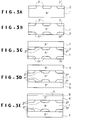
- the shown thyristor comprises an n - -type silicon substrate 1, which has first gate regions 2 of p +- type selectively formed in an upper principal surface thereof and second gate regions 3 of n + -type also selectively formed in a lower principal surface of the substrate.
- epitaxial silicon layers 4 of n - -type are selectively formed on the upper principal surface of the substrate 1 so as to overlie on a periphery of the first gate regions 2 and also, epitaxial silicon layer 5 of p - -type are selectively formed on the lower principal surface of the substrate 1 so as to overlap on a peripheral portion of the second gate regions 3.
- first and second gate electrodes 10 and 11 are formed on the exposed surfaces of the first and second gate regions 2 and 3.
- the epitaxial layer 4 is formed on the upper principal surface of the substrate 1 and the epitaxial layer 5 is formed on the lower principal surface of the substrate 1. Namely, the two epitaxial layers 4 and 5 do not lie on each other. Therefore, since there is not required a highly controlled epitaxial growth technique for stacking a plurality of epitaxial layers, the above thyristor can be easily manufactured by the ordinary epitaxial growth technique.
- figure 2B there is another embodiment of the thyristor in accordance with the present invention, in which a p--type silicon substrate 12 is used in place of the n-type substrate 1 in the first embodiment shown in figure 2A.
- the second embodiment of figure 2B is the same as that of figure 2A.
- a n - -type silicon substrate 1 having a thickness of about 400-450 micrometers and an impurity concentration of 1 x 10 13 to 2 x 10 13 cm -3 is prepared, and then, p + -type first gate regions 2 is formed partially on an upper principal surface, or the first surface, of the n - -type silicon substrate 1 by selectively doping p-type impurities such borons at a high concentration.
- n -type second gate regions 3 is formed partially on a lower principal surface, or the second surface, of the n-type silicon substrate I by selectively doping n-type impurities such as phosphorus at a high concentration.
- These gate regions 2 and 3 thus formed have the surface impurity concentration ranging for example from 1 x 10 18 to 1 x 10 19 cm -3 and the depth in the range of 15 of 20 micrometers.
- the above selective doping of impurities was performed by means of an ion implantation method and by using a suitable mask formed on the surface of the substrate and provided with necessary windows. If the substrate is left as it is after ions are implanted, the substrate shows very high surface specific resistivity, because defects appear in the substrate and most implanted ions do not yet become carriers. Therefore, in order to disappear defects and to change impurities into carriers, an annealing operation is performed. In the present case, the substrate is heated at first at about 500°C. Thereafter, the substrate is driven in at about 1200°C so as to cause a high temperature diffusion, and then gradually cooled to nearly 560°C.
- An alternative for impurity doping is a gas diffusion method.
- an oxide layer is first formed on the surface of the substrate.
- gate region windows are formed, which will be a diffusion mask.
- the substrate is heated in an atmosphere including impurities atoms, so that the impurities diffuse in the substrate through the windows to selectively form the gate regions.
- an n -type silicon region 4 containing a low concentration of n-type impurities such as phosphorus is epitaxially grown on the first or upper surface of the substrate 1.
- the thickness of this n - -type epitaxial layer 4 is about 30 micrometers.
- the epitaxial growth of the layer 4 is divided into two steps so as to suppress autodoping or outdiffusion from the gate regions 2 to the epitaxial layer 4: first, a first n-type silicon layer having a specific resistivity of 180 milliohms-centimeter is grown directly on the substrate 1 in about 1.5 micrometer thickness by means of a high impurity concentration epitaxial growth; and then, a second n-type silicon layer of a specific resistivity in the range of 10 to 20 ohms-centimeter is grown with a thickness of about 28.5 micrometers by means of a low impurity concentration epitaxial growth.
- low pressure epitaxial growth method with lamp heating was preferably used.
- a p--type silicon region 5 doped with p-type impurities such as borons at a low concentration is epitaxially grown on the second or lower surface of the substrate 1.
- the thickness of this p - -type epitaxial layer 5 is about 30 micrometers.
- This epitaxial growth also proceeds in two steps just as has been done above; first, a first p-type silicon layer having a specific resistivity of 180 milliohms-centimeter is grown directly on the substrate 1 with about 1.5 micrometer thickness by a high impurity concentration epitaxial growth; and then, a second p-type silicon layer of a specific resistivity of 10 to 20 ohms-centimeter is grown at about 28.5 micrometer by a low impurity concentration epitaxial growth.
- an n + -type silicon layer 6 is formed on the entire surface of the n - -type epitaxial layer 4 by doping n-type impurities such as phosphorus into the surface region of the epitaxial layer 4 so as to have, for example, an impurity concentration of not less than 5 x 10 19 cm -3 and the thickness of 7 micrometers.
- an p + -type silicon layer 7 is formed on the entire surface of the p - -type epitaxial layer 5 by doping n-type impurities such as phosphorus with an impurity concentration of not less than 5 x 10 19 cm -3 and in the thickness of 7 micrometers.
- n - -type epitaxial layer 4 and the n -type surface region 6 are etched to expose the p +- type first gate regions 2.
- a part of the p - -type epitaxial layer 5 and the p +- type surface region 7 are etched to expose the p +- type second gate regions 3.
- cathode electrodes 8, first gate electrodes 10, anode electrodes 9 and second gate electrodes 11 are formed on the n +- type surface regions 6, the p +- type first gate regions 2, the p +- type surface regions 7 and the n + -type first gate regions 3, respectively.
- metals or metal silicides such as Pt, PtSi, etc. having a work function larger than the silicon.
- metals or metal silicides such as Al, Ti, Mo, MoSi, etc. having a work function smaller than the silicon are preferably used as the material for the cathode electrode 8 and the second gate electrode 11.
- Concerning electrodes not only metals or metal silicides themselves, but also multi layered structure of two or more kinds of metals or metal silicides may be used.
- the thyristor according to the present invention has an advantage that the structure is simpler than that of the prior art. Another advantage is found in the manufacturing method in which epitaxial growth layers are not superposed. Therefore, no specific crystal growth technique is required, resulting in the possibility of applying the technique in the prior art in manufacturing the thyristor according to the invention.
Landscapes
- Engineering & Computer Science (AREA)
- Microelectronics & Electronic Packaging (AREA)
- Power Engineering (AREA)
- Physics & Mathematics (AREA)
- Ceramic Engineering (AREA)
- Condensed Matter Physics & Semiconductors (AREA)
- General Physics & Mathematics (AREA)
- Computer Hardware Design (AREA)
- Thyristors (AREA)
Applications Claiming Priority (2)
| Application Number | Priority Date | Filing Date | Title |
|---|---|---|---|
| JP60039378A JPS61198779A (ja) | 1985-02-28 | 1985-02-28 | 両面ゲ−ト静電誘導サイリスタ及びその製造方法 |
| JP39378/85 | 1985-03-19 |
Publications (3)
| Publication Number | Publication Date |
|---|---|
| EP0194199A2 true EP0194199A2 (fr) | 1986-09-10 |
| EP0194199A3 EP0194199A3 (en) | 1986-12-17 |
| EP0194199B1 EP0194199B1 (fr) | 1990-05-30 |
Family
ID=12551359
Family Applications (1)
| Application Number | Title | Priority Date | Filing Date |
|---|---|---|---|
| EP86400432A Expired EP0194199B1 (fr) | 1985-02-28 | 1986-02-28 | Thyristor à induction statique à double porte et son procédé de fabrication |
Country Status (4)
| Country | Link |
|---|---|
| US (2) | US4837608A (fr) |
| EP (1) | EP0194199B1 (fr) |
| JP (1) | JPS61198779A (fr) |
| DE (1) | DE3671680D1 (fr) |
Cited By (2)
| Publication number | Priority date | Publication date | Assignee | Title |
|---|---|---|---|---|
| EP0239866A1 (fr) * | 1986-03-20 | 1987-10-07 | BBC Aktiengesellschaft Brown, Boveri & Cie. | Elément semi-conducteur à extinction ainsi que son utilisation |
| GB2230136A (en) * | 1989-03-28 | 1990-10-10 | Matsushita Electric Works Ltd | Method for manufacturing static induction type semiconductor device |
Families Citing this family (4)
| Publication number | Priority date | Publication date | Assignee | Title |
|---|---|---|---|---|
| JP2577330B2 (ja) * | 1986-12-11 | 1997-01-29 | 新技術事業団 | 両面ゲ−ト静電誘導サイリスタの製造方法 |
| US5318916A (en) * | 1992-07-31 | 1994-06-07 | Research Triangle Institute | Symmetric self-aligned processing |
| US5241195A (en) * | 1992-08-13 | 1993-08-31 | North Carolina State University At Raleigh | Merged P-I-N/Schottky power rectifier having extended P-I-N junction |
| US6690039B1 (en) * | 2002-10-01 | 2004-02-10 | T-Ram, Inc. | Thyristor-based device that inhibits undesirable conductive channel formation |
Citations (3)
| Publication number | Priority date | Publication date | Assignee | Title |
|---|---|---|---|---|
| US4086611A (en) * | 1975-10-20 | 1978-04-25 | Semiconductor Research Foundation | Static induction type thyristor |
| EP0064561A1 (fr) * | 1980-11-21 | 1982-11-17 | Zaidan Hozin Handotai Kenkyu Shinkokai | Tiristor d'induction statique |
| EP0094974A1 (fr) * | 1981-12-01 | 1983-11-30 | Semiconductor Research Foundation | Convertisseur photoelectrique a semi-conducteurs |
Family Cites Families (17)
| Publication number | Priority date | Publication date | Assignee | Title |
|---|---|---|---|---|
| NL96818C (fr) * | 1952-03-14 | |||
| US3274400A (en) * | 1964-01-17 | 1966-09-20 | Int Rectifier Corp | Temperature compensated silicon controlled rectifier |
| CH436492A (de) * | 1965-10-21 | 1967-05-31 | Bbc Brown Boveri & Cie | Steuerbare Halbleitervorrichtung mit mehreren Schichten |
| US3684902A (en) * | 1966-06-07 | 1972-08-15 | Westinghouse Electric Corp | Semiconductor switch device |
| US3953254A (en) * | 1972-11-07 | 1976-04-27 | Thomson-Csf | Method of producing temperature compensated reference diodes utilizing selective epitaxial growth |
| US4171995A (en) * | 1975-10-20 | 1979-10-23 | Semiconductor Research Foundation | Epitaxial deposition process for producing an electrostatic induction type thyristor |
| JPS5250175A (en) * | 1975-10-20 | 1977-04-21 | Semiconductor Res Found | Electrostatic induction type thyristor |
| GB1586171A (en) * | 1977-01-31 | 1981-03-18 | Rca Corp | Gate turn-off device |
| JPS55128870A (en) * | 1979-03-26 | 1980-10-06 | Semiconductor Res Found | Electrostatic induction thyristor and semiconductor device |
| JPS6011815B2 (ja) * | 1979-07-09 | 1985-03-28 | 三菱電機株式会社 | サイリスタ |
| JPS6019150B2 (ja) * | 1979-10-05 | 1985-05-14 | 株式会社日立製作所 | 半導体装置の製造方法 |
| JPS574100A (en) * | 1980-06-10 | 1982-01-09 | Sharp Kk | Voice information output device |
| FR2508703A1 (fr) * | 1981-06-30 | 1982-12-31 | Commissariat Energie Atomique | Diode zener compensee en temperature et stable sous irradiation et procede de fabrication d'une telle diode |
| US4545111A (en) * | 1983-01-18 | 1985-10-08 | Energy Conversion Devices, Inc. | Method for making, parallel preprogramming or field programming of electronic matrix arrays |
| JPS60247969A (ja) * | 1984-05-23 | 1985-12-07 | Toyo Electric Mfg Co Ltd | 自己消弧形半導体素子 |
| JPS61144066A (ja) * | 1984-12-17 | 1986-07-01 | Semiconductor Res Found | 光トリガサイリスタ |
| US4624004A (en) * | 1985-07-15 | 1986-11-18 | Eaton Corporation | Buried channel MESFET with backside source contact |
-
1985
- 1985-02-28 JP JP60039378A patent/JPS61198779A/ja not_active Withdrawn
-
1986
- 1986-02-28 DE DE8686400432T patent/DE3671680D1/de not_active Expired - Fee Related
- 1986-02-28 EP EP86400432A patent/EP0194199B1/fr not_active Expired
-
1988
- 1988-07-14 US US07/219,902 patent/US4837608A/en not_active Expired - Lifetime
-
1989
- 1989-03-12 US US07/322,515 patent/US4870028A/en not_active Expired - Lifetime
Patent Citations (3)
| Publication number | Priority date | Publication date | Assignee | Title |
|---|---|---|---|---|
| US4086611A (en) * | 1975-10-20 | 1978-04-25 | Semiconductor Research Foundation | Static induction type thyristor |
| EP0064561A1 (fr) * | 1980-11-21 | 1982-11-17 | Zaidan Hozin Handotai Kenkyu Shinkokai | Tiristor d'induction statique |
| EP0094974A1 (fr) * | 1981-12-01 | 1983-11-30 | Semiconductor Research Foundation | Convertisseur photoelectrique a semi-conducteurs |
Cited By (3)
| Publication number | Priority date | Publication date | Assignee | Title |
|---|---|---|---|---|
| EP0239866A1 (fr) * | 1986-03-20 | 1987-10-07 | BBC Aktiengesellschaft Brown, Boveri & Cie. | Elément semi-conducteur à extinction ainsi que son utilisation |
| GB2230136A (en) * | 1989-03-28 | 1990-10-10 | Matsushita Electric Works Ltd | Method for manufacturing static induction type semiconductor device |
| GB2230136B (en) * | 1989-03-28 | 1993-02-10 | Matsushita Electric Works Ltd | Method for manufacturing static induction type semiconductor device and semiconductor devices manufactured thereby |
Also Published As
| Publication number | Publication date |
|---|---|
| DE3671680D1 (de) | 1990-07-05 |
| US4870028A (en) | 1989-09-28 |
| EP0194199B1 (fr) | 1990-05-30 |
| US4837608A (en) | 1989-06-06 |
| EP0194199A3 (en) | 1986-12-17 |
| JPS61198779A (ja) | 1986-09-03 |
Similar Documents
| Publication | Publication Date | Title |
|---|---|---|
| US4417385A (en) | Processes for manufacturing insulated-gate semiconductor devices with integral shorts | |
| US6770539B2 (en) | Vertical type MOSFET and manufacturing method thereof | |
| JP2577330B2 (ja) | 両面ゲ−ト静電誘導サイリスタの製造方法 | |
| EP0083816B1 (fr) | Dispositif semi-conducteur comprenant une configuration d'interconnexion | |
| EP0034910A1 (fr) | Procédé de fabrication d'un dispositif à semi-conducteur et dispositif ainsi obtenu | |
| US4430792A (en) | Minimal mask process for manufacturing insulated-gate semiconductor devices with integral shorts | |
| US4542400A (en) | Semiconductor device with multi-layered structure | |
| US4870028A (en) | Method of making double gate static induction thyristor | |
| JPH08228001A (ja) | 半導体装置及びその製造方法 | |
| US6146947A (en) | Insulated gate type field effect transistor and method of manufacturing the same | |
| JP3551251B2 (ja) | 絶縁ゲート型電界効果トランジスタ及びその製造方法 | |
| EP0698926B1 (fr) | Thyristor à induction statique normalement non-conducteur | |
| JPH07235660A (ja) | サイリスタの製造方法 | |
| GB2124427A (en) | Insulated gate semiconductor devices | |
| JPH05326925A (ja) | ショットキバリア半導体装置 | |
| JP3703427B2 (ja) | Mos電界効果トランジスタ | |
| JP3082800B2 (ja) | 半導体装置およびその製造方法 | |
| KR930004722B1 (ko) | 반도체 소자 제조방법 | |
| JPS6031268Y2 (ja) | プレ−ナ形サイリスタ | |
| JPS63138772A (ja) | シヨツトキバリア形半導体装置およびその製造方法 | |
| JPH02135755A (ja) | 誘電体分離基板及び半導体装置 | |
| JPH01160051A (ja) | バイポーラトランジスタ | |
| JPS61136267A (ja) | バイポ−ラ半導体装置 | |
| JPS63205953A (ja) | 半導体装置の製造方法 | |
| JP2001148484A (ja) | アノードコモンツェナーダイオード |
Legal Events
| Date | Code | Title | Description |
|---|---|---|---|
| PUAI | Public reference made under article 153(3) epc to a published international application that has entered the european phase |
Free format text: ORIGINAL CODE: 0009012 |
|
| AK | Designated contracting states |
Kind code of ref document: A2 Designated state(s): CH DE LI SE |
|
| PUAL | Search report despatched |
Free format text: ORIGINAL CODE: 0009013 |
|
| AK | Designated contracting states |
Kind code of ref document: A3 Designated state(s): CH DE LI SE |
|
| 17P | Request for examination filed |
Effective date: 19870114 |
|
| 17Q | First examination report despatched |
Effective date: 19880729 |
|
| RAP1 | Party data changed (applicant data changed or rights of an application transferred) |
Owner name: MITSUBISHI ELECTRIC CORPORATION Owner name: NISHIZAWA, JUNICHI Owner name: RESEARCH DEVELOPMENT CORPORATION OF JAPAN |
|
| RAP1 | Party data changed (applicant data changed or rights of an application transferred) |
Owner name: MITSUBISHI ELECTRIC CORPORATION Owner name: NISHIZAWA, JUN-ICHI Owner name: RESEARCH DEVELOPMENT CORPORATION OF JAPAN |
|
| GRAA | (expected) grant |
Free format text: ORIGINAL CODE: 0009210 |
|
| AK | Designated contracting states |
Kind code of ref document: B1 Designated state(s): CH DE LI SE |
|
| REF | Corresponds to: |
Ref document number: 3671680 Country of ref document: DE Date of ref document: 19900705 |
|
| PLBE | No opposition filed within time limit |
Free format text: ORIGINAL CODE: 0009261 |
|
| STAA | Information on the status of an ep patent application or granted ep patent |
Free format text: STATUS: NO OPPOSITION FILED WITHIN TIME LIMIT |
|
| 26N | No opposition filed | ||
| EAL | Se: european patent in force in sweden |
Ref document number: 86400432.0 |
|
| PGFP | Annual fee paid to national office [announced via postgrant information from national office to epo] |
Ref country code: CH Payment date: 20030127 Year of fee payment: 18 |
|
| PGFP | Annual fee paid to national office [announced via postgrant information from national office to epo] |
Ref country code: SE Payment date: 20030129 Year of fee payment: 18 |
|
| PGFP | Annual fee paid to national office [announced via postgrant information from national office to epo] |
Ref country code: DE Payment date: 20030422 Year of fee payment: 18 |
|
| PG25 | Lapsed in a contracting state [announced via postgrant information from national office to epo] |
Ref country code: LI Free format text: LAPSE BECAUSE OF NON-PAYMENT OF DUE FEES Effective date: 20040229 Ref country code: CH Free format text: LAPSE BECAUSE OF NON-PAYMENT OF DUE FEES Effective date: 20040229 |
|
| PG25 | Lapsed in a contracting state [announced via postgrant information from national office to epo] |
Ref country code: SE Free format text: LAPSE BECAUSE OF NON-PAYMENT OF DUE FEES Effective date: 20040301 |
|
| PG25 | Lapsed in a contracting state [announced via postgrant information from national office to epo] |
Ref country code: DE Free format text: LAPSE BECAUSE OF NON-PAYMENT OF DUE FEES Effective date: 20040901 |
|
| REG | Reference to a national code |
Ref country code: CH Ref legal event code: PL |
|
| EUG | Se: european patent has lapsed |