EP0178000A2 - Verfahren zur Herstellung submikronischer Gräben, z.B. in Halbleitermaterial und nach diesem Verfahren hergestellte Anordnungen - Google Patents
Verfahren zur Herstellung submikronischer Gräben, z.B. in Halbleitermaterial und nach diesem Verfahren hergestellte Anordnungen Download PDFInfo
- Publication number
- EP0178000A2 EP0178000A2 EP85201462A EP85201462A EP0178000A2 EP 0178000 A2 EP0178000 A2 EP 0178000A2 EP 85201462 A EP85201462 A EP 85201462A EP 85201462 A EP85201462 A EP 85201462A EP 0178000 A2 EP0178000 A2 EP 0178000A2
- Authority
- EP
- European Patent Office
- Prior art keywords
- layer
- depression
- masking
- groove
- convertible
- Prior art date
- Legal status (The legal status is an assumption and is not a legal conclusion. Google has not performed a legal analysis and makes no representation as to the accuracy of the status listed.)
- Granted
Links
Images


Classifications
-
- H—ELECTRICITY
- H01—ELECTRIC ELEMENTS
- H01L—SEMICONDUCTOR DEVICES NOT COVERED BY CLASS H10
- H01L21/00—Processes or apparatus adapted for the manufacture or treatment of semiconductor or solid state devices or of parts thereof
- H01L21/02—Manufacture or treatment of semiconductor devices or of parts thereof
- H01L21/027—Making masks on semiconductor bodies for further photolithographic processing not provided for in group H01L21/18 or H01L21/34
- H01L21/033—Making masks on semiconductor bodies for further photolithographic processing not provided for in group H01L21/18 or H01L21/34 comprising inorganic layers
-
- H—ELECTRICITY
- H01—ELECTRIC ELEMENTS
- H01L—SEMICONDUCTOR DEVICES NOT COVERED BY CLASS H10
- H01L21/00—Processes or apparatus adapted for the manufacture or treatment of semiconductor or solid state devices or of parts thereof
- H01L21/70—Manufacture or treatment of devices consisting of a plurality of solid state components formed in or on a common substrate or of parts thereof; Manufacture of integrated circuit devices or of parts thereof
- H01L21/71—Manufacture of specific parts of devices defined in group H01L21/70
- H01L21/76—Making of isolation regions between components
- H01L21/762—Dielectric regions, e.g. EPIC dielectric isolation, LOCOS; Trench refilling techniques, SOI technology, use of channel stoppers
-
- Y—GENERAL TAGGING OF NEW TECHNOLOGICAL DEVELOPMENTS; GENERAL TAGGING OF CROSS-SECTIONAL TECHNOLOGIES SPANNING OVER SEVERAL SECTIONS OF THE IPC; TECHNICAL SUBJECTS COVERED BY FORMER USPC CROSS-REFERENCE ART COLLECTIONS [XRACs] AND DIGESTS
- Y10—TECHNICAL SUBJECTS COVERED BY FORMER USPC
- Y10S—TECHNICAL SUBJECTS COVERED BY FORMER USPC CROSS-REFERENCE ART COLLECTIONS [XRACs] AND DIGESTS
- Y10S438/00—Semiconductor device manufacturing: process
- Y10S438/942—Masking
- Y10S438/947—Subphotolithographic processing
Definitions
- the invention relates to a method of forming at least one narrow groove in a substantially uniform layer of a first material, in which the width of the groove is determined in a self-registered manner.
- the invention more particularly relates to the manufacture of a semiconductor device by means of such a method.
- the invention also relates to a device manufactured by means of a method according to the invention.
- a method of the kind mentioned in the opening paragraph is known from British Patent Application No. 2,111,304 A.
- a groove of submicron dimensions is formed in a self-registered manner in a substrate region, such as, for example, a semiconductor substrate.
- Semiconductor elements, such as, for example, transistors are then provided in substrate regions mutually separated by insulation regions defined by means of these grooves.
- photolithographic methods are used.
- the width of the ultimate groove is determined by oxidation of two different layers, whose relative distance is determined in the first instance by lateral oxidation of one of the layers. Due to alignment tolerances, transistors manufactured by means of this method are bound to certain minimum dimensions.
- a method according to the invention is characterized in that a substrate region is provided at a major surface with a first masking layer having at least one opening or depression and the surface is provided at least at the area of the opening and on an adjoining part of the masking layer with a substantially uniform layer of the first material having a depression at the area of the opening, while the layer of the first material is covered by a substantially uniform layer of a second masking material and a substantially uniform layer of a first convertible material, and in that within the original opening in the first masking layer the depression in the layers of the second masking material and the first convertible material is maintained and selective conversions of the first layer of convertible material is effected for the formation of an intermediate mask, by means of which an opening is formed at least along the inner edge of the depression in the layer of the second masking material, after which the groove in the layer of the first material is obtained by means of the mask thus formed in the layer of the second masking material.
- a substantially uniform layer is to be understood herein to mean a layer having substantially the same thickness throughout its area except areas at which an unevenness, such as, for example, a step, is present in the subjacent layer and the uniform layer has the same profile as the subjacent layer.
- opening or depression is not necessarily to be understood to mean an opening in the first masking layer, which is surrounded on all sides by this masking layer.
- a masking layer may also be used which exposes the edges of the substrate region.
- the invention is based on the recognition of the fact that, when such a groove is formed along the edge of the opening, especially in semiconductor devices, such as integrated circuits, semiconductor zones, such as, for example, an emitter and base-connections having extremely small dimensions (in the submicron range) can be formed within this opening in the layer of the first material, for example polycrystalline silicon.
- the said intermediate mask may be formed, for example, by choosing for the first convertible layer a semiconductor material which is converted at least along a part of the inner edge of the depression by means of local oxidation into oxide, which is then removed so that the remaining semiconductor material constitutes the intermediate mask.
- the first convertible layer is covered by a substantially uniform layer of a third masking material, which is subjected to an anisotropic etching treatment, a third masking layer, which protects the first convertible layer against conversion, remaining at least along the inner edge of the depression on the first convertible layer.
- a preferred embodiment of the method according to the invention is characterized in that the first convertible layer comprises polycrystalline semiconductor material, which is converted along the inner edge of the depression by means of a doping step into highly doped semiconductor material, which is substantially not attacked when the original semiconductor material is etched.
- the second masking layer may even coincide with the first convertible layer.
- a substrate region is provided at a major surface with a first masking layer having at least one opening and in that the device is provided at least at the area of the opening and on an adjoining part of the masking layer with a substantially uniform layer of the first material having a depression at the area of the opening, while the layer of the first material is covered by a substantially uniform layer of a second masking material, the depression being maintained within the original opening in the first masking layer and selective conversion of the second masking layer being effected, in which at least along the inner edge of the depression the second masking layer becomes less resistant to etching than the remaining part of the second masking layer so that, after this part less resistant to etching has been removed, a mask is obtained by means of which the groove is formed in the layer of the first material.
- various kinds of transistors and circuits can be realized in semiconductor materials, for example by forming depressions in the substrate region in the manner described in the aforementioned British Patent Application, whilst using the uniform layer of the first material with grooves formed therein as a mask.
- Another method of manufacturing a semiconductor body is characterized in that the first material comprises a semiconductor material and the second masking material comprises an oxidation-preventing material, while after etching the groove down to the surface, the oxidation-preventing material located outside the depression is removed and the semiconductor material is oxidized over such a distance that the groove is filled entirely or in part with oxide.
- a semiconductor region of extremely small dimensions enclosed by a groove can be formed, which defines, for example, in a bipolar transistor the size of the emitter zone and the base connection or defines in a field effect transistor the size of a connection contact of the source zones and the gate electrodes.
- Figures 1 to 8 show the manufacture of a bipolar transistor by means of a method according to the invention.
- the device 1 comprises an n-type semiconductor substrate 2 (see Fig.1) having a resistivity of 20 - 100 ⁇ .cm and is provided at a major surface 3 with a first masking layer 4, which is formed photolithographically and consists in this embodiment of silicon oxide.
- a first masking layer 4 which is formed photolithographically and consists in this embodiment of silicon oxide.
- the substrate region 2 is provided with a surface zone 16 of the p-type. This surface zone has a surface resistance of about 500 ⁇ per square and is obtained, for example, by diffusion or ion implantation whilst using the oxide 4 as a mask.
- a substantially uniform layer 6 consisting in this embodiment of poly- crystalline silicon is formed on the substrate region 2 within the opening 5 and on the adjoining oxide 4. This is effected by means of a deposition step from the vapour phase at low pressure (LPCVD) or by means of epitaxy from the vapour phase. As a result, a substantially uniform coating of the device 1 with the layer 6 having a thickness of 0.4 / um is obtained, which has within the opening 5 a depression 7 with substantially perpendicular side walls.
- the layer of polycrystalline silicon is in this embodiment of the p-type and may serve, if required, as a diffusion source for forming the surface zone 16.
- a second masking layer 8 consisting, for example, of silicon nitride and having a thickness of 50 nm
- a first convertible layer 9 consisting in this embodiment of polycrystalline silicon and having a thickness of 50 nm
- a third masking layer 10 consisting, for example, of silicon oxide and having a thickness of 0.4 / um are then provided (see Figure 2).
- the original profile which is inter alia determined by the depression 7 (now denoted by reference numeral 7') is maintained so that, when at a next stage the layer 10 is subjected to an anisotropic etching treatment, for example, reactive ion etching, this layer is removed substantially throughout the area except at the edges of this depression.
- an anisotropic etching treatment for example, reactive ion etching
- a mask 10 is then obtained, which protects in a next step the layer 9 of polycrystalline silicon againstconversion.
- conversion of the poly- crystalline silicon layer 9 takes place due to the fact that this layer is locally converted into highly doped poly- crystalline silicon of the p-type, for example by means of a heavy boron diffusion or by ion implantation with boro- fluoride or boron ions, indicated diagrammatically by arrows 46.
- the remaining oxide 10 is removed by chemical etching, after which the device is subjected to an etching treatment in potassium hydroxide (KOH).
- KOH potassium hydroxide
- the device shown in Fig. 4 is obtained, in which the second masking layer 8 of silicon nitride is partly exposed and can be removed in situ by etching in phosphoric acid whilst using the layer 9 as an intermediate mask.
- the remaining nitride 8 acts as an etching stopper during a subsequent anisotropic etching treatment, such as, for example, plasma etching or reactive ion etching.
- the polycrystalline silicon layer disposed on the second masking layer 8 of nitride is then removed entirely, while one or more grooves 11, whose side walls are substantially at right angles to the surface 3 of the substrate region 2, are etched into the uniform layer 6.
- a square or circular groove 11 is formed, which encloses a part 14 of the layer 6.
- the surface 3 of the substrate region may also be slightly damaged by the etching treatment, but this does not entail serious consequences, as will be described hereinafter.
- Fig. 5a After etching, the device of Fig. 5a is obtained, which is then covered completely by photo-lacquer, after which the assembly is subjected to a planarization treatment, indicated diagrammatically by the broken line 12.
- the photolacquer is etched back together with the nitride 8 by means of reactive ion etching.
- the etching rate of the photolacquer may be higher provided that, after the nitride 8 outside the opening 5 has been removed, the nitride 8 remains present on the polycrystalline silicon 14 located within this opening.
- the remaining nitride 8 protects in a subsequent oxidation step the subjacent polycrystalline silicon 14 against oxidation.
- the groove 11 is closed entirely or in part by oxidation, while also the upper side of the layer 6 outside the opening 5 is covered by oxide 13 (see Fig. 6).
- oxide 13 see Fig. 6
- the remaining nitride 8 is removed at the area of the part 14 from the polycrystalline silicon, after which this part 14 is doped by diffusion with impurities which cause the n-conductivity type, such as, for example, phosphorus.
- the diffusion is continued until an n-type region 15 has formed in the p-type region 16, which a-type region acts as the emitter zone in the present embodiment (see Fig. 7).
- the p-type region 16 acts as the base zone and is contacted via polycrystalline silicon layers 6.
- the substrate region 2 acts as the collector.
- the assembly is covered by a metal layer of, for example, aluminium, which is then patterned so that inter alia an emitter contact metallization 18 is obtained, which contacts the emitter zone 15 via the polycrystalline part 14.
- a metal layer of, for example, aluminium which is then patterned so that inter alia an emitter contact metallization 18 is obtained, which contacts the emitter zone 15 via the polycrystalline part 14.
- an oxidation step is carried out, as a result of which the polycrystalline silicon 14 is oxidized to an oxide layer 19. Whilst using this oxide 19 as a mask, the exposed nitride 8 and then the polycrystalline silicon 6 are etched anisotropcially so that again grooves 11 are formed (see Fig. 5b). Subsequently, again a photo- lacquer layer is provided, which is planarized, after which the assembly is etched back until the oxide 19 outside the depression 7 is exposed. The latter is then removed by chenical etching or by a continued back-etching so that the nitride 8 outside the depression is exposed and is removed, for example, by chemical etching.
- the double layer of nitride 8 and oxide 19 is maintained.
- the groove 11 is now again closed by oxidation.
- the remaining part of the oxide 19 has been removed by a light dip-etching step in buffered hydrofluoride, again the device of Fig. 6 is obtained.
- Figures 9 to 13 show how insulation regions are formed between various semiconductor regions in a device 21 by means of a method according to the invention.
- the substrate region 2, on which the first masking layer 4 of oxide is formed is composed in this case of a semi-conductor substrate 22 of the p-type having a resistivity between 10 and 100 ⁇ .cm, a highly doped n-type buried layer 23 and a p-type epitaxial layer 24.
- the platinum Upon heating to about 450°C, the platinum reacts with the polycrystalline silicon and forms on the nitride 8 a layer 9 of platinum silicide except along the edge of the depression 7 at which polycrystalline silicon 9 remains (see Fig.9). The remaining platinum is removed in a bath of aqua regia.
- the oxide 10 has been removed, for example, in buffered hydrofluoride, and then the non-silicidized polycrystalline silicon 9 thus exposed has been removed, for example, in a diluted HF-HN0 3 solution, the device of Fig. 10 is obtained.
- the nitride 8 is removed by wet-chemical etching in phosphoric acid whilst using the platinum silicide 29 as a mask, whereupon the platinum silicide 29 is removed in an etching bath.
- a groove 11 is now etched by anisotropic etching, for example, reactive ion etching.
- the substrate 22 is doped by means of ion implantation with, for example, boron ions whilst using the nitride 8 as a mask at the area of the grooves 11, which is indicated diagrammatically by the broken lines 27 in Fig.11.
- an oxidation step is carried out, as a result of which the grooves 11 are filled at least in part with oxide 25.
- the polycrystalline silicon is converted into oxide 13 after the nitride 8 has been removed.
- channel stopper regions 28 are formed below the oxide 25.
- poly-crystalline silicon may be provided in these grooves in order to obtain a flat surface.
- the device of Fig. 12 is obtained.
- the assembly is etched back until a thin oxide layer remains on the surface 3.
- this thin oxide layer can be maintained, it is preferably remcved by means of a light dip-etching step, after which a thermal oxide 30 having a thickness of 0.1 / um is formed over the surface 3, while the poly- crystalline silicon that may be provided in the grooves 11 is also oxidized.
- a base contact zone 17 for contacting a base zone 16 a collector contact zone 20 for contacting the buried layer 23 acting as the collector and an emitter zone 15 are than provided in a generally known manner.
- the said regions are contacted via contact holes 33 by a base metallization 31, a collector metallization 32 and an emitter metallization 18, respectively, and then the device shown in Fig. 13 is obtained.
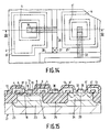
- Figures 14 and 15 show a semiconductor device 21 manufactured by means of the method described with reference to Figures 1 to 8.
- the starting material is a substrate region comprising a E -type substrate 22, an n-type buried layer 23 and a p-type epitaxial layer 24.
- regions insulated by oxide 25 are formed.
- a ptype base zone 16 is provided either by means of ion implantation or diffusion or by means of the processing steps as described, with reference to Figures 1 to 8.
- a masking layer 4 of oxide On the surface 3 again parts of a masking layer 4 of oxide are disposed, on which the layer 6,6' of polycrystalline silicon is formed, which is p-doped at the area of the base zone 16 (reference numeral 6 and is n-doped at other areas in this embodiment (reference numeral 6'). Diffusion from these polycrystalline silicon layers has formed the base contact zones 17 and the collector contact zones 20, respectively. At the area of the collector contact zone 20, beforehand a heavy doping with n-type impurities may have taken place. A part 35 of the layer 6' enclosed by oxide 13 remains in the opening 5' at the area of the collector metallization 32. This layer 6' is heavily doped, just like the part 14 at the area of the emitter zone 15, with n-type impurities at the last stage of the method. Otherwise, the reference numerals have the same meaning as in the preceding embodiments.
- the opening 5 is entirely enclosed at the area of the base zone 16 of p-type polycrystalline silicon 6.
- the base zone 16 can be connected with other elements by giving this layer 6 a defined pattern.
- a contact hole may be provided in the oxide 13 for contacting the layer 6 with, for example, an aluminium track.
- the opening 5' is entirely enclosed at the area of the collector contact zone 20 by an n-type polycrystalline silicon layer 6', which contacts the collector contact zone 20.
- two kinds of contacting are possible, i.e. via the polycrystalline silicon 6' and via the collector metallization 32. Such a double contacting may be advantageous in given circumstances.
- tracks 36 of polycrystalline silicon are disposed between the regions 6,6' of polycrystalline silicon. These tracks may be used for interconnection and may be provided, if required, with interruptions 37, as indicated, for example by etching or selective oxidation of parts of the tracks 36.
- Fig. 16 shows a plan view of a transistor in a process with diffused collector insulation manufactured by means of a method as described with reference to Figures 17 to 21, which show cross-sections of the device taken on the line XXI-XXI in Fig.16 at successive stages of the method.
- Fig. 17 substantially entirely corresponds to Fig. 5 on the understanding that the device 1 now comprises a p-type substrate region 2, in which an n-type collector zone 38 is formed via the opening 5 in the oxide layer 4 by means of diffusion or ion implantation.
- Thenitride 8 is patterned outside the opening 5, as indicated in Fig. 16.
- the anisotropic etching treatment reactive ion etching
- the layer 6 of polycrystalline silicon is also given such a pattern, the polycrystalline silicon remaining along two opposite edges of the opening 5, as indicated in Fig.16.
- Another possibility of obtaining such patterns of polycrystalline silicon not entirely surrounding the opening 5 consists in that the polycrystalline silicon 6 is oxidized selectively whilst using the patterned nitride 8 as an oxidation-preventing mask.
- the groove 11 is closed by oxidation, as a result of which oxide 13 is formed.
- the subsequent step after planarization with photolacquer, there is etched back until the nitride 8 located outside the opening 5 has been removed and the device is still protected by photolacquer within the opening, as shown diagrammatically by the broken line 12 in Fig. 18.
- the exposed polycrystalline silicon 6 then becomes p-type conducting by a boron diffusion.
- the device of Fig.18 is obtained.
- the exposed polycrystalline parts 6 and tracks are doped with phosphorus, after which the photomask 39 is removed again and the polycrystalline silicon is subjected to a heavy arsenic doping.
- the edges of polycrystalline silicon act as a diffusion source.
- an n +- emitter zone 15 is obtained in a p-type base zone 16.
- the phosphorus overdopes the boron and forms a collector contact zone 20.
- the device of Fig. 20 is obtained.
- the polycrystalline silicon 6 on the oxide 4 is oxidized on the upper side, after which the remaining nitride 8 is removed within the opening 5 so that via the remaining polycrystalline silicon 14 p-type impurities can be diffused into the semiconductor body for forming a base contact zone 17.
- a base contact metallization 31 has been provided photolithographically in a generally known manner
- the device of Fig. 21 is obtained with a transistor comprising a collector zone 3 8 and a collector contact zone 20 contacted via a poly-crystalline silicon track 6.
- the transistor further comprises an emitter zone 15, also contacted by a polycrystalline silicon track 6, and a base zone 16 which is connected through the base contact zone 17 and the polycrystalline silicon 14 to the contact metallization 31.
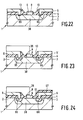
- the polycrystalline silicon layers 6 located on the edges are previously doped with boron, p-type regions 66 are formed during the step of closing the grooves 11 with oxide 13 due to the fact that the boron diffuses from the layers 6 into the semiconductor body 2.
- the photolacquer used for the planarization has been removed, in which step the polycrystalline layers 6 outside the depression 7 are exposed, these layers are provided, if required, by means of, for example, an arsenic implantation with n-type impurities, the nitride 8 and the oxide 13 acting as a mask.
- the device shown in Fig. 22 is obtained.
- a photolacquer mask 39 is provided (Fig. 23), by means of which the nitride 8 is partly etched away.
- an oxide layer 67 is applied, it is prevented that during etching of the polycrystalline silicon 6 exposed within the depression the remaining layers 6 are attacked. This may be effected, for example, by thermal oxidation, the doped polycrystalline silicon then oxidizing much more rapidly than the undoped polycrystalline silicon located within the depression, so that then the oxide grown within the depression on the polycrystalline layer 6 is removed again by means of a light etching treatment (Fig. 24). Before the oxidation step, the exposed layer 6 is doped with phosphorus.
- the exposed polycrystalline silicon 6 is then etched away down to the semiconductor surface 3, for example by means of plasma etching, the photolacquer layer 39 then being removed (Fig. 25).
- an oxide layer 67 is formed on it, whereupon also the groove 69 just mentioned is closed by oxidation (Fig. 26).
- the various kinds of impurities diffuse from the layers 6 into the semicondutor body and thus form the base zone 16, the emitter zone 15 and the collector contact zone 20.
- the poly- crystalline silicon 6 is doped with boron within the depression, which after diffusion into the semiconductor body 2 serves to form the base contact zone 17.
- the configuration of Fig. 27 is obtained, which after a metallization step substantially corresponds to that of Fig. 21 on the understanding that the base contact zone 17 is now located at a finite distance from the collector contact zone 20, which leads to a considerable reduction of the base-collector capacitance.
- Figures 28 to 35 show a method of manufacturing a lateral field effect transistor, in which the grooves 11 are formed by means of a slightly different method.
- the starting material is a device 41 having an n-type substrate region 2 and a masking layer 4 located on a surface 3 thereof.
- a p-type zone 42 is provided, for example by means of diffusion, whilst using the oxide 4 as a mask, the latter zone then being lightly oxidized to obtain a gate oxide 43.
- a layer 6 of polycrystalline silicon and a layer 8 of silicon nitride are again successively formed on the oxide 4 and within the opening 5 as well as a first convertible layer 9, in this case of polycrystalline silicon.
- the assembly is covered by a substantially uniform layer 44 of oxidation-preventing material, in this case silicon nitride, and a second convertible layer 45 of polycrystalline silicon.
- a substantially uniform layer 44 of oxidation-preventing material in this case silicon nitride
- a second convertible layer 45 of polycrystalline silicon is maintained in a manner similar to that in the preceding embodiments.
- the layer 45 is then selectively converted, which means in this case that an ion implantation with, for example, boron ions is carried out, as indicated diagrammatically by arrows 46.
- the layer 45 thus becomes E -type conducting,
- the parts 47 at the area of the depression 7 are again readily soluble in potassium hydroxide, while the remaining part of the layer 45 is substantially not attacked thereby and forms an auxiliary mask after the parts 47 have been dissolved.
- the auxiliary mask may also be formed by oxidizing the remaining parts of the layer 45 to an auxiliary mask 48 of silicon oxide. Whilst using this oxide 48 as a mask, the subjacent layer 44 of nitride is etched (see Fig. 29).
- the remaining nitride 44 forms an oxidation mask in the following processing step, in which the polycrystalline silicon 9 is converted along the inner edge of the depression 7 into oxide 49 (see Fig. 39),which is then removed by a wet-chemical treatment.
- the device of Fig. 31 is obtained, in which the layer 9 of polycrystalline silicon again constitutes an intermediate mask for etching the subjacent intride layer 8.
- the exposed parts of the nitride layer 8 and the nitride layer 44 are removed by wet-chemical etching.
- the device of Fig. 32 is obtained.
- a groove 11 is etched down to the gate oxide 43 by anisotropic etching.
- the groove 11 encloses a region 14 of poly- crystalline silicon.
- an n-type region 49 is formed in the p-type region 42 by ion implantation (see Fig. 33).
- the whole device is again coated with photolacquer, which is planarized and is then etched back until the nitride on the layer 6 outside the depression is removed.
- the groove 11 is closed by oxidation in a manner similar to that described with reference to Figures 1 to 6 so that the device of Fig. 34 is obtained with oxide 13 in the groove 11 and on the upper side of the polycrystalline silicon 6.
- the remaining nitride 8 and the polycrystalline silicon 14 are successively removed.
- the exposed oxide 43 is then removed so that this oxide remains only at the area of the polycrystalline silicon 6 and the thermal oxide 13.
- any oxide 43 damaged during the reactive ion etching is now situated below this oxide 13 and forms part of the insulation between the polycrystalline silicon layers 6 and a metallization 51 to be provided on the surface 2 (see Fig. 35).
- an implantation step is carried out with ions which cause the n-conductivity type in order to obtain a region 50, which together with the region 49 forms the source zone of a field effect transistor, whose gate region is constituted by the region 42 and whose gate electrode is constituted by the polycrystalline silicon 6, which is separated from the gate region 42 by the gate oxide 43.
- the n-type region 2 acts as the drain region and is connected through a highly doped n-type region 52 to a contact metallization 53.
- the field effect transistor 41 of Fig. 35 is obtained.
- This field effect transistor has a channel region of very short channel length (for example 0.5 / um) having a surface concentration of acceptor atoms substantially equal throughout the area below the gate oxide.
- Figures 36 to 38 show a modification of the part of the method as shown in Figures 1 to 5.
- the device 1 again comprises a semiconductor substrate 2 provided with a surface zone 16 and is provided at the major surface 3 with a first masking layer 4 of silicon oxide.
- a substantially uniform layer 6 of poly- crystalline silicon is formed on the substrate region 2 within the opening 5 in the layer 4-and on the adjoining oxide 4, but this layer is now covered at reduced pressure and at a temperature of 750 to 850 0 C with a substantially uniform layer 65 of silicon nitride and then with a substantially uniform layer of silicon oxide, from which a mask 10 is obtained in the same manner as described with reference to Fig. 3.
- the nitride layer 65 is now bombarded, for example, with arsenic; this implantation is carried out with an energy of 200 kV and a dose of 10 14 ions/cm 2 , after which the whole is subjected to a heat treatment of about 750 to 850°C for 15 to 20 minutes.
- the parts of the silicon nitride layer 65 irradiated by ions can be etched less satisfactorily than the parts protected by the mask 10, as described in the Netherlands Patent Application No. 8301262 (PHN.10638) filed on April 11 th 1983 by the Applicant.
- the parts of the layer 65 protected by the mask 10 are etched, after removal of this mask, in an aqueous solution containing about 4 % by volume of hydrofluoride.
- the layer 65 in this case plays the same part as the layers 8 and 9 in the embodiment of Figures 1 to 5.
- an anisotropic etching treatment can be carried out, which results in the device of Fig. 38, with which in the same manner shown in Figures 5 to 8 a semiconductor device can be manufactured.
- the nitride layer may of course also be bombarded with, for example, nitrogen, anitomony, boron, gallium, phosphorus, argon, krypton or xenon, as described more fully in the said Netherlands Patent Application No. 8301262.
- Such implantations are preferably carried out in a manner such that the ions penetrate as far as halfway the layer 65 of silicon nitride, the radiation doses being chosen between 10 12 and 10 15 ions/Cm 2 .
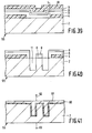
- the method according to the invention may also be used for devices other than semiconductor devices, such as, for example, a capacitor.
- the starting material is a substrate region 2 of tantalum, whose surface is covered by a mask 4 of tantalum oxide, which is obtained, for example, by oxidation of a surface layer of the tantalum or by anodization and then selective etching of this layer by means of reactive ion etching.
- the device 55 is then covered in the same manner as the device of Fig. 2 by a first convertible layer 6 of polycrystalline silicon, a second masking layer 8 of silicon nitride a second convertible layer 9 of polycrystalline silicon and a masking layer 10.
- grooves 11 are formed (see Fig. 40), the etching of the grooves being continued until they extend into the substrate region 2 of tantalum. After the remaining parts of the various layers have been removed from the surface, the substrate region 2, inclusive of the grooves 11, is covered by means of a light oxidation with a thin tantalum oxide layer 60 and a metal layer 61, for example of aluminium, is formed on the whole (Fig. 41). A capacitor with a dielectric 60 is then obtained between the connection terminals 62 and 63. The overall effective surface area of the capacitor is strongly increased due to the presence of the grooves so that on the same substrate surface a considerably larger capacitance can be realized than in the absence of the grooves.
- Such a capacitor may also be obtained by starting from a semiconductor substrate, in which beforehand depressions 57 are formed by selective reactive ion etching (see Fig. 42). The whole is covered by a convertible layer 6 of polycrystalline silicon and with a masking layer. After anisotropic etching of a masking layer 10 consisting of oxide, an oxide edge 10 remains in the depressions (Fig. 43). which protects the subjacent polycrystalline silicon 6 against conversion. After the conversion (doping with phosphorus or silicidation) the edge 10 and then the non ⁇ converted polycrystalline silicon 6 are removed; the remaining polycrystalline silicon 6 then again forms a mask for etching the grooves 11 (Fig. 44). The grooves and the surface are covered again with a dielectric 60, after which a second metal layer 61 is formed and the capacitor is provided with connection terminals 62 and 63. Thus, the device of Fig. 45 is obtained.
- the masking layer 4 may also be made of a double layer of nitride and oxide.
- the oxide 25 in Fig. 15 may be provided by local oxidation, but may also be provided by means of the method described in Figures 9 to 13.
- the conductivity types can be inverted (simultaneously).
Landscapes
- Engineering & Computer Science (AREA)
- Manufacturing & Machinery (AREA)
- Physics & Mathematics (AREA)
- Condensed Matter Physics & Semiconductors (AREA)
- General Physics & Mathematics (AREA)
- Computer Hardware Design (AREA)
- Microelectronics & Electronic Packaging (AREA)
- Power Engineering (AREA)
- Inorganic Chemistry (AREA)
- Chemical & Material Sciences (AREA)
- Bipolar Transistors (AREA)
- Element Separation (AREA)
- Drying Of Semiconductors (AREA)
Applications Claiming Priority (3)
| Application Number | Priority Date | Filing Date | Title |
|---|---|---|---|
| NL8402859A NL8402859A (nl) | 1984-09-18 | 1984-09-18 | Werkwijze voor het vervaardigen van submicrongroeven in bijvoorbeeld halfgeleidermateriaal en met deze werkwijze verkregen inrichtingen. |
| NL8402859 | 1984-09-18 | ||
| CN85103535A CN85103535B (zh) | 1984-09-18 | 1985-05-06 | 在材料(例如半导体材料)中加工亚微型槽的方法以及用这种方法制成的器件 |
Publications (3)
| Publication Number | Publication Date |
|---|---|
| EP0178000A2 true EP0178000A2 (de) | 1986-04-16 |
| EP0178000A3 EP0178000A3 (en) | 1986-04-23 |
| EP0178000B1 EP0178000B1 (de) | 1990-05-16 |
Family
ID=25741633
Family Applications (1)
| Application Number | Title | Priority Date | Filing Date |
|---|---|---|---|
| EP85201462A Expired EP0178000B1 (de) | 1984-09-18 | 1985-09-13 | Verfahren zur Herstellung submikronischer Gräben, z.B. in Halbleitermaterial und nach diesem Verfahren hergestellte Anordnungen |
Country Status (6)
| Country | Link |
|---|---|
| US (1) | US4717689A (de) |
| EP (1) | EP0178000B1 (de) |
| JP (1) | JPS6174342A (de) |
| CN (1) | CN85103535B (de) |
| DE (1) | DE3577776D1 (de) |
| NL (1) | NL8402859A (de) |
Cited By (4)
| Publication number | Priority date | Publication date | Assignee | Title |
|---|---|---|---|---|
| EP0288739A2 (de) * | 1987-04-30 | 1988-11-02 | International Business Machines Corporation | Selbstausrichtendes Verfahren einer Isolierungsgrubenstruktur zu einem implantierten Bereich |
| EP0290763A1 (de) * | 1987-05-11 | 1988-11-17 | International Business Machines Corporation | Hochleistungstransistor mit Seitenwandemitter |
| EP0313777A2 (de) * | 1987-10-30 | 1989-05-03 | International Business Machines Corporation | Verfahren zur Erhöhung der Konzentration der Dotierungsdichte für selektierte Zonen in Halbleiteranordnungen |
| US4916083A (en) * | 1987-05-11 | 1990-04-10 | International Business Machines Corporation | High performance sidewall emitter transistor |
Families Citing this family (13)
| Publication number | Priority date | Publication date | Assignee | Title |
|---|---|---|---|---|
| US4924287A (en) * | 1985-01-20 | 1990-05-08 | Avner Pdahtzur | Personalizable CMOS gate array device and technique |
| NL190388C (nl) * | 1986-02-07 | 1994-02-01 | Nippon Telegraph & Telephone | Werkwijze voor het vervaardigen van een halfgeleiderinrichting en halfgeleiderinrichting. |
| JPS63193562A (ja) * | 1987-02-06 | 1988-08-10 | Toshiba Corp | バイポ−ラトランジスタの製造方法 |
| IL82113A (en) * | 1987-04-05 | 1992-08-18 | Zvi Orbach | Fabrication of customized integrated circuits |
| US5008210A (en) * | 1989-02-07 | 1991-04-16 | Hewlett-Packard Company | Process of making a bipolar transistor with a trench-isolated emitter |
| JP2741964B2 (ja) * | 1991-04-15 | 1998-04-22 | シャープ株式会社 | 半導体装置の製造方法 |
| US5120668A (en) * | 1991-07-10 | 1992-06-09 | Ibm Corporation | Method of forming an inverse T-gate FET transistor |
| US5245206A (en) * | 1992-05-12 | 1993-09-14 | International Business Machines Corporation | Capacitors with roughened single crystal plates |
| US5414283A (en) * | 1993-11-19 | 1995-05-09 | Ois Optical Imaging Systems, Inc. | TFT with reduced parasitic capacitance |
| US5389559A (en) * | 1993-12-02 | 1995-02-14 | International Business Machines Corporation | Method of forming integrated interconnect for very high density DRAMs |
| KR0157928B1 (ko) * | 1995-12-27 | 1998-12-15 | 문정환 | 자체 접합형 아웃-리거 위상반전마스크 제조방법 |
| KR100456698B1 (ko) * | 2002-09-04 | 2004-11-10 | 삼성전자주식회사 | 강유전체 메모리 소자의 제조 방법 |
| JP5184476B2 (ja) * | 2009-09-17 | 2013-04-17 | 東京エレクトロン株式会社 | 基板液処理方法、基板液処理装置および記憶媒体 |
Citations (3)
| Publication number | Priority date | Publication date | Assignee | Title |
|---|---|---|---|---|
| GB2111304A (en) * | 1981-12-10 | 1983-06-29 | Philips Nv | Providing a groove in a substrate region |
| JPS58153373A (ja) * | 1982-03-08 | 1983-09-12 | Oki Electric Ind Co Ltd | 半導体素子の製造方法 |
| EP0098652A2 (de) * | 1982-07-05 | 1984-01-18 | Koninklijke Philips Electronics N.V. | Verfahren zur Herstellung eines Feldeffekttransistors mit einem isolierten Gate und nach diesem Verfahren hergestellte Anordnung |
Family Cites Families (11)
| Publication number | Priority date | Publication date | Assignee | Title |
|---|---|---|---|---|
| US3536547A (en) * | 1968-03-25 | 1970-10-27 | Bell Telephone Labor Inc | Plasma deposition of oxide coatings on silicon and electron bombardment of portions thereof to be etched selectively |
| US4053349A (en) * | 1976-02-02 | 1977-10-11 | Intel Corporation | Method for forming a narrow gap |
| JPS52128066A (en) * | 1976-04-20 | 1977-10-27 | Matsushita Electronics Corp | Manufacture of semiconductor device |
| CA1129118A (en) * | 1978-07-19 | 1982-08-03 | Tetsushi Sakai | Semiconductor devices and method of manufacturing the same |
| US4274909A (en) * | 1980-03-17 | 1981-06-23 | International Business Machines Corporation | Method for forming ultra fine deep dielectric isolation |
| JPS5864044A (ja) * | 1981-10-14 | 1983-04-16 | Toshiba Corp | 半導体装置の製造方法 |
| JPS5893343A (ja) * | 1981-11-30 | 1983-06-03 | Toshiba Corp | 半導体集積回路の分離領域形成方法 |
| JPS58175847A (ja) * | 1982-04-08 | 1983-10-15 | Toshiba Corp | 半導体装置の製造方法 |
| US4545114A (en) * | 1982-09-30 | 1985-10-08 | Fujitsu Limited | Method of producing semiconductor device |
| NL8301262A (nl) * | 1983-04-11 | 1984-11-01 | Philips Nv | Werkwijze voor het vervaardigen van een halfgeleiderinrichting, waarbij met behulp van ionenimplantatie patronen worden aangebracht in een laag siliciumnitride. |
| US4601778A (en) * | 1985-02-25 | 1986-07-22 | Motorola, Inc. | Maskless etching of polysilicon |
-
1984
- 1984-09-18 NL NL8402859A patent/NL8402859A/nl not_active Application Discontinuation
-
1985
- 1985-05-06 CN CN85103535A patent/CN85103535B/zh not_active Expired
- 1985-09-13 DE DE8585201462T patent/DE3577776D1/de not_active Expired - Lifetime
- 1985-09-13 EP EP85201462A patent/EP0178000B1/de not_active Expired
- 1985-09-16 US US06/776,330 patent/US4717689A/en not_active Expired - Fee Related
- 1985-09-18 JP JP60206181A patent/JPS6174342A/ja active Pending
Patent Citations (3)
| Publication number | Priority date | Publication date | Assignee | Title |
|---|---|---|---|---|
| GB2111304A (en) * | 1981-12-10 | 1983-06-29 | Philips Nv | Providing a groove in a substrate region |
| JPS58153373A (ja) * | 1982-03-08 | 1983-09-12 | Oki Electric Ind Co Ltd | 半導体素子の製造方法 |
| EP0098652A2 (de) * | 1982-07-05 | 1984-01-18 | Koninklijke Philips Electronics N.V. | Verfahren zur Herstellung eines Feldeffekttransistors mit einem isolierten Gate und nach diesem Verfahren hergestellte Anordnung |
Non-Patent Citations (5)
| Title |
|---|
| IBM TECHNICAL DISCLOSURE BULLETIN, vol. 21, no. 12, May 1979, pages 5035-5038, New York, US; E. BASSOUS et al.: "Method of fabricating high-performance igfet structures with highly controllable submicron effective channel lengths" * |
| IBM TECHNICAL DISCLOSURE BULLETIN, vol. 22, no. 8B, January 1980, pages 3688-3691, New York, US:; R.C. VARSHNEY: "Polysilicon oxide process for small line gaps" * |
| IBM TECHNICAL DISCLOSURE BULLETIN, vol. 26, no. 1, June 1983, pages 253-255, New York, US; S.G. BARBEE et al.: "Polysilicon base/emitter contact process" * |
| NEUES AUS DER TECHNIK, no. 1/2, 15th April 1983, pages 1,2, Vogel-Verlag, W}rzburg, DE; "Herstellung von Halbleiterbauelementen mit sehr geringen Abmessungen" * |
| PATENTS ABSTRACTS OF JAPAN, vol. 7, no. 272, 3rd December 1983, page 91 E 214; & JP - A - 58 153 373 (OKI DENKI KOGYO K.K.) 12-09-1983 * |
Cited By (7)
| Publication number | Priority date | Publication date | Assignee | Title |
|---|---|---|---|---|
| EP0288739A2 (de) * | 1987-04-30 | 1988-11-02 | International Business Machines Corporation | Selbstausrichtendes Verfahren einer Isolierungsgrubenstruktur zu einem implantierten Bereich |
| EP0288739A3 (de) * | 1987-04-30 | 1991-01-16 | International Business Machines Corporation | Selbstausrichtendes Verfahren einer Isolierungsgrubenstruktur zu einem implantierten Bereich |
| EP0290763A1 (de) * | 1987-05-11 | 1988-11-17 | International Business Machines Corporation | Hochleistungstransistor mit Seitenwandemitter |
| US4847670A (en) * | 1987-05-11 | 1989-07-11 | International Business Machines Corporation | High performance sidewall emitter transistor |
| US4916083A (en) * | 1987-05-11 | 1990-04-10 | International Business Machines Corporation | High performance sidewall emitter transistor |
| EP0313777A2 (de) * | 1987-10-30 | 1989-05-03 | International Business Machines Corporation | Verfahren zur Erhöhung der Konzentration der Dotierungsdichte für selektierte Zonen in Halbleiteranordnungen |
| EP0313777A3 (de) * | 1987-10-30 | 1991-10-23 | International Business Machines Corporation | Verfahren zur Erhöhung der Konzentration der Dotierungsdichte für selektierte Zonen in Halbleiteranordnungen |
Also Published As
| Publication number | Publication date |
|---|---|
| DE3577776D1 (de) | 1990-06-21 |
| CN85103535A (zh) | 1986-11-05 |
| CN85103535B (zh) | 1988-08-10 |
| EP0178000A3 (en) | 1986-04-23 |
| NL8402859A (nl) | 1986-04-16 |
| JPS6174342A (ja) | 1986-04-16 |
| EP0178000B1 (de) | 1990-05-16 |
| US4717689A (en) | 1988-01-05 |
Similar Documents
| Publication | Publication Date | Title |
|---|---|---|
| KR930001559B1 (ko) | 전계효과 트랜지스터 제조방법 | |
| US4488351A (en) | Method for manufacturing semiconductor device | |
| US4102733A (en) | Two and three mask process for IGFET fabrication | |
| EP0200372B1 (de) | Herstellung eines selbstausrichtenden Kontaktfensters in einer integrierten Schaltung | |
| EP0088922B1 (de) | Verfahren zum Herstellen von Elektroden und Verdrahtungsstreifen auf einer Halbleiteranordnung | |
| US5714393A (en) | Diode-connected semiconductor device and method of manufacture | |
| US4545114A (en) | Method of producing semiconductor device | |
| EP0076942B1 (de) | Verfahren zur Herstellung von integrierten Schaltungsanordnungen mit dielektrischen Isolationszonen | |
| EP0178000A2 (de) | Verfahren zur Herstellung submikronischer Gräben, z.B. in Halbleitermaterial und nach diesem Verfahren hergestellte Anordnungen | |
| EP0083785A2 (de) | Verfahren zur Herstellung von selbstalignierten Feldeffekttransistoren für integrierte Schaltungen | |
| US5204276A (en) | Method of manufacturing semiconductor device | |
| EP0201867B1 (de) | Verfahren zur Herstellung eines bipolaren Transistors | |
| US4822754A (en) | Fabrication of FETs with source and drain contacts aligned with the gate electrode | |
| KR100223832B1 (ko) | 반도체 소자 및 그 제조방법 | |
| US4689872A (en) | Method of manufacturing a semiconductor device | |
| JPS6249750B2 (de) | ||
| KR0175442B1 (ko) | 반도체장치 및 그 제조방법 | |
| US4523368A (en) | Semiconductor devices and manufacturing methods | |
| EP0311109A2 (de) | Verfahren zur Herstellung eines Feldeffekttransistors mit Übergangsgatter | |
| KR100209280B1 (ko) | 반도체 소자의 콘택홀 형성방법 | |
| KR100311103B1 (ko) | 반도체장치의제조방법 | |
| GB2070858A (en) | A shallow channel field effect transistor | |
| EP0409370A2 (de) | Bipolartransistor | |
| KR100274979B1 (ko) | 반도체소자내의콘택트형성방법 | |
| KR0140996B1 (ko) | 자기정렬된 저도핑된 접합형성방법 |
Legal Events
| Date | Code | Title | Description |
|---|---|---|---|
| PUAI | Public reference made under article 153(3) epc to a published international application that has entered the european phase |
Free format text: ORIGINAL CODE: 0009012 |
|
| PUAL | Search report despatched |
Free format text: ORIGINAL CODE: 0009013 |
|
| AK | Designated contracting states |
Kind code of ref document: A2 Designated state(s): DE FR GB IT NL |
|
| AK | Designated contracting states |
Kind code of ref document: A3 Designated state(s): DE FR GB IT NL |
|
| 17P | Request for examination filed |
Effective date: 19861015 |
|
| 17Q | First examination report despatched |
Effective date: 19880722 |
|
| GRAA | (expected) grant |
Free format text: ORIGINAL CODE: 0009210 |
|
| AK | Designated contracting states |
Kind code of ref document: B1 Designated state(s): DE FR GB IT NL |
|
| REF | Corresponds to: |
Ref document number: 3577776 Country of ref document: DE Date of ref document: 19900621 |
|
| ITF | It: translation for a ep patent filed |
Owner name: ING. C. GREGORJ S.P.A. |
|
| PGFP | Annual fee paid to national office [announced via postgrant information from national office to epo] |
Ref country code: GB Payment date: 19900831 Year of fee payment: 6 |
|
| ET | Fr: translation filed | ||
| PGFP | Annual fee paid to national office [announced via postgrant information from national office to epo] |
Ref country code: FR Payment date: 19900920 Year of fee payment: 6 |
|
| ITTA | It: last paid annual fee | ||
| PGFP | Annual fee paid to national office [announced via postgrant information from national office to epo] |
Ref country code: DE Payment date: 19901123 Year of fee payment: 6 |
|
| PLBE | No opposition filed within time limit |
Free format text: ORIGINAL CODE: 0009261 |
|
| STAA | Information on the status of an ep patent application or granted ep patent |
Free format text: STATUS: NO OPPOSITION FILED WITHIN TIME LIMIT |
|
| PG25 | Lapsed in a contracting state [announced via postgrant information from national office to epo] |
Ref country code: NL Effective date: 19910401 |
|
| 26N | No opposition filed | ||
| NLV4 | Nl: lapsed or anulled due to non-payment of the annual fee | ||
| PG25 | Lapsed in a contracting state [announced via postgrant information from national office to epo] |
Ref country code: GB Effective date: 19910913 |
|
| GBPC | Gb: european patent ceased through non-payment of renewal fee | ||
| PG25 | Lapsed in a contracting state [announced via postgrant information from national office to epo] |
Ref country code: FR Effective date: 19920529 |
|
| PG25 | Lapsed in a contracting state [announced via postgrant information from national office to epo] |
Ref country code: DE Effective date: 19920602 |
|
| REG | Reference to a national code |
Ref country code: FR Ref legal event code: ST |