EP0163384B1 - Power source lines arrangement in an integrated circuit - Google Patents
Power source lines arrangement in an integrated circuit Download PDFInfo
- Publication number
- EP0163384B1 EP0163384B1 EP85302251A EP85302251A EP0163384B1 EP 0163384 B1 EP0163384 B1 EP 0163384B1 EP 85302251 A EP85302251 A EP 85302251A EP 85302251 A EP85302251 A EP 85302251A EP 0163384 B1 EP0163384 B1 EP 0163384B1
- Authority
- EP
- European Patent Office
- Prior art keywords
- power source
- bus
- integrated circuit
- layer
- semiconductor integrated
- Prior art date
- Legal status (The legal status is an assumption and is not a legal conclusion. Google has not performed a legal analysis and makes no representation as to the accuracy of the status listed.)
- Expired
Links
Images


Classifications
-
- H10W20/496—
-
- H—ELECTRICITY
- H10—SEMICONDUCTOR DEVICES; ELECTRIC SOLID-STATE DEVICES NOT OTHERWISE PROVIDED FOR
- H10B—ELECTRONIC MEMORY DEVICES
- H10B12/00—Dynamic random access memory [DRAM] devices
-
- H—ELECTRICITY
- H10—SEMICONDUCTOR DEVICES; ELECTRIC SOLID-STATE DEVICES NOT OTHERWISE PROVIDED FOR
- H10D—INORGANIC ELECTRIC SEMICONDUCTOR DEVICES
- H10D88/00—Three-dimensional [3D] integrated devices
-
- H—ELECTRICITY
- H10—SEMICONDUCTOR DEVICES; ELECTRIC SOLID-STATE DEVICES NOT OTHERWISE PROVIDED FOR
- H10D—INORGANIC ELECTRIC SEMICONDUCTOR DEVICES
- H10D89/00—Aspects of integrated devices not covered by groups H10D84/00 - H10D88/00
- H10D89/211—Design considerations for internal polarisation
- H10D89/213—Design considerations for internal polarisation in field-effect devices
-
- H10W20/427—
Definitions
- said power regulated bus and said ground bus are disposed one over the other in a laminated manner along larger part of their length with a layer of a dielectric substance interposed therebetween so that said power regulated bus, said ground bus and said dielectric substance form a capacitance element.
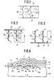
- a dielectric substance layer 30 made of, for instance, SiO 2 is further deposited over the connection layers 11 and 11', and a contact hole P 2 is provided through the layer 30 (the contact hole P 2 may otherwise be provided after the deposition of the insulating layer 70) at a position overlying N + diffusion layer 43 which is operable as a source electrode of the MOS FET pair 40 held in earth potential.
- an earth side connection layer 22 made of, for instance, aluminum and constituting the second layer is deposited entirely so that the layer 22 is electrically connected with the N + diffusion layer 43 through the hole P 2 .
- the earth side connection layer 22 is laminated in parallel with the power source side connection layer 11 with the dielectric substance layer 30 interposed therebetween. Furthermore, the opposing surfaces of the power source side connection layer 11 and the earth side connection layer 22 are positively increased so as to provide a required capacitance between the two layers.
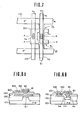
- the circuit shown in FIG. 5 is rearranged as shown in FIG. 6.
- the circuit shown in FIG. 6 is repeatedly arranged vertically along the lines 103, 104, 105, 106 and 107 into a required number of stages.
- the power source lines 80 and 90 in FIG. 5 are formed into a laminated construction. It is assumed that the power source line at the potential V DD is disposed in the first layer (the line in the first layer is designated by 81), while the power source line at the potential V ss is arranged in the second layer (the line in the second layer is designated by 92).
- a dielectric substance such as Si0 2 (CVD-Si0 2 ) is then formed over the entire surface, and the power source line 92 in the form of the second layer made of a metal such as AI and to be held at the power source voltage V ss is deposited on the dielectric substance layer 150 such that the power source line 92 extends in parallel with the power source line 81 provided in the form of the first layer.
- FIG. 9 is a time chart showing conditions of various signals during the sense operation of the dynamic RAM. According to the embodiment, it is possible to increase forcibly the power source potential V ss as shown by one-dot-dash line CL in FIG. 9 in synchronism with a precharging signal ⁇ ⁇ of the bit lines so that the electric charge in the capacitance between the power source lines 81 and 92 is effectively utilized for charging the bit lines. Such an operation can be realized by connecting the power source line 92 at a potential V ss with a suitable power source not shown for increasing the potential of the power source line 92 for a time synchronized with the precharging signal ⁇ ⁇ .
- the capacitance C is calculated as follows. This indicates that a stable operation of the integrated circuit can be assured for a capacitance C more than 0.25 nF.
- the condition related to the limiting value AV of the voltage drop is varied depending on the size and the kind of the semiconductor integrated circuit.
- the limiting value AV of approximately 50% of the power source voltage is utilized for determining the required value of the capacitance C, and in case where the condition becomes more strict, a limiting value AV of 20% or 10% of the power source voltage is selected thereby determining the capacitance C.
Landscapes
- Internal Circuitry In Semiconductor Integrated Circuit Devices (AREA)
- Semiconductor Integrated Circuits (AREA)
- Semiconductor Memories (AREA)
Applications Claiming Priority (2)
| Application Number | Priority Date | Filing Date | Title |
|---|---|---|---|
| JP59062926A JPS60206161A (ja) | 1984-03-30 | 1984-03-30 | 半導体集積回路 |
| JP62926/84 | 1984-03-30 |
Publications (2)
| Publication Number | Publication Date |
|---|---|
| EP0163384A1 EP0163384A1 (en) | 1985-12-04 |
| EP0163384B1 true EP0163384B1 (en) | 1990-03-21 |
Family
ID=13214367
Family Applications (1)
| Application Number | Title | Priority Date | Filing Date |
|---|---|---|---|
| EP85302251A Expired EP0163384B1 (en) | 1984-03-30 | 1985-04-01 | Power source lines arrangement in an integrated circuit |
Country Status (3)
| Country | Link |
|---|---|
| EP (1) | EP0163384B1 (enExample) |
| JP (1) | JPS60206161A (enExample) |
| DE (1) | DE3576763D1 (enExample) |
Families Citing this family (16)
| Publication number | Priority date | Publication date | Assignee | Title |
|---|---|---|---|---|
| JPS639137U (enExample) * | 1986-07-03 | 1988-01-21 | ||
| JPS63158851A (ja) * | 1986-12-22 | 1988-07-01 | Nec Corp | 半導体集積回路装置 |
| JPS63164352A (ja) * | 1986-12-26 | 1988-07-07 | Nec Corp | 半導体集積回路 |
| JP2606845B2 (ja) * | 1987-06-19 | 1997-05-07 | 富士通株式会社 | 半導体集積回路 |
| JPH0654774B2 (ja) * | 1987-11-30 | 1994-07-20 | 株式会社東芝 | 半導体装置及びその製造方法 |
| JPH01283863A (ja) * | 1988-05-10 | 1989-11-15 | Nec Corp | Mos型半導体装置 |
| JPH01297839A (ja) * | 1988-05-26 | 1989-11-30 | Toshiba Corp | 半導体装置 |
| JPH0750708B2 (ja) * | 1989-04-26 | 1995-05-31 | 株式会社東芝 | 半導体装置 |
| JPH0430388A (ja) * | 1990-05-25 | 1992-02-03 | Oki Electric Ind Co Ltd | 半導体記憶回路 |
| US5280453A (en) * | 1990-05-31 | 1994-01-18 | Oki Electric Industry Co., Ltd. | Semiconductor memory device with noise reduction system |
| JP3031966B2 (ja) * | 1990-07-02 | 2000-04-10 | 株式会社東芝 | 集積回路装置 |
| JPH06140607A (ja) * | 1992-10-28 | 1994-05-20 | Mitsubishi Electric Corp | 半導体集積回路 |
| FR2713399B1 (fr) * | 1993-12-01 | 1996-03-01 | Matra Mhs | Dispositif de réduction du niveau de bruit d'un circuit intégré à plusieurs niveaux de conducteurs. |
| JPH07169807A (ja) * | 1993-12-16 | 1995-07-04 | Nippondenso Co Ltd | 半導体ウェハ |
| KR20010040904A (ko) | 1998-12-16 | 2001-05-15 | 인피니언 테크놀로지스 아게 | 용량성 성분들을 가지는 집적 회로 |
| JP2001118988A (ja) | 1999-10-15 | 2001-04-27 | Mitsubishi Electric Corp | 半導体装置 |
Family Cites Families (5)
| Publication number | Priority date | Publication date | Assignee | Title |
|---|---|---|---|---|
| US4261772A (en) * | 1979-07-06 | 1981-04-14 | American Microsystems, Inc. | Method for forming voltage-invariant capacitors for MOS type integrated circuit device utilizing oxidation and reflow techniques |
| US4471374A (en) * | 1980-06-30 | 1984-09-11 | Inmos Corporation | Single polycrystalline silicon memory cell |
| FR2493045A1 (fr) * | 1980-10-23 | 1982-04-30 | Thomson Csf | Structure de capacite dans un circuit integre a deux niveaux de metallisation et procede de fabrication |
| JPS5780828A (en) * | 1980-11-07 | 1982-05-20 | Hitachi Ltd | Semiconductor integrated circuit device |
| JPS594050A (ja) * | 1982-06-30 | 1984-01-10 | Fujitsu Ltd | 半導体装置 |
-
1984
- 1984-03-30 JP JP59062926A patent/JPS60206161A/ja active Granted
-
1985
- 1985-04-01 EP EP85302251A patent/EP0163384B1/en not_active Expired
- 1985-04-01 DE DE8585302251T patent/DE3576763D1/de not_active Expired - Lifetime
Also Published As
| Publication number | Publication date |
|---|---|
| JPH0552671B2 (enExample) | 1993-08-06 |
| DE3576763D1 (de) | 1990-04-26 |
| JPS60206161A (ja) | 1985-10-17 |
| EP0163384A1 (en) | 1985-12-04 |
Similar Documents
| Publication | Publication Date | Title |
|---|---|---|
| EP0163384B1 (en) | Power source lines arrangement in an integrated circuit | |
| EP0202515B1 (en) | Semiconductor memory | |
| EP0046011B1 (en) | Semiconductor memory device | |
| KR100218622B1 (ko) | 면적효율이 우수한 용량소자를 갖는 반도체장치 | |
| KR900000170B1 (ko) | 다이내믹형 메모리셀과 그 제조방법 | |
| JPH0476215B2 (enExample) | ||
| JPS61280651A (ja) | 半導体記憶装置 | |
| EP0112670A1 (en) | Semiconductor memory device having stacked capacitor-tape memory cells | |
| US4809046A (en) | Semiconductor memory device | |
| JPS6316658A (ja) | 半導体記憶装置 | |
| US6078074A (en) | Semiconductor device having multilayer metal interconnection | |
| JP2584986B2 (ja) | 半導体装置の配線構造 | |
| US7498207B2 (en) | Semiconductor memory device and manufacturing method of the same | |
| EP0046629B1 (en) | Semi-conductor memory device having an insulated gate field effect transistor as a fundamental element | |
| US5202751A (en) | Semiconductor integrated circuit | |
| KR100293079B1 (ko) | 반도체장치 | |
| KR950008671B1 (ko) | 비트라인 사이에 감소된 기생용량을 갖는 반도체 기억장치 | |
| JPS6173367A (ja) | 半導体装置 | |
| US4839710A (en) | CMOS cell which can be used as a resistor, a capacitor, an RC component or a terminating impedance of a signal | |
| US4482825A (en) | Semiconductor device having a circuit for generating a voltage higher than a supply voltage and responsive to variations in the supply voltage | |
| JPS60250665A (ja) | 半導体記憶装置 | |
| JPH0691216B2 (ja) | 半導体記憶装置 | |
| KR0144944B1 (ko) | 스태틱 랜덤 억세스 메모리 소자 | |
| JPH0321104B2 (enExample) | ||
| JPS60121763A (ja) | 半導体メモリ装置 |
Legal Events
| Date | Code | Title | Description |
|---|---|---|---|
| PUAI | Public reference made under article 153(3) epc to a published international application that has entered the european phase |
Free format text: ORIGINAL CODE: 0009012 |
|
| AK | Designated contracting states |
Designated state(s): DE FR GB NL |
|
| 17P | Request for examination filed |
Effective date: 19860603 |
|
| 17Q | First examination report despatched |
Effective date: 19871029 |
|
| GRAA | (expected) grant |
Free format text: ORIGINAL CODE: 0009210 |
|
| AK | Designated contracting states |
Kind code of ref document: B1 Designated state(s): DE FR GB NL |
|
| REF | Corresponds to: |
Ref document number: 3576763 Country of ref document: DE Date of ref document: 19900426 |
|
| ET | Fr: translation filed | ||
| PLBE | No opposition filed within time limit |
Free format text: ORIGINAL CODE: 0009261 |
|
| STAA | Information on the status of an ep patent application or granted ep patent |
Free format text: STATUS: NO OPPOSITION FILED WITHIN TIME LIMIT |
|
| 26N | No opposition filed | ||
| PGFP | Annual fee paid to national office [announced via postgrant information from national office to epo] |
Ref country code: GB Payment date: 19970324 Year of fee payment: 13 |
|
| PGFP | Annual fee paid to national office [announced via postgrant information from national office to epo] |
Ref country code: DE Payment date: 19970404 Year of fee payment: 13 |
|
| PGFP | Annual fee paid to national office [announced via postgrant information from national office to epo] |
Ref country code: FR Payment date: 19970409 Year of fee payment: 13 |
|
| PG25 | Lapsed in a contracting state [announced via postgrant information from national office to epo] |
Ref country code: GB Free format text: LAPSE BECAUSE OF NON-PAYMENT OF DUE FEES Effective date: 19980401 |
|
| PG25 | Lapsed in a contracting state [announced via postgrant information from national office to epo] |
Ref country code: FR Free format text: THE PATENT HAS BEEN ANNULLED BY A DECISION OF A NATIONAL AUTHORITY Effective date: 19980430 |
|
| GBPC | Gb: european patent ceased through non-payment of renewal fee |
Effective date: 19980401 |
|
| PG25 | Lapsed in a contracting state [announced via postgrant information from national office to epo] |
Ref country code: DE Free format text: LAPSE BECAUSE OF NON-PAYMENT OF DUE FEES Effective date: 19990202 |
|
| REG | Reference to a national code |
Ref country code: FR Ref legal event code: ST |
|
| PGFP | Annual fee paid to national office [announced via postgrant information from national office to epo] |
Ref country code: NL Payment date: 20040406 Year of fee payment: 20 |
|
| PG25 | Lapsed in a contracting state [announced via postgrant information from national office to epo] |
Ref country code: NL Free format text: LAPSE BECAUSE OF EXPIRATION OF PROTECTION Effective date: 20050401 |
|
| NLV7 | Nl: ceased due to reaching the maximum lifetime of a patent |
Effective date: 20050401 |