EP0143624A2 - Dynamische Halbleiterspeicheranordnung mit geteilten Speicherzellenblöcken - Google Patents
Dynamische Halbleiterspeicheranordnung mit geteilten Speicherzellenblöcken Download PDFInfo
- Publication number
- EP0143624A2 EP0143624A2 EP84308140A EP84308140A EP0143624A2 EP 0143624 A2 EP0143624 A2 EP 0143624A2 EP 84308140 A EP84308140 A EP 84308140A EP 84308140 A EP84308140 A EP 84308140A EP 0143624 A2 EP0143624 A2 EP 0143624A2
- Authority
- EP
- European Patent Office
- Prior art keywords
- transfer gate
- data
- output
- test
- gate means
- Prior art date
- Legal status (The legal status is an assumption and is not a legal conclusion. Google has not performed a legal analysis and makes no representation as to the accuracy of the status listed.)
- Granted
Links
Images


Classifications
-
- G—PHYSICS
- G11—INFORMATION STORAGE
- G11C—STATIC STORES
- G11C29/00—Checking stores for correct operation ; Subsequent repair; Testing stores during standby or offline operation
-
- G—PHYSICS
- G06—COMPUTING OR CALCULATING; COUNTING
- G06F—ELECTRIC DIGITAL DATA PROCESSING
- G06F11/00—Error detection; Error correction; Monitoring
- G06F11/07—Responding to the occurrence of a fault, e.g. fault tolerance
- G06F11/16—Error detection or correction of the data by redundancy in hardware
- G06F11/1666—Error detection or correction of the data by redundancy in hardware where the redundant component is memory or memory area
- G06F11/167—Error detection by comparing the memory output
-
- G—PHYSICS
- G11—INFORMATION STORAGE
- G11C—STATIC STORES
- G11C11/00—Digital stores characterised by the use of particular electric or magnetic storage elements; Storage elements therefor
- G11C11/21—Digital stores characterised by the use of particular electric or magnetic storage elements; Storage elements therefor using electric elements
- G11C11/34—Digital stores characterised by the use of particular electric or magnetic storage elements; Storage elements therefor using electric elements using semiconductor devices
- G11C11/40—Digital stores characterised by the use of particular electric or magnetic storage elements; Storage elements therefor using electric elements using semiconductor devices using transistors
- G11C11/401—Digital stores characterised by the use of particular electric or magnetic storage elements; Storage elements therefor using electric elements using semiconductor devices using transistors forming cells needing refreshing or charge regeneration, i.e. dynamic cells
- G11C11/4063—Auxiliary circuits, e.g. for addressing, decoding, driving, writing, sensing or timing
- G11C11/407—Auxiliary circuits, e.g. for addressing, decoding, driving, writing, sensing or timing for memory cells of the field-effect type
- G11C11/409—Read-write [R-W] circuits
- G11C11/4096—Input/output [I/O] data management or control circuits, e.g. reading or writing circuits, I/O drivers or bit-line switches
-
- G—PHYSICS
- G11—INFORMATION STORAGE
- G11C—STATIC STORES
- G11C19/00—Digital stores in which the information is moved stepwise, e.g. shift registers
-
- G—PHYSICS
- G11—INFORMATION STORAGE
- G11C—STATIC STORES
- G11C29/00—Checking stores for correct operation ; Subsequent repair; Testing stores during standby or offline operation
- G11C29/04—Detection or location of defective memory elements, e.g. cell constructio details, timing of test signals
- G11C29/08—Functional testing, e.g. testing during refresh, power-on self testing [POST] or distributed testing
- G11C29/12—Built-in arrangements for testing, e.g. built-in self testing [BIST] or interconnection details
- G11C29/18—Address generation devices; Devices for accessing memories, e.g. details of addressing circuits
- G11C29/26—Accessing multiple arrays
-
- G—PHYSICS
- G11—INFORMATION STORAGE
- G11C—STATIC STORES
- G11C29/00—Checking stores for correct operation ; Subsequent repair; Testing stores during standby or offline operation
- G11C29/70—Masking faults in memories by using spares or by reconfiguring
Definitions
- the present invention relates to a semiconductor memory device having memory cells divided into a plurality of separated blocks, and more particularly, to a semiconductor memory device having a test circuit enabling a simultaneous test for the plurality of blocks.
- MOS random access memories have been enlarged to 1 Mbit.
- MOS metal-oxide semiconductor.
- test time period for such devices also increased.
- the test time period thereof is remarkably increased.
- the number of memory cells connected to one sense amplifier for the read operation has become higher and, accordingly, the load of each sense amplifier has also become higher so as to reduce the speed of the read operation.
- two or more series of sense amplifiers are provided. That is, the memory cells, sense amplifiers, row address decoders, and the like are divided into two or more blocks. However, such division can increase the time needed to test the memory device.
- An embodiment of the present invention can provide a semiconductor memory device having memory cells divided into a plurality of blocks, a means for writing data in parallel into the plurality of blocks and a means for comparing data read out of the plurality of blocks.
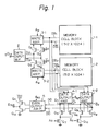
- Fig. 1 which illustrates a prior art dynamic RAM
- 1 Mbit memory cells are divided into two 512 kbit memory cell blocks 1-1 and 1-2.
- a data input buffer 2 receives an input data signal T D in of a transistor-transistor logic (TTL) level, and, as a result, generates an input data signal D in of a metal-oxide semiconductor (MOS) level and its inverted signal.
- TTL transistor-transistor logic
- MOS metal-oxide semiconductor
- the input data signals D in and D in are supplied via the transistors Q 1 and Q 2 to the write amplifiers 3-1, and in addition, are supplied via the transistors Q 3 and Q 4 to the write amplifier 3-2.
- the transistors Q 1 and Q 2 are controlled by one bit of row address signals such as an upper bit A 0
- the transistors Q 3 and Q 4 are controlled by its inverted signal A 0 .
- the data signals D in and D in are transmitted via the transistors Q l and Q 2 to the write amplifier 3-1.
- One memory cell is then selected within the memory cell block 1-1 by the row and column address decoders, not shown, and a write operation of data from the write amplifier 3-1 is performed upon the selected memory cell by using data buses DB 1 and DB 1 . Contrary to this, when the potential of address signal A 0 is low, and accordingly, the potential of the address signal A 0 is high, the data signals D in and D in are transmitted via the transistors Q 3 and Q 4 to the write amplifier 3-2. One memory cell is then selected within the memory cell block 1-2 by the row and column address decoders, not shown, and a write operation of data from the write amplifier 3-2 is performed upon the selected memory cell by using data buses DB 2 and DB 2 .
- a write operation is performed upon only one block, i.e., one of the memory cell blocks 1-1 and 1-2.
- two data output amplifiers 4-1 and 4-2 clccked by a clock signal ⁇ R1 , transistors Q 5 through Q12 , and a data output buffer 5 clocked by a clock signal ⁇ R2 are provided.
- the transistors Q 5 , Q 6 , and Q7 serve as a selection circuit for selectively connecting the outputs D 1 and D 1 of the data output amplifier 4-1 to data output buses DO and DO
- the transistors Q 8 , Q 9 , and Q 10 serve as-a selection circuit for selectively connecting the outputs D 2 and D 2 of the data output amplifier 4-2 to the data output buses DO and DO.
- the potentials of the data output buses DO and DO are transmitted via the data output buffer 5 to the transistors Q 11 and Q 12 which serve as a data output buffer.
- the transistor Q 7 is controlled by the address signal A 0
- the transistor Q 10 is controlled by the address signal A 0 . Therefore, only one of the data output amplifiers 4-1 and 4-2 is selectively connected to the data output buses DO and DO.
- the address signal A 0 is high
- the transistor Q 7 is turned on, so that one of the transistors Q 5 and Q 6 is turned on and the other is turned off.
- the outputs D 1 and D 1 are transmitted via the transistors Q 5 and Q 6 to the data output buses DO and DO .
- the transistor Q 10 is turned on, so that one of the transistors Q 8 and Q 9 is turned on and the other is turned off.
- the outputs D 2 and D 2 are transmitted via the transistors Q 8 and Q 9 to the data output buses DO and DO.
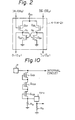
- each of the data output amplifiers 4-1 and 4-2 is fully illustrated in Fig. 2. That is, each of the data output amplifiers 4-1 and 4-2 comprises two transistors Q 21 and Q 22 clocked by the clock signal ⁇ R1 and controlled by the potentials at the data buses DB 1 and DB 1 (or DB 2 and DB 2 ), and further comprises two cross-coupled transistors Q 23 and Q 24 which form a flip-flop.
- the potentials at nodes N 1 and N 2 are transmitted as the outputs D1 and D 1 (or D 2 and D 2 ) to the gates of the transistors Q 5 and Q 6 (or Q 8 and Q 9 ).
- the data output buffer 5 has the same configuration as the circuit of Fig. 2.
- a test pad TP1 a pulling-down resistor R 3 , and transistors Q 31 , Q 32 , Q 33 , and Q 34 are added to the elements of the device of Fig. 1, thereby performing a write operation of the same input data D in upon both of the blocks, i.e., both of the memory cell blocks 1-1 and 1-2, simultaneously. That is, the elements TP1, R 3 ' Q 31 ' Q 32 ' Q 33 , and Q 34 form a simultaneous write enable circuit for the memory cell blocks 1-1 and 1-2.
- transistors Q 35 , Q 36 , Q 37 ' and Q38 , pulling - u p resistors R 4 and R 5 , and test pads TP2 and TP3 are added to the elements of the device of Fig. 1, thereby comparing the outputs D 1 and D 1 of the data output amplifier 4-1 with the outputs D 2 and D 2 of the data output amplifier 4-2. That is, the elements Q 35 ' Q 36 ' Q 37 ' Q 38 , R 4 ' R 5 , TP2, and TP3 form a comparison circuit for the outputs of the memory cell blocks 1-1 and 1-2.
- the device of Fig. 3 operates in the same way as the device of Fig. 1.
- the output comparison circuit formed by the elements Q 35 , Q 36 , Q 37 , Q 38 , R 4 , R 5 , TP2, and TP3 does not affect the normal operation.
- a high potential is applied to the test pad TP1, so that the transistors Q 31 , Q 32 , Q 33 , and Q 34 are turned on.
- the input data D in is supplied to the write amplifiers 3-1 and 3-2, and accordingly, the input data D in is written into one memory cell of each memory cell block 1-1 and 1-2.
- the selection of this one memory cell is carried out by the row and column address decoders (not shown).
- the pulling-up resistor R 3 linked between the test pad TP1 and the ground is provided for pulling down the potential at the test pad TP1 to a low level when the test pad 1 is in an open state.
- the transistors Q 35 and Q 37 are turned on and the transistors Q 36 and Q 38 are cut off.
- the potentials at the test pads TP2 and TP3 are at a low level and at a high level, respectively.
- the transistors Q 36 and Q 38 are turned on and the transistors Q 35 and Q 37 are cut off.
- the potentials at the test pads TP2 and TP3 are at a high level and at a low level, respectively.
- the potentials at the test pads TP2 and TP3 are both at a low level, as shown in Fig. 4.
- the transistors Q 35 , and Q 38 are both turned on and the transistors Q 36 and Q 37 are cut off, and accordingly, the potentials at the test pads TP2 and TP3 are both at a low level.
- the state wherein the potentials at the test pads TP2 and TP3 are both low exhibits an error state; i.e., one of the memory cell blocks 1-1 and 1-2 is erroneously operated.
- Fig. 5 which is a modification of the simultaneous write enable circuit of Fig. 3, the gate potentials of the transistors Q 1 , Q 2 , Q 3 , and Q 4 are controlled, thereby switching the normal operation mode and the test operation mode.
- a depletion-type transistor Q 51 , enhancement-type transistors Q 52 and Q 53 , a depletion-type transistor Q 54 , enhancement-type transistors Q 55 and Q 56 , and a test pad TP1' are provided.
- the transistors Q 51 , Q 52 , and Q 53 form a NAND circuit
- the transistors Q 54 , Q 55 , Q 56 also form a NAND circuit.
- the potential at the test pad TPl' is high, so that the NAND circuit formed by the transistors Q 51 , Q 52 , and Q 53 serves as an inverter for the address signal A 0 , and the NAND circuit formed by the transistors Q 54 , Q 55 , and Q 56 also serves as an inverter for the address signal A 0 . Therefore, the circuit of Fig. 5 operates in the same way as the device of Fig. 1.
- the test pad TP1' is in an open state, so that the charge of the test pad TP1' is discharged via the resistor R 3 , thereby decreasing the potential at the test pad TP1'.
- the transistors Q 52 and Q 55 are both cut off, and the gate potentials of the transistors Q 1 , Q2 ' Q 3 , and Q 4 remain high, by the depletion-type transistors Q 51 and Q 54 .
- the input data D in is supplied to the write amplifiers 3-1 and 3-2, and accordingly, the input data D in is written into one memory cell of each memory cell block 1-1 and 1-2.
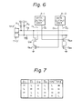
- Fig. 6 which is modification of the output comparison circuit of Fig. 3, transistors-Q 61 and Q 62 are provided in series, and transistors Q 63 and Q 64 are also provided in series.
- the operation of the circuit of Fig. 6 is shown in a truth table of Fig. 7. This table shows that the state wherein the potentials at the test pads TP2' and TP3' are both high exhibits an error state; i.e., one of the memory cell blocks 1-1 and 1-2 is erroneously operated. Note that, if there are more than three data output amplifiers, i.e., more than three memory cell blocks, it is possible to carry out an output comparison thereupon by increasing the number of transistors connected in series.
- transistors Q 81 through Q 90 are provided for fcur data output amplifiers 4-1 through 4-4.
- the transistors Q81 through Q 84 correspond to the transistor Q 35 through Q 38 of Fi g. 3, respectively, and the transistors Q 86 through Q 89 also correspond to the transistors Q 35 through Q 38 of Fig. 3, respectively.
- a common test is required for all the data output amplifiers 4-1 through 4-4, a high potential is applied to both of the test pads TP4 and TP5. Contrary to this, when a partial test is required for the data output amplifiers 4-1 and 4-2, a high potential is applied to only the test pad TP4.
- Fig. 9 which is still another modification of the output comparison circuit of Fig. 3, the data output buses DO and DO also serve as test buses TB and TB , and accordingly, the test pads TP2 and TP3 (or TP2' and TP3') are not provided. Therefore, the result of the output comparison circuit is obtained at the output of the output buffer formed by the transistors Q 11 and Q 12 of Fig. 3.
- transistors Q 7 ' and Q 10 ' which correspond to the transistors Q 7 and Q 10 , respectively, are provided.
- the gate potentials of the transistors Q 7 ' and Q 10 ' are controlled by a circuit formed by transistors Q 91 through Q 98 and the test pad TP1 and the pulling-down resistor R 3 .
- the transistors Q 91 and Q 92 serve as an inverter.
- the transistors Q 93 , Q 94 , and Q 95 form a NAND circuit
- the transistors Q 96 , Q 97 , Q 98 also form a NAND circuit.
- the test pad TP1 and the pulling-down resistor R 3 are the same as those of Fig. 3.
- the test pad TP1 is in an open state, so that the charge of the test pad TPl is discharged via the resistor R 3 thereby decreasing the potential at the test pad TP1.
- the inverter formed by the transistors Q 91 and Q 92 generates a high potential. Therefore, the NAND circuit formed by the transistors Q 93 , Q 94 , and Q95 serves as an inverter for the address signal A 0 , and the NAND circuit formed by the transistors Q 96 , Q 97 , and Q 98 also serves as an inverter for the address signal A 0 . Therefore, the circuit of Fig. 9 operates in the same way as the device of Fig. 1.
- the data output buses DO and DO serve as the test buses TB and TB of Fig. 3. That is, the state wherein the potentials at the data output buses DO and DO are both low exhibits an error state; i.e., one of the memory cell blocks 1-1 and 1-2 (Fig. 3) is erroneously operated. Note that when the potentials at the data output buses DO and DO are both low, the output D out of the data output buffer formed by the transistors Q 11 and Q 12 reaches a high impedance state.
- Fig. 10 which is an additional circuit for a test pad such as TP1
- the test pad TP1 is connected via depletion-type transistors Q 101 ' Q 102 , and Q 103 , and a resistor R 8 to a pad P for a normal operation.
- a pad P is connected to a lead pin by wire bonding or the like in assembling processes.
- the above-mentioned test pads are usually provided inside of the memory device, and accordingly, the test pads are sealed after the completion of the memory device. Therefore, if it is required to test the memory device even after the completion thereof, it is possible to do so by connecting the test pads via inverters or the like to the pads for use in a normal operation.
- a test for a large capacity memory device can be carried out in a very short time period.
- an embodiment of the present invention may advantageously provide a dynamic semiconductor memory device comprising a plurality of blocks of memory cells, said blocks being separated from each other; a plurality of write means, each provided for one of said memory cell blocks, for writing data thereinto; a simultaneous write enable circuit, connected to said write means, for simultaneously performing a write operation via said plurality of write means upon said plurality of memory cell blocks; a plurality of data output means, each provided for one of said memory cell blocks, for storing data read out of said memory cell blocks, each of said data output means having true and complementary output signal lines; a pair of output means, one of said output means being driven by the true signal lines of said data output means, the other being driven by the complementary signal lines of said data output means; and a means, connected to said pair of output means, for transmitting the logic level of said pair of output means to the exterior.
Landscapes
- Engineering & Computer Science (AREA)
- Microelectronics & Electronic Packaging (AREA)
- Computer Hardware Design (AREA)
- Theoretical Computer Science (AREA)
- General Physics & Mathematics (AREA)
- General Engineering & Computer Science (AREA)
- Physics & Mathematics (AREA)
- Quality & Reliability (AREA)
- Databases & Information Systems (AREA)
- For Increasing The Reliability Of Semiconductor Memories (AREA)
- Dram (AREA)
- Techniques For Improving Reliability Of Storages (AREA)
- Debugging And Monitoring (AREA)
Applications Claiming Priority (2)
| Application Number | Priority Date | Filing Date | Title |
|---|---|---|---|
| JP220553/83 | 1983-11-25 | ||
| JP58220553A JPS60115099A (ja) | 1983-11-25 | 1983-11-25 | 半導体記憶装置 |
Publications (3)
| Publication Number | Publication Date |
|---|---|
| EP0143624A2 true EP0143624A2 (de) | 1985-06-05 |
| EP0143624A3 EP0143624A3 (en) | 1987-10-14 |
| EP0143624B1 EP0143624B1 (de) | 1990-09-05 |
Family
ID=16752792
Family Applications (1)
| Application Number | Title | Priority Date | Filing Date |
|---|---|---|---|
| EP84308140A Expired EP0143624B1 (de) | 1983-11-25 | 1984-11-23 | Dynamische Halbleiterspeicheranordnung mit geteilten Speicherzellenblöcken |
Country Status (5)
| Country | Link |
|---|---|
| US (1) | US4744061A (de) |
| EP (1) | EP0143624B1 (de) |
| JP (1) | JPS60115099A (de) |
| KR (1) | KR900006159B1 (de) |
| DE (1) | DE3483134D1 (de) |
Cited By (14)
| Publication number | Priority date | Publication date | Assignee | Title |
|---|---|---|---|---|
| EP0186040A1 (de) * | 1984-12-28 | 1986-07-02 | Siemens Aktiengesellschaft | Integrierter Halbleiterspeicher |
| EP0197363A1 (de) * | 1985-03-26 | 1986-10-15 | Siemens Aktiengesellschaft | Verfahren zum Betreiben eines Halbleiterspeichers mit integrierter Paralleltestmöglichkeit und Auswerteschaltung zur Durchführung des Verfahrens |
| DE3639169A1 (de) * | 1986-01-21 | 1987-07-23 | Mitsubishi Electric Corp | Halbleiterspeichervorrichtung |
| EP0283907A1 (de) * | 1987-03-16 | 1988-09-28 | Siemens Aktiengesellschaft | Schaltungsanordnung und Verfahren zum Testen von Speicherzellen |
| EP0286852A1 (de) * | 1987-03-16 | 1988-10-19 | Siemens Aktiengesellschaft | Schaltungsanordnung und Verfahren zum Testen von Speicherzellen |
| EP0193210A3 (de) * | 1985-02-28 | 1988-12-14 | Nec Corporation | Halbleiterspeichergerät mit einer eingebauten Prüfschaltung |
| EP0267587A3 (de) * | 1986-11-10 | 1990-03-28 | Nec Corporation | Halbleiterspeichergerät mit Zellanordnung |
| EP0264893A3 (de) * | 1986-10-20 | 1991-01-16 | Nippon Telegraph And Telephone Corporation | Halbleiterspeicher |
| FR2654865A1 (fr) * | 1989-11-18 | 1991-05-24 | Samsung Electronics Co Ltd | Procede d'ecriture rapide pour tester une memoire a acces aleatoire. |
| GB2245393A (en) * | 1990-06-18 | 1992-01-02 | Samsung Electronics Co Ltd | Multi-bit parallel testing of memories |
| EP0440206A3 (en) * | 1990-01-31 | 1992-07-01 | Nec Corporation | Semiconductor memory having built-in test circuit |
| EP0615251A3 (de) * | 1993-03-12 | 1997-02-12 | Toshiba Kk | Halbleiterspeicher mit eingebautem parallelen Bitprüfmodus. |
| EP0737981B1 (de) * | 1995-04-11 | 2002-05-22 | Mosel Vitelic, Inc. | Speichergerätschaltkreis und Verfahren zur gleichzeitigen Adressierung der Spalten einer Vielzahl von Banken einer Vielzahlbankspeicheranordnung |
| US7552369B2 (en) | 2004-10-21 | 2009-06-23 | Fujitsu Microelectronics Limited | Semiconductor device and method for testing semiconductor device |
Families Citing this family (57)
| Publication number | Priority date | Publication date | Assignee | Title |
|---|---|---|---|---|
| US4868823B1 (en) * | 1984-08-31 | 1999-07-06 | Texas Instruments Inc | High speed concurrent testing of dynamic read/write memory array |
| US5293598A (en) * | 1986-07-30 | 1994-03-08 | Mitsubishi Denki Kabushiki Kaisha | Random access memory with a plurality of amplifier groups |
| JPS6337894A (ja) * | 1986-07-30 | 1988-02-18 | Mitsubishi Electric Corp | ランダムアクセスメモリ |
| JP2523586B2 (ja) * | 1987-02-27 | 1996-08-14 | 株式会社日立製作所 | 半導体記憶装置 |
| US5249159A (en) * | 1987-05-27 | 1993-09-28 | Hitachi, Ltd. | Semiconductor memory |
| US5175839A (en) * | 1987-12-24 | 1992-12-29 | Fujitsu Limited | Storage control system in a computer system for double-writing |
| US5153509A (en) * | 1988-05-17 | 1992-10-06 | Zilog, Inc. | System for testing internal nodes in receive and transmit FIFO's |
| NL8801835A (nl) * | 1988-07-20 | 1990-02-16 | Philips Nv | Werkwijze en inrichting voor het testen van meervoudige voedingsverbindingen van een geintegreerde schakeling op een printpaneel. |
| ES2081820T3 (es) * | 1988-08-02 | 1996-03-16 | Siemens Ag | Procedimiento para el aseguramiento contra errores en sistemas de memoria de instalaciones de proceso de datos, especialmente instalaciones de conmutacion telefonica. |
| JPH02177200A (ja) * | 1988-12-28 | 1990-07-10 | Sharp Corp | 半導体記憶装置のテスト装置 |
| KR910005306B1 (ko) * | 1988-12-31 | 1991-07-24 | 삼성전자 주식회사 | 고밀도 메모리의 테스트를 위한 병렬리드회로 |
| DE3920871A1 (de) * | 1989-06-26 | 1991-01-03 | Siemens Ag | Integrierter halbleiterspeicher |
| EP0455653B1 (de) * | 1989-01-26 | 1993-05-05 | Siemens Aktiengesellschaft | Integrierter halbleiterspeicher |
| US5128944A (en) * | 1989-05-26 | 1992-07-07 | Texas Instruments Incorporated | Apparatus and method for providing notification of bit-cell failure in a redundant-bit-cell memory |
| KR920001082B1 (ko) * | 1989-06-13 | 1992-02-01 | 삼성전자 주식회사 | 반도체 메모리장치에 있어서 메모리 테스트용 멀티바이트 광역 병렬 라이트회로 |
| JPH0357015A (ja) * | 1989-07-25 | 1991-03-12 | Nec Corp | 電子ディスクサブシステム |
| JP2717712B2 (ja) * | 1989-08-18 | 1998-02-25 | 三菱電機株式会社 | 半導体記憶装置 |
| EP0418521A3 (en) * | 1989-09-20 | 1992-07-15 | International Business Machines Corporation | Testable latch self checker |
| US5675544A (en) * | 1990-06-25 | 1997-10-07 | Texas Instruments Incorporated | Method and apparatus for parallel testing of memory circuits |
| US5200963A (en) * | 1990-06-26 | 1993-04-06 | The United States Of America As Represented By The Administrator, National Aeronautics And Space Administration | Self-checking on-line testable static ram |
| US5265100A (en) * | 1990-07-13 | 1993-11-23 | Sgs-Thomson Microelectronics, Inc. | Semiconductor memory with improved test mode |
| JPH04192624A (ja) * | 1990-11-22 | 1992-07-10 | Matsushita Electric Ind Co Ltd | アナログ信号処理装置を駆動する駆動回路に用いる計数回路 |
| JP2957284B2 (ja) * | 1990-12-22 | 1999-10-04 | 富士通株式会社 | 半導体回路 |
| WO1992013281A1 (en) * | 1991-01-22 | 1992-08-06 | Vlsi Technology, Inc. | Method to reduce test vectors/test time in devices using equivalent blocks |
| US5555249A (en) * | 1991-09-18 | 1996-09-10 | Ncr Corporation | Non-destructive memory testing in computers |
| US5850509A (en) * | 1991-11-13 | 1998-12-15 | Intel Corporation | Circuitry for propagating test mode signals associated with a memory array |
| KR950001293B1 (ko) * | 1992-04-22 | 1995-02-15 | 삼성전자주식회사 | 반도체 메모리칩의 병렬테스트 회로 |
| JPH0684396A (ja) * | 1992-04-27 | 1994-03-25 | Nec Corp | 半導体記憶装置 |
| JP3251637B2 (ja) * | 1992-05-06 | 2002-01-28 | 株式会社東芝 | 半導体記憶装置 |
| JPH06242181A (ja) * | 1992-11-23 | 1994-09-02 | Texas Instr Inc <Ti> | 集積回路の試験装置及び方法 |
| JPH06275693A (ja) * | 1993-03-20 | 1994-09-30 | Hitachi Ltd | ダイナミック型ram |
| DE69426845T2 (de) * | 1993-06-30 | 2001-09-13 | Stmicroelectronics, Inc. | Verfahren und Einrichtung zur Parallelprüfung von Speichern |
| KR0141432B1 (ko) * | 1993-10-01 | 1998-07-15 | 기다오까 다까시 | 반도체 기억장치 |
| US5533196A (en) * | 1994-01-31 | 1996-07-02 | Intel Corporation | Method and apparatus for testing for a sufficient write voltage level during power up of a SRAM array |
| US5630063A (en) * | 1994-04-28 | 1997-05-13 | Rockwell International Corporation | Data distribution system for multi-processor memories using simultaneous data transfer without processor intervention |
| US5648730A (en) * | 1994-11-30 | 1997-07-15 | Texas Instruments Incorporated | Large integrated circuit with modular probe structures |
| US5533194A (en) * | 1994-12-28 | 1996-07-02 | International Business Machines Corporation | Hardware-assisted high speed memory test apparatus and method |
| KR0158112B1 (ko) * | 1995-04-25 | 1999-02-01 | 김광호 | 다수개의 뱅크들을 가지는 반도체 메모리 장치 |
| KR100206701B1 (ko) * | 1996-05-16 | 1999-07-01 | 윤종용 | 반도체 메모리 장치의 멀티비트 테스트 회로 및 그 테스트 방법 |
| US5920573A (en) * | 1996-07-22 | 1999-07-06 | Texas Istruments Incorporated | Method and apparatus for reducing area and pin count required in design for test of wide data path memories |
| US5883844A (en) * | 1997-05-23 | 1999-03-16 | Stmicroelectronics, Inc. | Method of stress testing integrated circuit having memory and integrated circuit having stress tester for memory thereof |
| JP2002501654A (ja) * | 1997-05-30 | 2002-01-15 | ミクロン テクノロジー,インコーポレイテッド | 256Megダイナミックランダムアクセスメモリ |
| US6009026A (en) * | 1997-07-28 | 1999-12-28 | International Business Machines Corporation | Compressed input/output test mode |
| DE19741426C1 (de) * | 1997-09-19 | 1999-01-21 | Siemens Ag | Schaltungsanordnung zur Datenspeicherung |
| US5959911A (en) * | 1997-09-29 | 1999-09-28 | Siemens Aktiengesellschaft | Apparatus and method for implementing a bank interlock scheme and related test mode for multibank memory devices |
| USRE40172E1 (en) * | 1998-05-25 | 2008-03-25 | Hynix Semiconductor, Inc. | Multi-bank testing apparatus for a synchronous dram |
| US6141286A (en) * | 1998-08-21 | 2000-10-31 | Micron Technology, Inc. | Embedded DRAM architecture with local data drivers and programmable number of data read and data write lines |
| JP2001167005A (ja) | 1999-12-08 | 2001-06-22 | Nec Corp | メモリ診断方法とメモリ診断回路および半導体記憶装置 |
| US6735546B2 (en) | 2001-08-31 | 2004-05-11 | Matrix Semiconductor, Inc. | Memory device and method for temperature-based control over write and/or read operations |
| US6724665B2 (en) * | 2001-08-31 | 2004-04-20 | Matrix Semiconductor, Inc. | Memory device and method for selectable sub-array activation |
| DE10234648A1 (de) * | 2002-07-29 | 2004-02-12 | Infineon Technologies Ag | Halbleiterwafer mit elektrisch verbundenen Kontakt- und Prüfflächen |
| KR100451466B1 (ko) * | 2002-10-31 | 2004-10-08 | 주식회사 하이닉스반도체 | 테스트 성능이 개선된 반도체 메모리 장치 |
| US6954394B2 (en) * | 2002-11-27 | 2005-10-11 | Matrix Semiconductor, Inc. | Integrated circuit and method for selecting a set of memory-cell-layer-dependent or temperature-dependent operating conditions |
| US7057958B2 (en) * | 2003-09-30 | 2006-06-06 | Sandisk Corporation | Method and system for temperature compensation for memory cells with temperature-dependent behavior |
| US7218570B2 (en) * | 2004-12-17 | 2007-05-15 | Sandisk 3D Llc | Apparatus and method for memory operations using address-dependent conditions |
| US7283414B1 (en) | 2006-05-24 | 2007-10-16 | Sandisk 3D Llc | Method for improving the precision of a temperature-sensor circuit |
| US7630259B1 (en) * | 2007-12-18 | 2009-12-08 | Lattice Semiconductor Corporation | Programmable logic device with built in self test |
Family Cites Families (8)
| Publication number | Priority date | Publication date | Assignee | Title |
|---|---|---|---|---|
| JPS51147924A (en) * | 1975-06-13 | 1976-12-18 | Fujitsu Ltd | Memory unit |
| JPS5651093A (en) * | 1979-09-28 | 1981-05-08 | Nec Corp | Semiconductor storage device |
| JPS573298A (en) * | 1980-06-06 | 1982-01-08 | Nec Corp | Memory integrated circuit |
| JPS57105897A (en) * | 1980-12-23 | 1982-07-01 | Fujitsu Ltd | Semiconductor storage device |
| JPS57176587A (en) * | 1981-04-24 | 1982-10-29 | Hitachi Ltd | Semiconductor ram device |
| US4541090A (en) * | 1981-06-09 | 1985-09-10 | Matsushita Electric Industrial Co., Ltd. | Semiconductor memory device |
| JPS5813718A (ja) * | 1981-07-16 | 1983-01-26 | Teijin Ltd | ポリエステル繊維 |
| JPS5891600A (ja) * | 1982-11-19 | 1983-05-31 | Hitachi Ltd | メモリ回路 |
-
1983
- 1983-11-25 JP JP58220553A patent/JPS60115099A/ja active Granted
-
1984
- 1984-11-20 US US06/673,510 patent/US4744061A/en not_active Expired - Lifetime
- 1984-11-23 EP EP84308140A patent/EP0143624B1/de not_active Expired
- 1984-11-23 DE DE8484308140T patent/DE3483134D1/de not_active Expired - Lifetime
- 1984-11-23 KR KR8407344A patent/KR900006159B1/ko not_active Expired
Cited By (20)
| Publication number | Priority date | Publication date | Assignee | Title |
|---|---|---|---|---|
| EP0186040A1 (de) * | 1984-12-28 | 1986-07-02 | Siemens Aktiengesellschaft | Integrierter Halbleiterspeicher |
| EP0193210A3 (de) * | 1985-02-28 | 1988-12-14 | Nec Corporation | Halbleiterspeichergerät mit einer eingebauten Prüfschaltung |
| EP0197363A1 (de) * | 1985-03-26 | 1986-10-15 | Siemens Aktiengesellschaft | Verfahren zum Betreiben eines Halbleiterspeichers mit integrierter Paralleltestmöglichkeit und Auswerteschaltung zur Durchführung des Verfahrens |
| USRE34718E (en) * | 1986-01-21 | 1994-09-06 | Mitsubishi Denki Kabushiki Kaisha | DRAM with reduced-test-time-mode |
| DE3639169A1 (de) * | 1986-01-21 | 1987-07-23 | Mitsubishi Electric Corp | Halbleiterspeichervorrichtung |
| EP0264893A3 (de) * | 1986-10-20 | 1991-01-16 | Nippon Telegraph And Telephone Corporation | Halbleiterspeicher |
| US5400342A (en) * | 1986-10-20 | 1995-03-21 | Nippon Telegraph & Telephone Corporation | Semiconductor memory having test circuit and test method thereof |
| EP0267587A3 (de) * | 1986-11-10 | 1990-03-28 | Nec Corporation | Halbleiterspeichergerät mit Zellanordnung |
| US4956819A (en) * | 1987-03-16 | 1990-09-11 | Siemens Aktiengesellschaft | Circuit configuration and a method of testing storage cells |
| EP0286852A1 (de) * | 1987-03-16 | 1988-10-19 | Siemens Aktiengesellschaft | Schaltungsanordnung und Verfahren zum Testen von Speicherzellen |
| US4896322A (en) * | 1987-03-16 | 1990-01-23 | Siemens Atkiengesellschaft | Circuit configuration and a method for the testing of storage cells |
| EP0283907A1 (de) * | 1987-03-16 | 1988-09-28 | Siemens Aktiengesellschaft | Schaltungsanordnung und Verfahren zum Testen von Speicherzellen |
| FR2654865A1 (fr) * | 1989-11-18 | 1991-05-24 | Samsung Electronics Co Ltd | Procede d'ecriture rapide pour tester une memoire a acces aleatoire. |
| EP0440206A3 (en) * | 1990-01-31 | 1992-07-01 | Nec Corporation | Semiconductor memory having built-in test circuit |
| US5260906A (en) * | 1990-01-31 | 1993-11-09 | Nec Corporation | Semiconductor memory having built-in test circuit |
| GB2245393A (en) * | 1990-06-18 | 1992-01-02 | Samsung Electronics Co Ltd | Multi-bit parallel testing of memories |
| GB2245393B (en) * | 1990-06-18 | 1994-02-23 | Samsung Electronics Co Ltd | Multi-bit parallel testing |
| EP0615251A3 (de) * | 1993-03-12 | 1997-02-12 | Toshiba Kk | Halbleiterspeicher mit eingebautem parallelen Bitprüfmodus. |
| EP0737981B1 (de) * | 1995-04-11 | 2002-05-22 | Mosel Vitelic, Inc. | Speichergerätschaltkreis und Verfahren zur gleichzeitigen Adressierung der Spalten einer Vielzahl von Banken einer Vielzahlbankspeicheranordnung |
| US7552369B2 (en) | 2004-10-21 | 2009-06-23 | Fujitsu Microelectronics Limited | Semiconductor device and method for testing semiconductor device |
Also Published As
| Publication number | Publication date |
|---|---|
| KR850003615A (ko) | 1985-06-20 |
| EP0143624A3 (en) | 1987-10-14 |
| JPS60115099A (ja) | 1985-06-21 |
| JPH0463480B2 (de) | 1992-10-09 |
| KR900006159B1 (en) | 1990-08-24 |
| EP0143624B1 (de) | 1990-09-05 |
| US4744061A (en) | 1988-05-10 |
| DE3483134D1 (de) | 1990-10-11 |
Similar Documents
| Publication | Publication Date | Title |
|---|---|---|
| EP0143624A2 (de) | Dynamische Halbleiterspeicheranordnung mit geteilten Speicherzellenblöcken | |
| US4748594A (en) | Integrated circuit device having a memory and majority logic | |
| US5151881A (en) | Semiconductor memory including an arrangement to permit external monitoring of an internal control signal | |
| US4893278A (en) | Semiconductor memory device including precharge/equalization circuitry for the complementary data lines | |
| US4354256A (en) | Semiconductor memory device | |
| US5159571A (en) | Semiconductor memory with a circuit for testing characteristics of flip-flops including selectively applied power supply voltages | |
| US4897817A (en) | Semiconductor memory device with a built-in test circuit | |
| US4692901A (en) | Semiconductor memory | |
| US4667310A (en) | Large scale circuit device containing simultaneously accessible memory cells | |
| US4672582A (en) | Semiconductor device | |
| US4546472A (en) | Method and means for testing integrated circuits | |
| US4970693A (en) | Semiconductor memory device with internal control signal based upon output timing | |
| US4876671A (en) | Semiconductor dynamic memory device with metal-level selection of page mode or nibble mode | |
| US5426432A (en) | IC card | |
| US4992983A (en) | Semiconductor memory device with an improved write control circuit | |
| US5359553A (en) | Low power ECL/MOS level converting circuit and memory device and method of converting a signal level | |
| US5399912A (en) | Hold-type latch circuit with increased margin in the feedback timing and a memory device using same for holding parity check error | |
| CA2163580C (en) | Synchronous memory device | |
| US5243560A (en) | Semiconductor memory device for storing a plurality of data on a word basis and operating method thereof | |
| US5034924A (en) | Static random access memory device with pull-down control circuit | |
| US5402381A (en) | Semiconductor memory circuit having bit clear and/or register initialize function | |
| JPH0414437B2 (de) | ||
| US5424984A (en) | Semiconductor memory incorporating a plurality of data input buffers for multi-bit operation | |
| EP0419117A2 (de) | Scheibenbereichhalbleitergerät mit betriebssicherer Schaltung | |
| US7286424B2 (en) | Semiconductor integrated circuit device |
Legal Events
| Date | Code | Title | Description |
|---|---|---|---|
| PUAI | Public reference made under article 153(3) epc to a published international application that has entered the european phase |
Free format text: ORIGINAL CODE: 0009012 |
|
| AK | Designated contracting states |
Designated state(s): DE FR GB |
|
| PUAL | Search report despatched |
Free format text: ORIGINAL CODE: 0009013 |
|
| RHK1 | Main classification (correction) |
Ipc: G11C 29/00 |
|
| AK | Designated contracting states |
Kind code of ref document: A3 Designated state(s): DE FR GB |
|
| 17P | Request for examination filed |
Effective date: 19871117 |
|
| 17Q | First examination report despatched |
Effective date: 19880509 |
|
| GRAA | (expected) grant |
Free format text: ORIGINAL CODE: 0009210 |
|
| AK | Designated contracting states |
Kind code of ref document: B1 Designated state(s): DE FR GB |
|
| REF | Corresponds to: |
Ref document number: 3483134 Country of ref document: DE Date of ref document: 19901011 |
|
| ET | Fr: translation filed | ||
| PLBE | No opposition filed within time limit |
Free format text: ORIGINAL CODE: 0009261 |
|
| STAA | Information on the status of an ep patent application or granted ep patent |
Free format text: STATUS: NO OPPOSITION FILED WITHIN TIME LIMIT |
|
| 26N | No opposition filed | ||
| REG | Reference to a national code |
Ref country code: GB Ref legal event code: IF02 |
|
| PGFP | Annual fee paid to national office [announced via postgrant information from national office to epo] |
Ref country code: FR Payment date: 20031110 Year of fee payment: 20 |
|
| PGFP | Annual fee paid to national office [announced via postgrant information from national office to epo] |
Ref country code: GB Payment date: 20031119 Year of fee payment: 20 |
|
| PGFP | Annual fee paid to national office [announced via postgrant information from national office to epo] |
Ref country code: DE Payment date: 20031204 Year of fee payment: 20 |
|
| PG25 | Lapsed in a contracting state [announced via postgrant information from national office to epo] |
Ref country code: GB Free format text: LAPSE BECAUSE OF EXPIRATION OF PROTECTION Effective date: 20041122 |
|
| REG | Reference to a national code |
Ref country code: GB Ref legal event code: PE20 |