EP0133131B1 - Dispositif de circuit intégré du type "master slice" - Google Patents
Dispositif de circuit intégré du type "master slice" Download PDFInfo
- Publication number
- EP0133131B1 EP0133131B1 EP84401568A EP84401568A EP0133131B1 EP 0133131 B1 EP0133131 B1 EP 0133131B1 EP 84401568 A EP84401568 A EP 84401568A EP 84401568 A EP84401568 A EP 84401568A EP 0133131 B1 EP0133131 B1 EP 0133131B1
- Authority
- EP
- European Patent Office
- Prior art keywords
- type
- basic
- transistors
- transistor
- basic cell
- Prior art date
- Legal status (The legal status is an assumption and is not a legal conclusion. Google has not performed a legal analysis and makes no representation as to the accuracy of the status listed.)
- Expired
Links
- 239000004065 semiconductor Substances 0.000 claims description 19
- 239000000872 buffer Substances 0.000 claims description 17
- 238000009792 diffusion process Methods 0.000 claims description 4
- 230000008054 signal transmission Effects 0.000 claims 2
- 238000010586 diagram Methods 0.000 description 7
- 239000000758 substrate Substances 0.000 description 6
- 238000003491 array Methods 0.000 description 5
- 230000003247 decreasing effect Effects 0.000 description 3
- 239000011159 matrix material Substances 0.000 description 3
- 238000009413 insulation Methods 0.000 description 2
- 230000010354 integration Effects 0.000 description 2
- XAGFODPZIPBFFR-UHFFFAOYSA-N aluminium Chemical compound [Al] XAGFODPZIPBFFR-UHFFFAOYSA-N 0.000 description 1
- 229910052782 aluminium Inorganic materials 0.000 description 1
- 239000004020 conductor Substances 0.000 description 1
- 230000008878 coupling Effects 0.000 description 1
- 238000010168 coupling process Methods 0.000 description 1
- 238000005859 coupling reaction Methods 0.000 description 1
- 230000002542 deteriorative effect Effects 0.000 description 1
- 238000000034 method Methods 0.000 description 1
- 230000002093 peripheral effect Effects 0.000 description 1
- 238000009877 rendering Methods 0.000 description 1
Images


Classifications
-
- H—ELECTRICITY
- H01—ELECTRIC ELEMENTS
- H01L—SEMICONDUCTOR DEVICES NOT COVERED BY CLASS H10
- H01L21/00—Processes or apparatus adapted for the manufacture or treatment of semiconductor or solid state devices or of parts thereof
- H01L21/70—Manufacture or treatment of devices consisting of a plurality of solid state components formed in or on a common substrate or of parts thereof; Manufacture of integrated circuit devices or of parts thereof
- H01L21/77—Manufacture or treatment of devices consisting of a plurality of solid state components or integrated circuits formed in, or on, a common substrate
- H01L21/78—Manufacture or treatment of devices consisting of a plurality of solid state components or integrated circuits formed in, or on, a common substrate with subsequent division of the substrate into plural individual devices
- H01L21/82—Manufacture or treatment of devices consisting of a plurality of solid state components or integrated circuits formed in, or on, a common substrate with subsequent division of the substrate into plural individual devices to produce devices, e.g. integrated circuits, each consisting of a plurality of components
-
- H—ELECTRICITY
- H01—ELECTRIC ELEMENTS
- H01L—SEMICONDUCTOR DEVICES NOT COVERED BY CLASS H10
- H01L27/00—Devices consisting of a plurality of semiconductor or other solid-state components formed in or on a common substrate
- H01L27/02—Devices consisting of a plurality of semiconductor or other solid-state components formed in or on a common substrate including semiconductor components specially adapted for rectifying, oscillating, amplifying or switching and having potential barriers; including integrated passive circuit elements having potential barriers
- H01L27/04—Devices consisting of a plurality of semiconductor or other solid-state components formed in or on a common substrate including semiconductor components specially adapted for rectifying, oscillating, amplifying or switching and having potential barriers; including integrated passive circuit elements having potential barriers the substrate being a semiconductor body
- H01L27/10—Devices consisting of a plurality of semiconductor or other solid-state components formed in or on a common substrate including semiconductor components specially adapted for rectifying, oscillating, amplifying or switching and having potential barriers; including integrated passive circuit elements having potential barriers the substrate being a semiconductor body including a plurality of individual components in a repetitive configuration
- H01L27/118—Masterslice integrated circuits
- H01L27/11896—Masterslice integrated circuits using combined field effect/bipolar technology
Definitions
- the present invention relates to a master slice integrated circuit device, more particularly to a master slice IC device or a gate array LSI device which comprises a plurality of inner cell kinds having different drive ability thereby allowing a higher degree of freedom in the circuit design.
- a gate array LSI device In a gate array LSI device, input/output cells and basic cells are disposed on predetermined positions of a semiconductor chip.
- the gate array LSI device is fabricated by interconnecting these cells through connection patterns designed on the basis of a circuit diagram proposed by a customer. Therefore, the manner of connection between each cell, quality, and performance requirement, and so on, differ for each customer. Thus, it is necessary that each cell of the gate array LSI device has the required high performance and a high degree of freedom in the circuit design.
- the present invention adopts the idea of providing a plurality of first and second basic cell kinds having respectively smaller and a relatively larger drive ability in an inner cell array of a master slice integrated circuit device, the first basic cells comprising a p-type MIS transistor and an n-type MIS transistor, the second basic cells comprising a pnp-type bipolar transistor and an npn-type bipolar transistor.
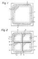
- Figure 1 is a plan view of the layout of each cell on a semiconductor chip of a conventional gate array LSI device
- Figs. 2 and 3 are plan views of the layout of each cell on a semiconductor chip of a gate array LSI device as an embodiment of the present invention
- Figs. 4A and 4B are electric circuit diagrams illustrating examples of basic cells used in the device shown in Figs. 2 and 3:
- Fig. 5A is a plan view of a structure of a basic cell unit used in the device shown in Fig. 3;
- Figs: 5B and 5C are sectional views taken on lines A-A and B-B of Fig. 5A, respectively;
- Fig. 6 is a circuit diagram of an electric circuit composed of a plurality of basic cell units as shown in Fig. 5A;
- Figs. 7A, 7B, and 7C are a partially sectional perspective view, plan view, and electric circuit diagram of a basic cell unit used in a gate array LSI device as another embodiment of the present invention.
- Figs. 8A and 8B are a plan view and electric circuit diagram of an example of connections of the basic cell unit shown in Fig. 7B;
- Fig. 9 is an electric circuit diagram of a circuit obtained by the connections shown in Figs. 8A and 8B.
- Fig. 1 illustrates the layout of each cell on a semiconductor chip of a conventional gate array LSI device.
- inner cells i.e., basic cells 2 are arranged, for example, in a matrix on a semiconductor chip 1, forming an inner cell array 3.
- Input/output cells 4 are arranged surrounding the inner cell array 3.
- circuits for realizing the desired function are formed by mutually combining the basic cells 2, and the input and output terminals of each of the circuits are connected to external circuits via the peripheral input/output cells 4.
- the conventional gate array LSI device is disadvantageous in that it has a low degree of freedom in circuit design, a low operating speed, and a high power consumption.
- Fig. 2 illustrates an arrangement of each cell on a semiconductor chip of a gate array LSI device as an embodiment of the present invention.
- four basic cell arrays 7-1, 7-2, 7-3, and 7-4 are formed, on a semiconductor chip 5, each comprising a first kind of basic cells 6 disposed, for example, in a matrix, a second kind of basic cells 8 disposed in the shape of a cross between the basic cell arrays 7-1, 7-2, 7-3, and 7-4, and input/ output cells 9 disposed in an outer circumference of an inner cell area wherein these basic cells are disposed.
- Each of the first kind of basic cells 6 comprises an output stage having a relatively small drive ability
- each of the second kind of basic cells 8 comprises an output stage having a relatively large drive ability.
- the first kind of basic cells 6 are used for forming a circuit with a relatively small output fan-out number or a circuit with an output terminal connected to relatively short length connection lines.
- the second kind of basic cells 8 are used for forming a circuit with a large fan-out number, and a circuit with relatively long output connections.
- the second kind of basic cells 8 are disposed in a cross-shape, thus dividing the first kind of basic cells 6 into four blocks, i.e., four basic cell arrays 7-1, 7-2, 7-3, and 7-4, it is possible to connect between the basic cell arrays via the second kind of basic cells 8. In this way, the long connection lines connecting the basic cell arrays are driven via the basic cells having a larger drive ability, and it is possible to avoid the decrease in the operating speed of the circuit and to realize a high speed circuit.
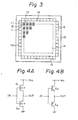
- Fig. 3 illustrates an arrangement of each cell on a semiconductor chip of a gate array LSI device as another embodiment of the present invention.
- a basic cell array 14 is formed by a matrix arrangement of basic cell units 13 on a semiconductor chip 10.
- Each of the basic cell units 13 is a combination of four first kind of basic cells 11, each having a small drive ability, and two second kind of basic cells 12 each having a large drive ability.
- the first kind of basic cells 11 are disposed surrounding the second kind of basic cells 12.
- the input/ output cells 15 are disposed along the outer circumference of the basic cell array 14.
- circuits with a large fan-out number and circuits with long output connection lines can be formed by using the second kind of basic cells 12.
- Other circuits can be formed by using the first kind of basic cells 11.
- the long connection lines in a semiconductor chip are driven by the basic cells 12 having a larger drive ability, making it possible to enlarge the operating speed of the circuits and to increase the degree of freedom in the circuit design.
- Figs. 4A and 4B illustrate the structures of the basic cells in the aforementioned embodiments.
- Fig. 4A illustrates a CMIS inverter circuit comprising a P-channel MIS transistor Q, and an n-channel MIS transistor Q 3 .
- Fig. 4B illustrates a bipolar type buffer circuit comprising an NPN transistor Q 3 and a PNP transistor Q 4 .
- the CMIS inverter of Fig. 4A or a CMIS type fundamental circuit having the output stage composed of the inverter circuit shown in Fig. 4A is used as a first kind of basic cell having a small drive ability
- the bipolar type buffer circuit shown in Fig. 4B can be used as a second kind of basic cell having a larger driver ability, or as the output stage of the second kind of basic cell.
- each of the aforementioned embodiments it is possible to arrange, for example, only a buffer circuit or driver having a large drive ability in the portion of each second kind of basic cell and to connect the output of each first kind of basic cell to another circuit via the driver.
- Figs. 5A, 5B, and 5C illustrate an example of a detailed structure of the basic cell unit 13 in the gate array LSI device of Fig. 3, in a plan view and sectional views taken on lines A-A and B-B thereof.
- the basic cell unit 13 comprises, for example, the first kind of basic cells 11 a and 11b, and the second kind of basic cells 12a and 12b formed on, for example, an n-type substrate 16 and on a p-type well 17 formed on the n-type substrate 16.
- Each of the first kind of basic cells 11 a comprises three p-type diffusion layers each being a drain or source and two gate electrodes, so that two p-channel MIS transistors are formed.
- Each of the first kind of basic cells 11 b comprises three n-type diffusion layers, each being a drain or source, and two gate electrodes which are common to those of the basic cell 11 b, so that two n-channel MIS transistors are formed.
- the second kind of basic cells 12a and 12b comprises a vertical npn-type bipolar transistor and a vertical pnp-type bipolar transistor, respectively. By using these transistors, it is possible to form, for example, the buffer circuit shown in Fig. 4B.
- FIG. 6 illustrates a circuit composed by using the basic cell units as shown in Figs. 5A, 5B and 5C.
- a basic cell unit 21 is used for forming a two-input MOS NAND gate and a bipolar buffer circuit.
- the two-input MOS NAND gate comprises two p-channel MOS transistors Q 5 and Q 6 formed by using the first kind of basic cell 11a, and two n-channel MOS transistors Q 7 and Q 8 formed by using the first kind of basic cell 11b.
- the bipolar buffer circuit comprises an npn-type transistor Q 9 and a pnp-type transistor Q 10 formed by using the second kind of basic cells 12a and 12b, respectively.
- Another basic cell unit 22 is used for forming a NOR gate comprising two p-channel MOS transistors Q 11 and Q 12 , and two n-channel MOS transistors Q 13 and Q 14 , by using the first kind of basic cells 11 a and 11 b.
- a basic cell unit 23 only the second kind of basic cells 12a and 12b are used to form a bipolar buffer comprising an npn-type transistor Q 15 and a pnp-type transistor Q 16 .
- a basic cell unit 24 is used for forming a MOS inverter comprising a p-channel MOS transistor Q 17 and an n-channel MOS transistor Q 18 , and a bipolar buffer comprising an npn-type transistor Q 19 and a pnp-type transistor Q 20'
- a basic cell unit 25 a NOR gate comprising two p-channel MOS transistors Q 21 and Q 22 and two n-channel MOS transistor Q 23 and Q 24 is formed by using the first kind of basic cells 11 a and 11 b.
- Figs. 7A, 7B, and 7C illustrate a basic cell unit used in a gate array LSI device as another embodiment of the present invention.
- Fig. 7B is a plan view and
- Fig. 7A is a partially sectional perspective view taken on line C-C of Fig. 7B.
- Fig. 7C illustrates an equivalent circuit of the basic cell unit.
- the basic cell unit shown in these drawings comprises the first kind of basic cells 31 a and 31b which have substantially the same structure as the first kind of basic cells 11a and 11 b and which are formed on an n-type semiconductor substrate 36 and on a p-type well 37, respectively.
- the basic cell unit further comprises the second kind of basic cells 32a and 32b.
- the second kind of basic cell 32a comprises a vertical npn-type transistor portion 34a, which is formed on an n-type substrate 36 and has substantially the same structure as the second kind of basic cell 12a shown in Fig. 5A.
- the second kind of basic cell 32a further comprises additional gate electrodes 33a formed between the transistor portion 34a and the adjacent first kind of basic cells 31a, and on the n-type substrate 36 via an insulation layer, e.g. Si0 2 (not shown).
- the second kind of basic cell 32b comprises a vertical pnp-type transistor portion 34b, which is formed on a p-type well 37 and has substantially the same structure as the second kind of basic cell 12b shown in Fig. 5A.
- the second kind of basic cell 32b further comprises additional gate electrodes 33b formed between the transistor portion 34b and the adjacent first kind of basic cells 31 b, and on the p-type substrate 37 via an insulation layer, e.g. Si0 2 (not shown).
- the number of the first kind of basic cells 31a a and 31 b and of the second kind of basic cells 32a and 32b included in one basic cell unit can be freely determined.
- the shaded areas designate n-type semiconductor . regions, and the small circles designate contact points or holes.
- the first kind of basic cells 31 a and 31 b comprises two p-type MIS transistors and two n-type MIS transistors, respectively.
- the second kind of basic cells 32a comprises an npn-type bipolar transistor and two p-channel MIS transistors each being composed of an additional gate 33a, p-type base region of the npn-type bipolar transistor, and adjacent p-type diffusion region of the basic cell 31a.
- the second kind of basic cells 32b comprises a pnp-type bipolar transistor and two n-channel MIS transistors.
- Each of the p-channel MIS transistors of the second kind of basic cell 32a and each of the n-channel MIS transistors of the second kind of basic cell 32b are used as control transistors for connecting or disconnecting between the basic cells 31 a and 32a and between the basic cells 31b and 32b.
- the ratio of MIS transistors and bipolar transistors included in one basic cell unit can be freely determined in accordance with the kind of circuits formed by using these transistors, performance requirements, and so on.
- the number of MIS transistors including those in the second kind of basic cells should be more than double the number of bipolar transistors, and the bipolar buffers should be used only when the fan-out number is larger than the predetermined number and/or the length of the output connection lines is longer than the predetermined length.
- Fig. 8A illustrates an example of connections of the basic cell unit shown in Fig. 7B
- Fig. 8B is an equivalent circuit of the device of Fig. 8A
- the first kind of basic cells 40a and 40b and the second kind of basic cells 41a and 41b are used to constitute a three-input NAND gate having an output bipolar buffer circuit.
- the second kind of basic cells 42a and 42b are used to constitute a bipolar buffer circuit.
- the thick solid lines show aluminum conductor lines.
- a control gate electrodes 43a of the second kind of basic cell 41 a and control gate electrodes 44a and 45a of the second kind of basic cell 42a are connected to a positive power supply voltage V+, so that a transistor Q 25 of the basic cell 41a a and transistors Q 26 and Q 27 of the basic cell 42a are all turned off.
- a control gate electrode 43b of the second kind of basic cell 41 b and control gate electrodes 44b and 45b of the second kind of basic cell 42b are connected to a negative power supply voltage V-, thereby turning off a transistor Q 28 of the second kind of basic cell 41 b and transistors Q 29 and Q 30 of the second kind of basic cell 42b. Therefore, each of the three-input NAND gates composed of the basic cells 40a, 41a, 40b, and 41b, and the bipolar buffer circuit composed of the basic cells 42a and 42b, is isolated from the other circuits.
- Fig. 9 is a clarified circuit diagram of the three-input NAND gate having the output bipolar buffer circuit shown in Fig. 8B and composed of the basic cells 40a, 41a, 40b, and 41b.
- three serially connected n-channel MOS transistors Q 31 , Q 32 , and Q 33 are in the basic cells 40b and 41b, and three parallely connected p-channel MOS transistors Q 34 , Q 33 , and Q 36 are in the basic cells 40a and 41a.
- the circuit of Fig. 9 operates as a NAND gate because the output signal OUT becomes low only when all the input signals IN 1 , IN 2 , and IN 3 are high. That is, when all the input signals IN 1 , IN 2 , and IN 3 are high, the n-channel"transistors Q 31 , Q 32 , and Q 33 are all turned on and the p-channel transistors Q 34 , Q 35 and Q 36 are all turned off, so that the output signal OUT becomes low. When at least one of the input signals IN 1 , IN 2 , and IN 3 is low, at least one of the p-channel transistors Q 34 , Q 35 , and Q 36 is turned on, thereby rendering the output signal OUT high.
- circuits having different drive ability can be used as basic cells, it is possible to greatly increase the degree of freedom in the circuit design of a gate array LSI device and to surely and reliably prevent the operating speed from being decreased by the lack of drive ability, thereby realizing a high performance LSI device.
- circuits having a larger drive ability are used only for portions necessitating a large drive ability, it is possible to avoid unnecessary power consumption and to increase the degree of integration of the circuits.
- the bipolar buffer portion can be used with the adjacent CMIS circuit portion or portions, or can be used independently, so that the degree of freedom of circuit design is further increased.
Landscapes
- Engineering & Computer Science (AREA)
- Power Engineering (AREA)
- Physics & Mathematics (AREA)
- Condensed Matter Physics & Semiconductors (AREA)
- General Physics & Mathematics (AREA)
- Computer Hardware Design (AREA)
- Microelectronics & Electronic Packaging (AREA)
- Manufacturing & Machinery (AREA)
- Design And Manufacture Of Integrated Circuits (AREA)
- Semiconductor Integrated Circuits (AREA)
- Metal-Oxide And Bipolar Metal-Oxide Semiconductor Integrated Circuits (AREA)
Claims (9)
Applications Claiming Priority (2)
| Application Number | Priority Date | Filing Date | Title |
|---|---|---|---|
| JP137698/83 | 1983-07-29 | ||
| JP58137698A JPS6035532A (ja) | 1983-07-29 | 1983-07-29 | マスタスライス集積回路装置 |
Publications (3)
| Publication Number | Publication Date |
|---|---|
| EP0133131A2 EP0133131A2 (fr) | 1985-02-13 |
| EP0133131A3 EP0133131A3 (en) | 1986-01-22 |
| EP0133131B1 true EP0133131B1 (fr) | 1989-01-04 |
Family
ID=15204716
Family Applications (1)
| Application Number | Title | Priority Date | Filing Date |
|---|---|---|---|
| EP84401568A Expired EP0133131B1 (fr) | 1983-07-29 | 1984-07-26 | Dispositif de circuit intégré du type "master slice" |
Country Status (5)
| Country | Link |
|---|---|
| US (1) | US4682202A (fr) |
| EP (1) | EP0133131B1 (fr) |
| JP (1) | JPS6035532A (fr) |
| KR (1) | KR890002966B1 (fr) |
| DE (1) | DE3475995D1 (fr) |
Families Citing this family (69)
| Publication number | Priority date | Publication date | Assignee | Title |
|---|---|---|---|---|
| JPS62119936A (ja) * | 1985-11-19 | 1987-06-01 | Fujitsu Ltd | コンプリメンタリ−lsiチツプ |
| JPS62189739A (ja) * | 1986-02-17 | 1987-08-19 | Hitachi Ltd | 半導体集積回路装置 |
| US4864381A (en) * | 1986-06-23 | 1989-09-05 | Harris Corporation | Hierarchical variable die size gate array architecture |
| JPH0650761B2 (ja) * | 1986-08-12 | 1994-06-29 | 富士通株式会社 | 半導体装置 |
| JPS6467940A (en) * | 1987-09-08 | 1989-03-14 | Mitsubishi Electric Corp | Semiconductor integrated circuit |
| US5185283A (en) * | 1987-10-22 | 1993-02-09 | Matsushita Electronics Corporation | Method of making master slice type integrated circuit device |
| JPH0831581B2 (ja) * | 1988-02-19 | 1996-03-27 | 株式会社東芝 | 半導体装置 |
| JPH01289138A (ja) * | 1988-05-16 | 1989-11-21 | Toshiba Corp | マスタースライス型半導体集積回路 |
| CA1309781C (fr) * | 1988-06-21 | 1992-11-03 | Colin Harris | Matrice de commutation analogique compacte a cmos |
| JPH0210869A (ja) * | 1988-06-29 | 1990-01-16 | Hitachi Ltd | 半導体装置 |
| US5019889A (en) * | 1988-06-29 | 1991-05-28 | Hitachi, Ltd. | Semiconductor integrated circuit device |
| NL194182C (nl) * | 1988-07-23 | 2001-08-03 | Samsung Electronics Co Ltd | Randloze moederschijf-halfgeleiderinrichting. |
| US5016080A (en) * | 1988-10-07 | 1991-05-14 | Exar Corporation | Programmable die size continuous array |
| DE69012848T2 (de) * | 1989-02-09 | 1995-03-09 | Sony Corp | Integrierte Halbleiterschaltungsanordnungen. |
| JP2632420B2 (ja) * | 1989-02-23 | 1997-07-23 | 三菱電機株式会社 | 半導体集積回路 |
| US5107147A (en) * | 1989-05-15 | 1992-04-21 | Texas Instruments Incorporated | Base cell for semi-custom circuit with merged technology |
| US4978633A (en) * | 1989-08-22 | 1990-12-18 | Harris Corporation | Hierarchical variable die size gate array architecture |
| FR2653952A1 (fr) * | 1989-10-31 | 1991-05-03 | Thomson Composants Microondes | Circuit integre logique prediffuse comportant au moins un amplificateur. |
| JPH03217055A (ja) * | 1990-01-22 | 1991-09-24 | Hitachi Ltd | 半導体集積回路装置 |
| US5015600A (en) * | 1990-01-25 | 1991-05-14 | Northern Telecom Limited | Method for making integrated circuits |
| DE4002780C2 (de) * | 1990-01-31 | 1995-01-19 | Fraunhofer Ges Forschung | Basiszelle für eine kanallose Gate-Array-Anordnung |
| US5289021A (en) * | 1990-05-15 | 1994-02-22 | Siarc | Basic cell architecture for mask programmable gate array with 3 or more size transistors |
| US5055716A (en) * | 1990-05-15 | 1991-10-08 | Siarc | Basic cell for bicmos gate array |
| JP2953755B2 (ja) * | 1990-07-16 | 1999-09-27 | 株式会社東芝 | マスタスライス方式の半導体装置 |
| JP2609746B2 (ja) * | 1990-07-19 | 1997-05-14 | 株式会社東芝 | 半導体装置 |
| JP2714996B2 (ja) * | 1990-08-08 | 1998-02-16 | 三菱電機株式会社 | 半導体集積回路装置 |
| JPH04103161A (ja) * | 1990-08-22 | 1992-04-06 | Toshiba Corp | バイポーラトランジスタ・絶縁ゲート型トランジスタ混載半導体装置 |
| JPH04200013A (ja) * | 1990-11-29 | 1992-07-21 | Hitachi Ltd | 論理回路 |
| US5313119A (en) * | 1991-03-18 | 1994-05-17 | Crosspoint Solutions, Inc. | Field programmable gate array |
| US5671397A (en) | 1993-12-27 | 1997-09-23 | At&T Global Information Solutions Company | Sea-of-cells array of transistors |
| US6675361B1 (en) * | 1993-12-27 | 2004-01-06 | Hyundai Electronics America | Method of constructing an integrated circuit comprising an embedded macro |
| US5391943A (en) * | 1994-01-10 | 1995-02-21 | Mahant-Shetti; Shivaling S. | Gate array cell with predefined connection patterns |
| US5440153A (en) * | 1994-04-01 | 1995-08-08 | United Technologies Corporation | Array architecture with enhanced routing for linear asics |
| US5629636A (en) * | 1994-10-19 | 1997-05-13 | Crosspoint Solutions, Inc. | Ram-logic tile for field programmable gate arrays |
| US5465055A (en) * | 1994-10-19 | 1995-11-07 | Crosspoint Solutions, Inc. | RAM-logic tile for field programmable gate arrays |
| JP3152145B2 (ja) * | 1996-02-28 | 2001-04-03 | 日本電気株式会社 | 半導体装置 |
| JP3768433B2 (ja) * | 2001-11-19 | 2006-04-19 | 株式会社ルネサステクノロジ | 半導体装置の設計方法 |
| JP2005268245A (ja) * | 2004-03-16 | 2005-09-29 | Nec Electronics Corp | 半導体装置の製造方法 |
| US7604947B2 (en) * | 2004-06-09 | 2009-10-20 | Cornell Research Foundation, Inc. | Detection and modulation of cancer stem cells |
| US7402846B2 (en) * | 2005-10-20 | 2008-07-22 | Atmel Corporation | Electrostatic discharge (ESD) protection structure and a circuit using the same |
| US8839175B2 (en) | 2006-03-09 | 2014-09-16 | Tela Innovations, Inc. | Scalable meta-data objects |
| US7943967B2 (en) * | 2006-03-09 | 2011-05-17 | Tela Innovations, Inc. | Semiconductor device and associated layouts including diffusion contact placement restriction based on relation to linear conductive segments |
| US8245180B2 (en) | 2006-03-09 | 2012-08-14 | Tela Innovations, Inc. | Methods for defining and using co-optimized nanopatterns for integrated circuit design and apparatus implementing same |
| US7446352B2 (en) * | 2006-03-09 | 2008-11-04 | Tela Innovations, Inc. | Dynamic array architecture |
| US8448102B2 (en) | 2006-03-09 | 2013-05-21 | Tela Innovations, Inc. | Optimizing layout of irregular structures in regular layout context |
| US9563733B2 (en) | 2009-05-06 | 2017-02-07 | Tela Innovations, Inc. | Cell circuit and layout with linear finfet structures |
| US7763534B2 (en) | 2007-10-26 | 2010-07-27 | Tela Innovations, Inc. | Methods, structures and designs for self-aligning local interconnects used in integrated circuits |
| US8658542B2 (en) | 2006-03-09 | 2014-02-25 | Tela Innovations, Inc. | Coarse grid design methods and structures |
| US8225239B2 (en) | 2006-03-09 | 2012-07-17 | Tela Innovations, Inc. | Methods for defining and utilizing sub-resolution features in linear topology |
| US8247846B2 (en) | 2006-03-09 | 2012-08-21 | Tela Innovations, Inc. | Oversized contacts and vias in semiconductor chip defined by linearly constrained topology |
| US8653857B2 (en) | 2006-03-09 | 2014-02-18 | Tela Innovations, Inc. | Circuitry and layouts for XOR and XNOR logic |
| US9230910B2 (en) | 2006-03-09 | 2016-01-05 | Tela Innovations, Inc. | Oversized contacts and vias in layout defined by linearly constrained topology |
| US8225261B2 (en) | 2006-03-09 | 2012-07-17 | Tela Innovations, Inc. | Methods for defining contact grid in dynamic array architecture |
| US7908578B2 (en) * | 2007-08-02 | 2011-03-15 | Tela Innovations, Inc. | Methods for designing semiconductor device with dynamic array section |
| US9035359B2 (en) | 2006-03-09 | 2015-05-19 | Tela Innovations, Inc. | Semiconductor chip including region including linear-shaped conductive structures forming gate electrodes and having electrical connection areas arranged relative to inner region between transistors of different types and associated methods |
| US8541879B2 (en) | 2007-12-13 | 2013-09-24 | Tela Innovations, Inc. | Super-self-aligned contacts and method for making the same |
| US9009641B2 (en) | 2006-03-09 | 2015-04-14 | Tela Innovations, Inc. | Circuits with linear finfet structures |
| US7932545B2 (en) * | 2006-03-09 | 2011-04-26 | Tela Innovations, Inc. | Semiconductor device and associated layouts including gate electrode level region having arrangement of six linear conductive segments with side-to-side spacing less than 360 nanometers |
| US7956421B2 (en) | 2008-03-13 | 2011-06-07 | Tela Innovations, Inc. | Cross-coupled transistor layouts in restricted gate level layout architecture |
| DK1945821T3 (da) | 2006-06-06 | 2011-03-07 | Gen Probe Inc | Mærkede oligonukleotider og anvendelse deraf i fremgangsmåder til amplifikation af nukleinsyrer |
| US7979829B2 (en) | 2007-02-20 | 2011-07-12 | Tela Innovations, Inc. | Integrated circuit cell library with cell-level process compensation technique (PCT) application and associated methods |
| US8286107B2 (en) | 2007-02-20 | 2012-10-09 | Tela Innovations, Inc. | Methods and systems for process compensation technique acceleration |
| US8667443B2 (en) | 2007-03-05 | 2014-03-04 | Tela Innovations, Inc. | Integrated circuit cell library for multiple patterning |
| US8453094B2 (en) | 2008-01-31 | 2013-05-28 | Tela Innovations, Inc. | Enforcement of semiconductor structure regularity for localized transistors and interconnect |
| US7939443B2 (en) | 2008-03-27 | 2011-05-10 | Tela Innovations, Inc. | Methods for multi-wire routing and apparatus implementing same |
| MY152456A (en) | 2008-07-16 | 2014-09-30 | Tela Innovations Inc | Methods for cell phasing and placement in dynamic array architecture and implementation of the same |
| US9122832B2 (en) | 2008-08-01 | 2015-09-01 | Tela Innovations, Inc. | Methods for controlling microloading variation in semiconductor wafer layout and fabrication |
| US8661392B2 (en) | 2009-10-13 | 2014-02-25 | Tela Innovations, Inc. | Methods for cell boundary encroachment and layouts implementing the Same |
| US9159627B2 (en) | 2010-11-12 | 2015-10-13 | Tela Innovations, Inc. | Methods for linewidth modification and apparatus implementing the same |
Family Cites Families (10)
| Publication number | Priority date | Publication date | Assignee | Title |
|---|---|---|---|---|
| US3609479A (en) * | 1968-02-29 | 1971-09-28 | Westinghouse Electric Corp | Semiconductor integrated circuit having mis and bipolar transistor elements |
| JPS5925381B2 (ja) * | 1977-12-30 | 1984-06-16 | 富士通株式会社 | 半導体集積回路装置 |
| JPS57181152A (en) * | 1981-04-30 | 1982-11-08 | Toshiba Corp | Semiconductor integrated circuit device |
| JPS5856354A (ja) * | 1981-09-30 | 1983-04-04 | Hitachi Ltd | マスタ−スライスlsi |
| JPS5871650A (ja) * | 1981-10-26 | 1983-04-28 | Hitachi Ltd | 半導体集積回路装置 |
| JPS5885558A (ja) * | 1981-11-17 | 1983-05-21 | Olympus Optical Co Ltd | セミカスタム半導体装置 |
| JPS5890758A (ja) * | 1981-11-25 | 1983-05-30 | Mitsubishi Electric Corp | 相補形集積回路装置 |
| GB2122417B (en) * | 1982-06-01 | 1985-10-09 | Standard Telephones Cables Ltd | Integrated circuits |
| JPS59177944A (ja) * | 1983-03-28 | 1984-10-08 | Hitachi Ltd | 半導体集積回路装置 |
| JPH0669142B2 (ja) * | 1983-04-15 | 1994-08-31 | 株式会社日立製作所 | 半導体集積回路装置 |
-
1983
- 1983-07-29 JP JP58137698A patent/JPS6035532A/ja active Pending
-
1984
- 1984-07-26 DE DE8484401568T patent/DE3475995D1/de not_active Expired
- 1984-07-26 EP EP84401568A patent/EP0133131B1/fr not_active Expired
- 1984-07-28 KR KR1019840004506A patent/KR890002966B1/ko not_active IP Right Cessation
- 1984-07-30 US US06/635,680 patent/US4682202A/en not_active Expired - Fee Related
Also Published As
| Publication number | Publication date |
|---|---|
| KR890002966B1 (ko) | 1989-08-14 |
| US4682202A (en) | 1987-07-21 |
| EP0133131A2 (fr) | 1985-02-13 |
| KR850000800A (ko) | 1985-03-09 |
| DE3475995D1 (en) | 1989-02-09 |
| JPS6035532A (ja) | 1985-02-23 |
| EP0133131A3 (en) | 1986-01-22 |
Similar Documents
| Publication | Publication Date | Title |
|---|---|---|
| EP0133131B1 (fr) | Dispositif de circuit intégré du type "master slice" | |
| US4733288A (en) | Gate-array chip | |
| US6166560A (en) | Basic cell structure having a plurality of transistors for master slice type semiconductor integrated circuit device | |
| US4651190A (en) | Semiconductor integrated circuit | |
| US5663662A (en) | Library group and semiconductor integrated circuit structured thereof | |
| US5493135A (en) | Symmetrical multi-layer metal logic array with continuous substrate taps and extension portions for increased gate density | |
| KR100511808B1 (ko) | 반도체 집적회로장치 및 그 제조방법 | |
| EP0177336B1 (fr) | Structure intégrée de matrice de portes | |
| US4783692A (en) | CMOS gate array | |
| US5378941A (en) | Bipolar transistor MOS transistor hybrid semiconductor integrated circuit device | |
| US5552618A (en) | Multi-voltage-lever master-slice integrated circuit | |
| US5539246A (en) | Microelectronic integrated circuit including hexagonal semiconductor "gate " device | |
| US8178904B2 (en) | Gate array | |
| JP3520659B2 (ja) | 複数の電源電圧で駆動されるゲートアレイ及びそれを用いた電子機器 | |
| US5001487A (en) | Semiconductor integrated circuit device | |
| JPH0127578B2 (fr) | ||
| US5391943A (en) | Gate array cell with predefined connection patterns | |
| US5654563A (en) | Microelectronic integrated circuit including triangular semiconductor "or"g | |
| US5631581A (en) | Microelectronic integrated circuit including triangular semiconductor "and" gate device | |
| US4851891A (en) | Gate array having transistor buried in interconnection region | |
| US4716450A (en) | Semiconductor integrated circuit having complementary field effect transistors | |
| JP3019764B2 (ja) | 半導体集積回路装置およびその回路セルの多段接続構造 | |
| US20240079411A1 (en) | Layout structure, semiconductor structure and memory | |
| EP0495990A1 (fr) | Dispositif semi-conducteur | |
| JPH0653450A (ja) | マスタースライス方式の半導体集積回路装置 |
Legal Events
| Date | Code | Title | Description |
|---|---|---|---|
| PUAI | Public reference made under article 153(3) epc to a published international application that has entered the european phase |
Free format text: ORIGINAL CODE: 0009012 |
|
| AK | Designated contracting states |
Designated state(s): DE FR GB |
|
| PUAL | Search report despatched |
Free format text: ORIGINAL CODE: 0009013 |
|
| AK | Designated contracting states |
Designated state(s): DE FR GB |
|
| 17P | Request for examination filed |
Effective date: 19860609 |
|
| 17Q | First examination report despatched |
Effective date: 19880407 |
|
| GRAA | (expected) grant |
Free format text: ORIGINAL CODE: 0009210 |
|
| AK | Designated contracting states |
Kind code of ref document: B1 Designated state(s): DE FR GB |
|
| REF | Corresponds to: |
Ref document number: 3475995 Country of ref document: DE Date of ref document: 19890209 |
|
| ET | Fr: translation filed | ||
| PLBE | No opposition filed within time limit |
Free format text: ORIGINAL CODE: 0009261 |
|
| STAA | Information on the status of an ep patent application or granted ep patent |
Free format text: STATUS: NO OPPOSITION FILED WITHIN TIME LIMIT |
|
| 26N | No opposition filed | ||
| PGFP | Annual fee paid to national office [announced via postgrant information from national office to epo] |
Ref country code: GB Payment date: 19920428 Year of fee payment: 9 |
|
| PGFP | Annual fee paid to national office [announced via postgrant information from national office to epo] |
Ref country code: FR Payment date: 19920730 Year of fee payment: 9 |
|
| PGFP | Annual fee paid to national office [announced via postgrant information from national office to epo] |
Ref country code: DE Payment date: 19920922 Year of fee payment: 9 |
|
| PG25 | Lapsed in a contracting state [announced via postgrant information from national office to epo] |
Ref country code: GB Effective date: 19930726 |
|
| GBPC | Gb: european patent ceased through non-payment of renewal fee |
Effective date: 19930726 |
|
| PG25 | Lapsed in a contracting state [announced via postgrant information from national office to epo] |
Ref country code: FR Effective date: 19940331 |
|
| PG25 | Lapsed in a contracting state [announced via postgrant information from national office to epo] |
Ref country code: DE Effective date: 19940401 |
|
| REG | Reference to a national code |
Ref country code: FR Ref legal event code: ST |